Power Sharing and Voltage Vector Distribution Model of a Dual Inverter Open-End Winding Motor Drive System for Electric Vehicles


Abstract
:Featured Application
Abstract
1. Introduction
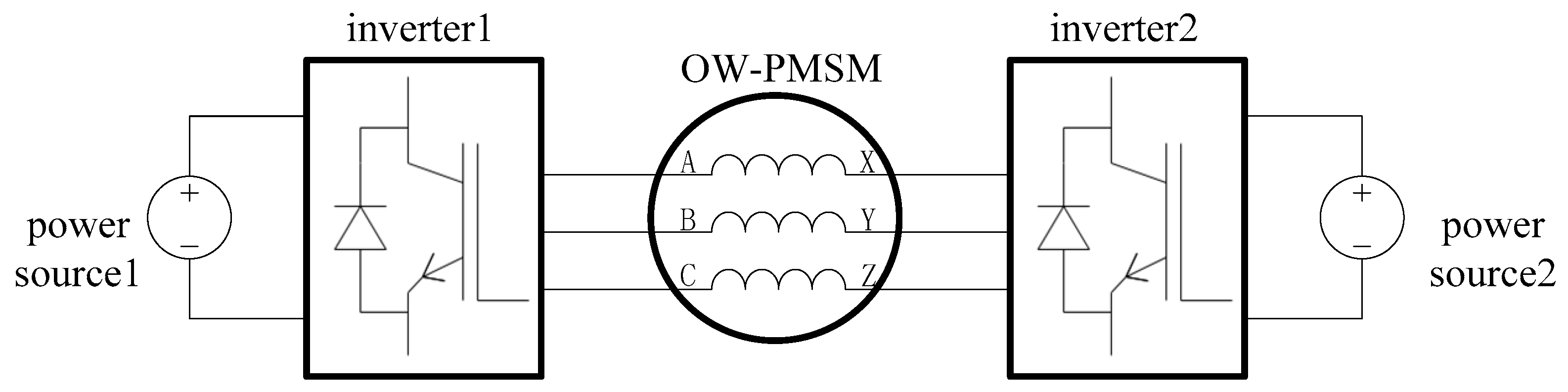
2. Operating Principle
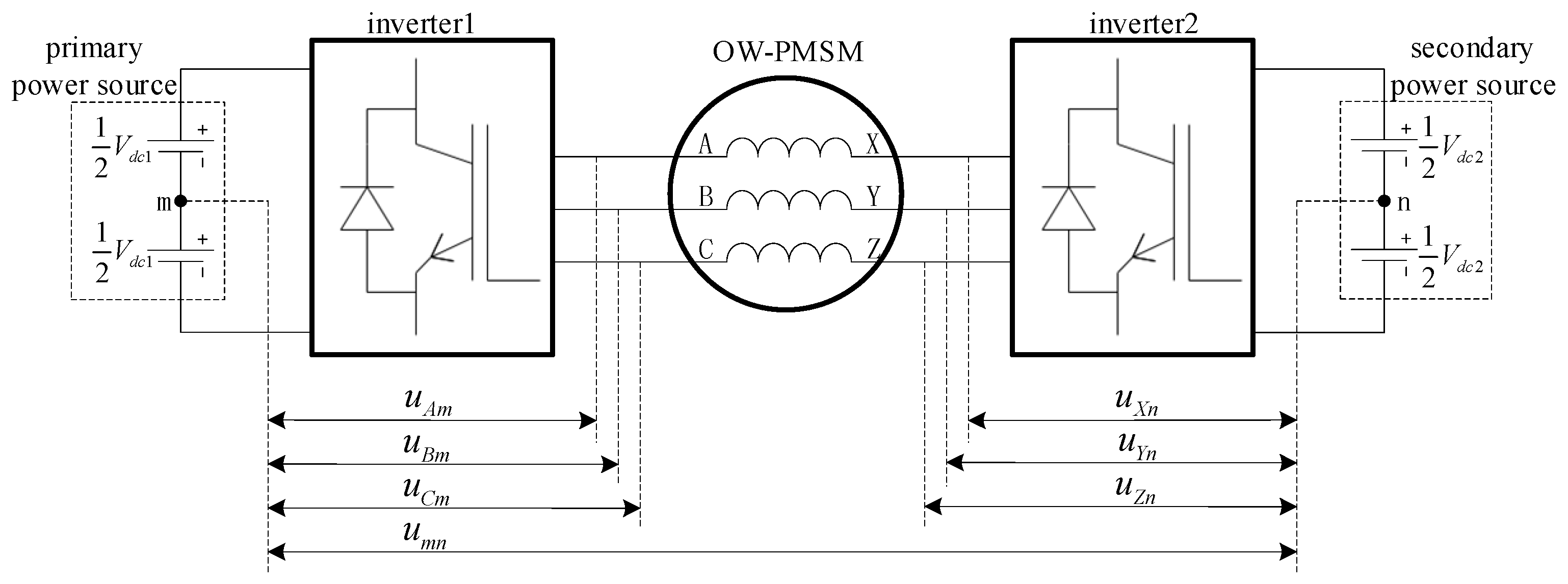
2.1. System Modeling
2.2. Principle of Power Flow
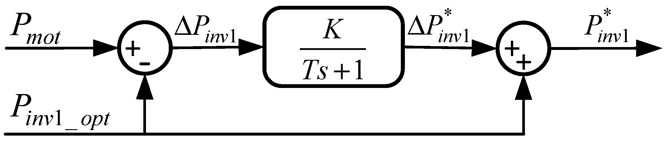
3. Desired Power Sharing Calculation Method
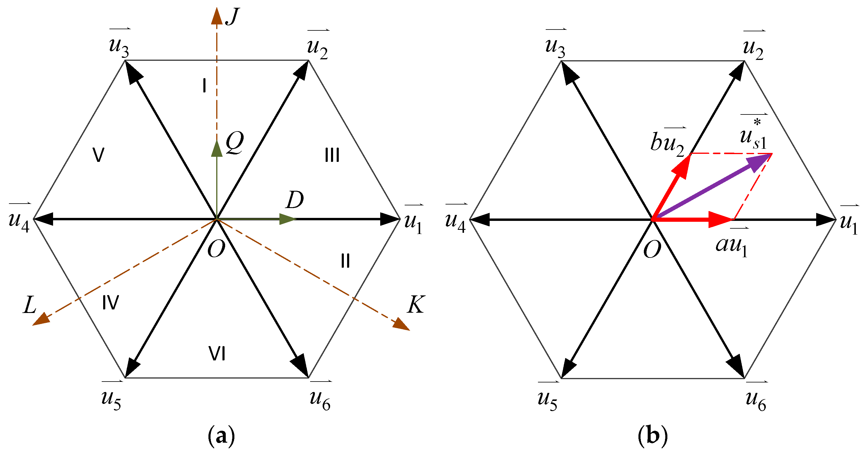
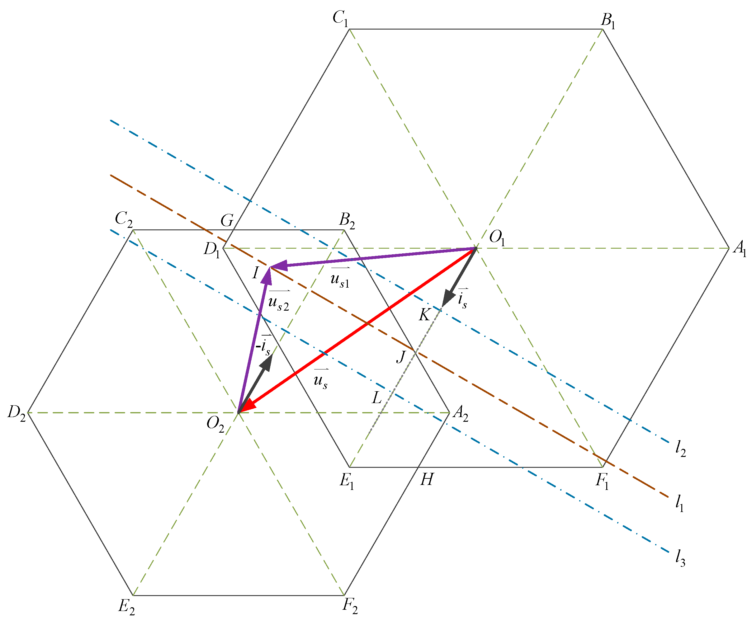
4. Voltage Vector Distribution Method
4.1. Voltage Vector Over Range Judgmental Algorithm
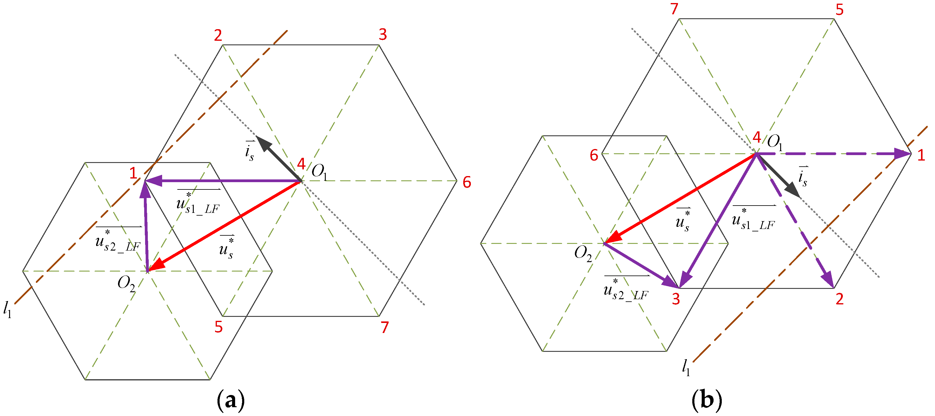
4.2. Low Switching Frequency Method
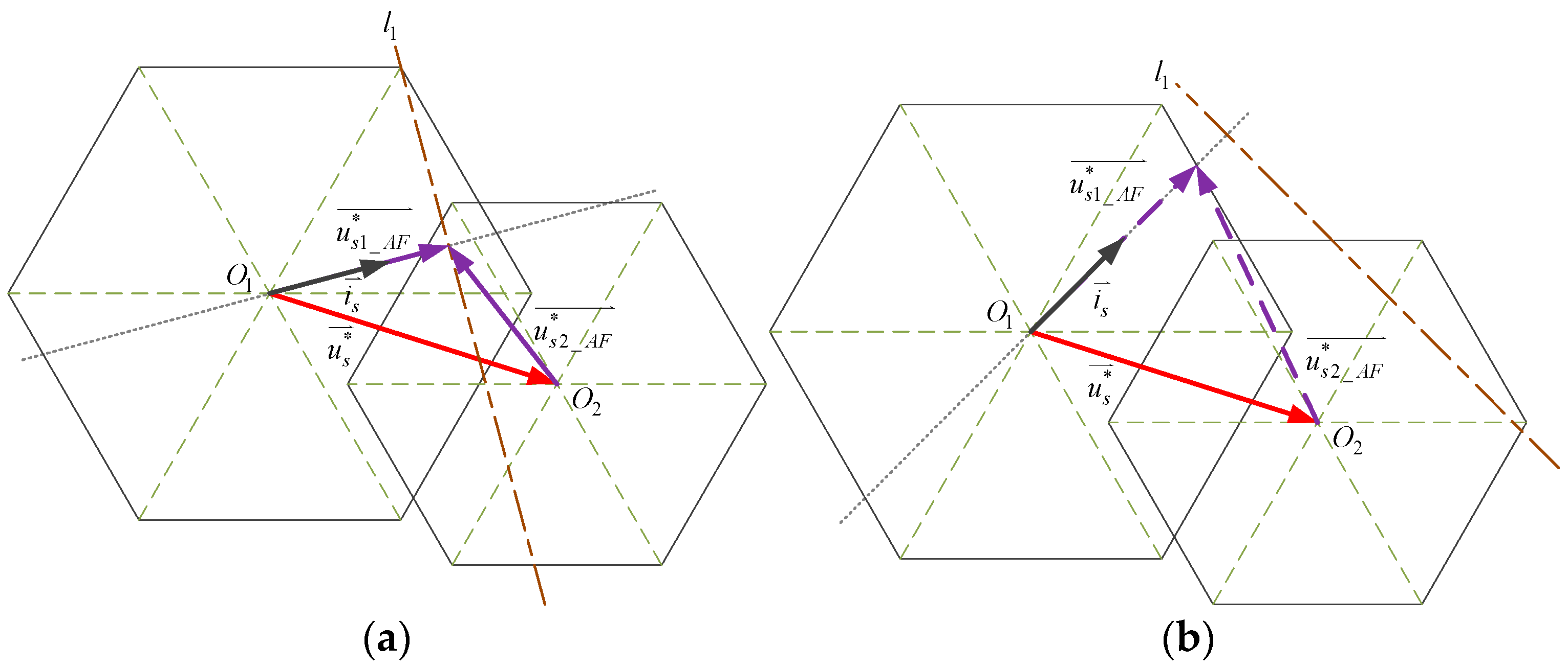
4.3. Accurate Power Following Method
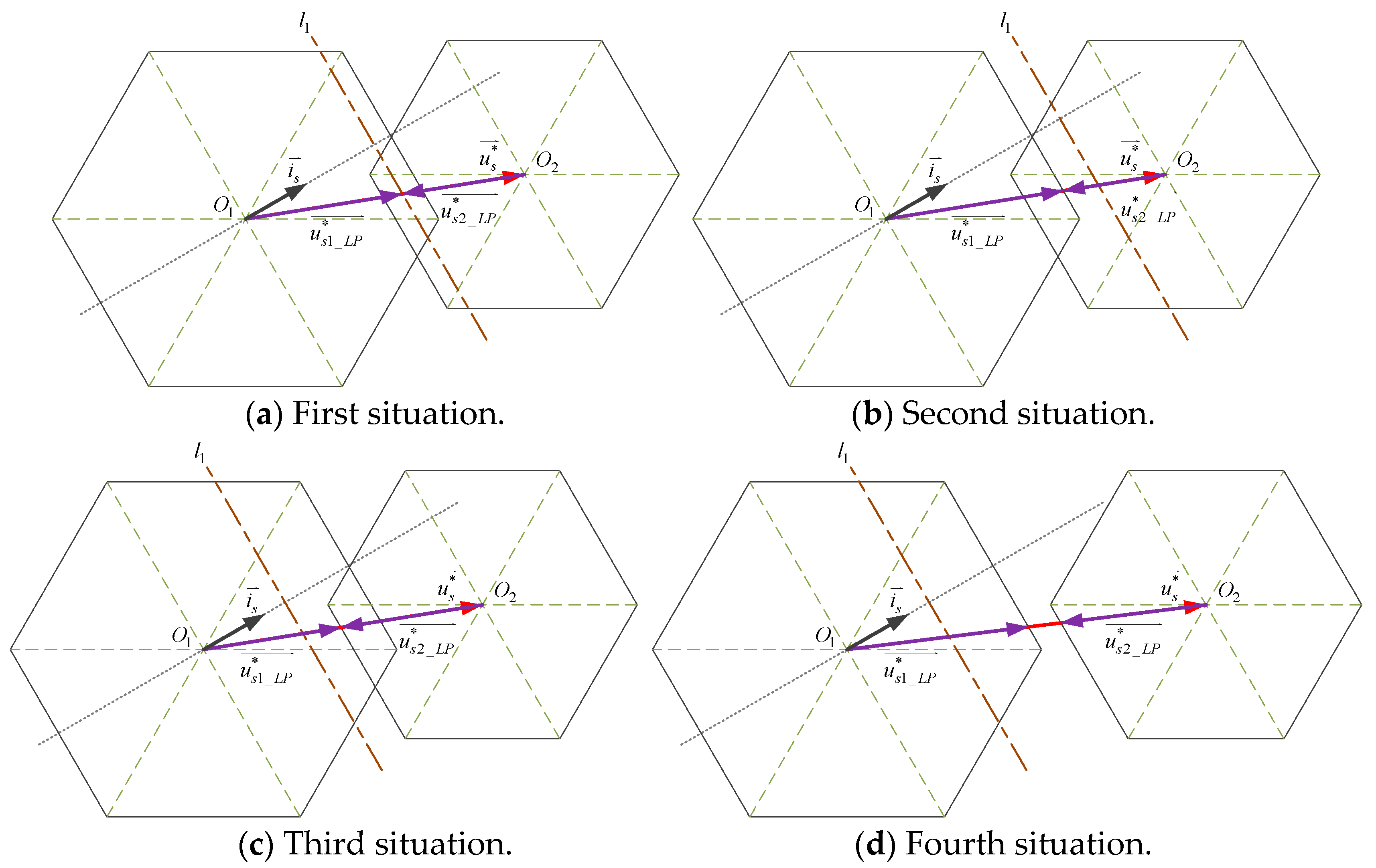
4.4. Linear Partition Method
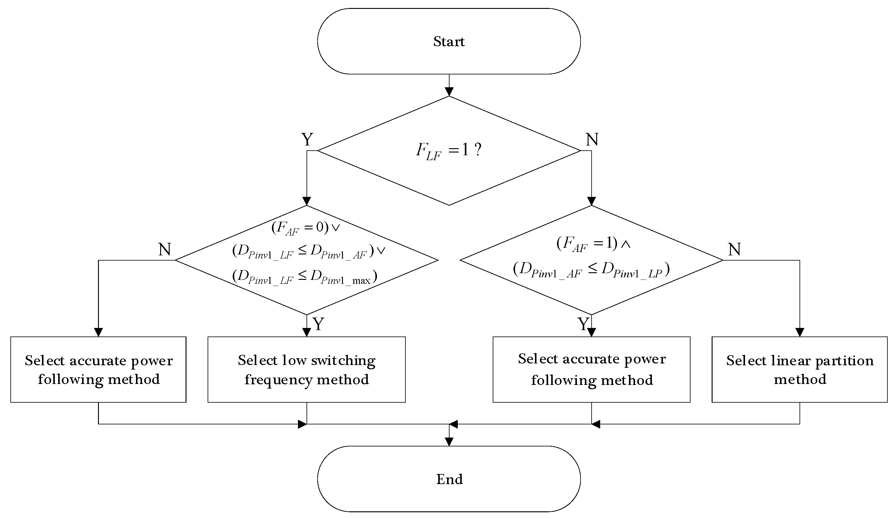
4.5. Voltage Vector Distribution Method Selection Strategy
5. Drive System Simulation
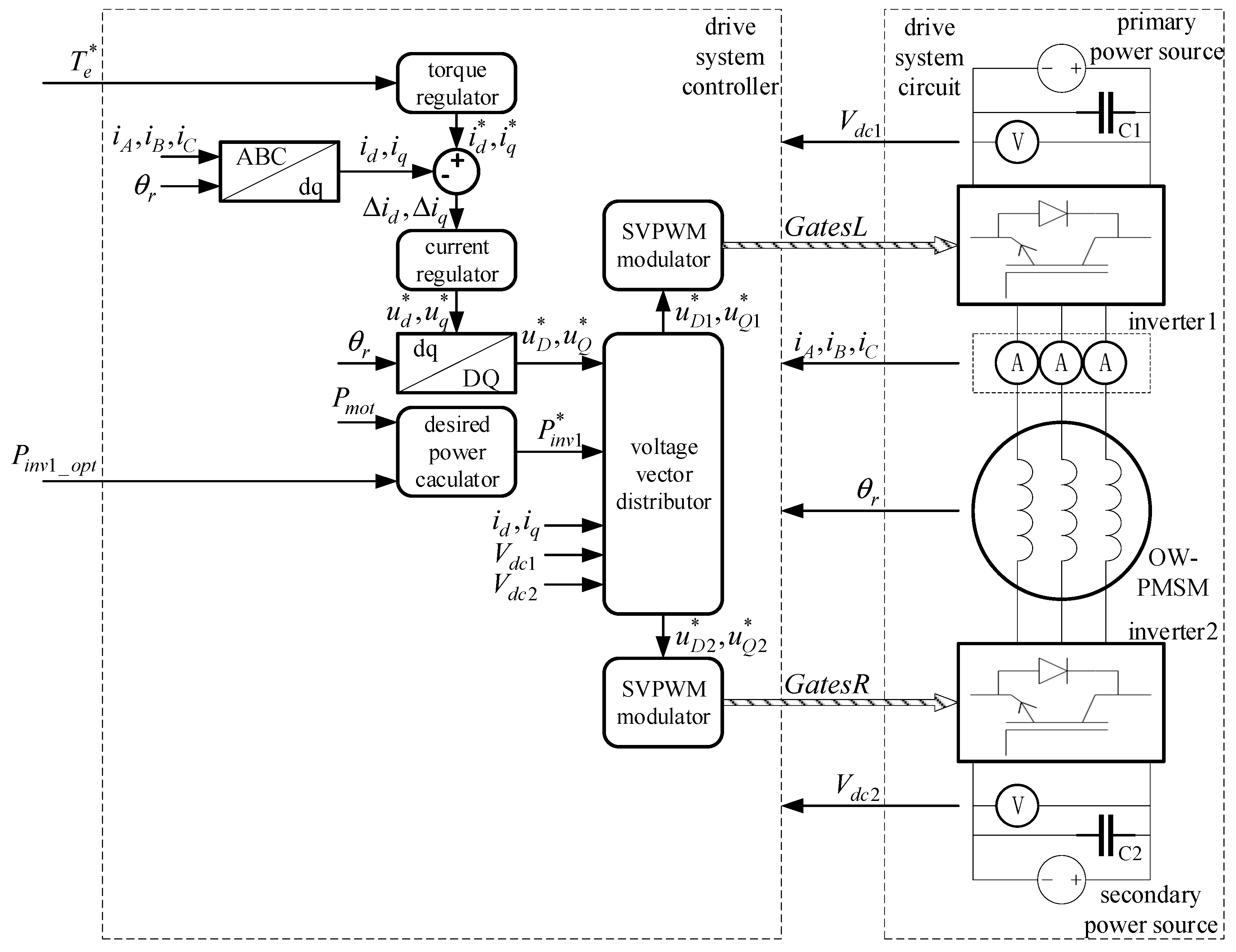
5.1. Overall Configuration
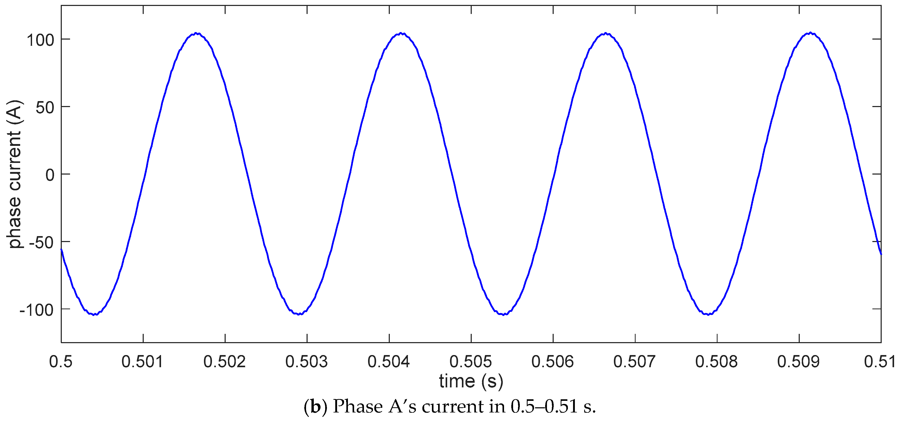
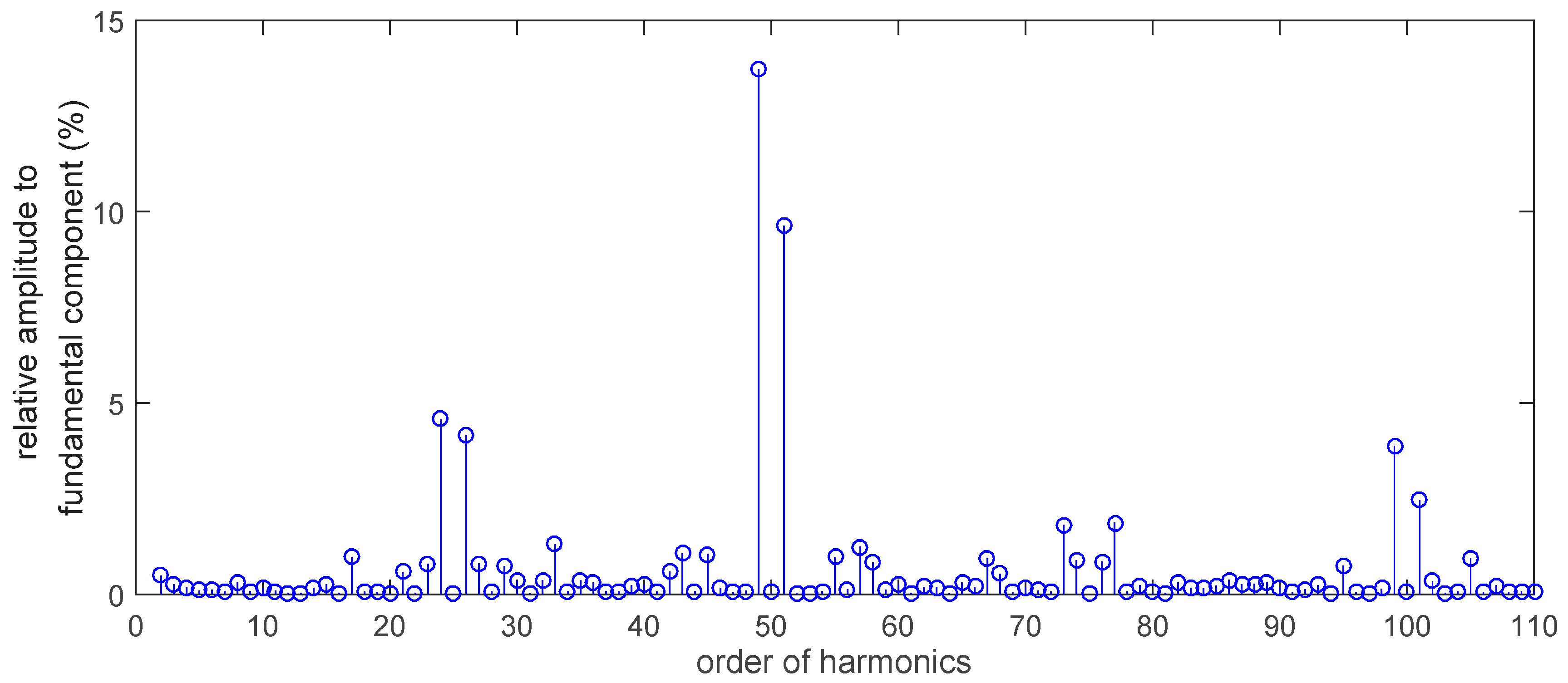
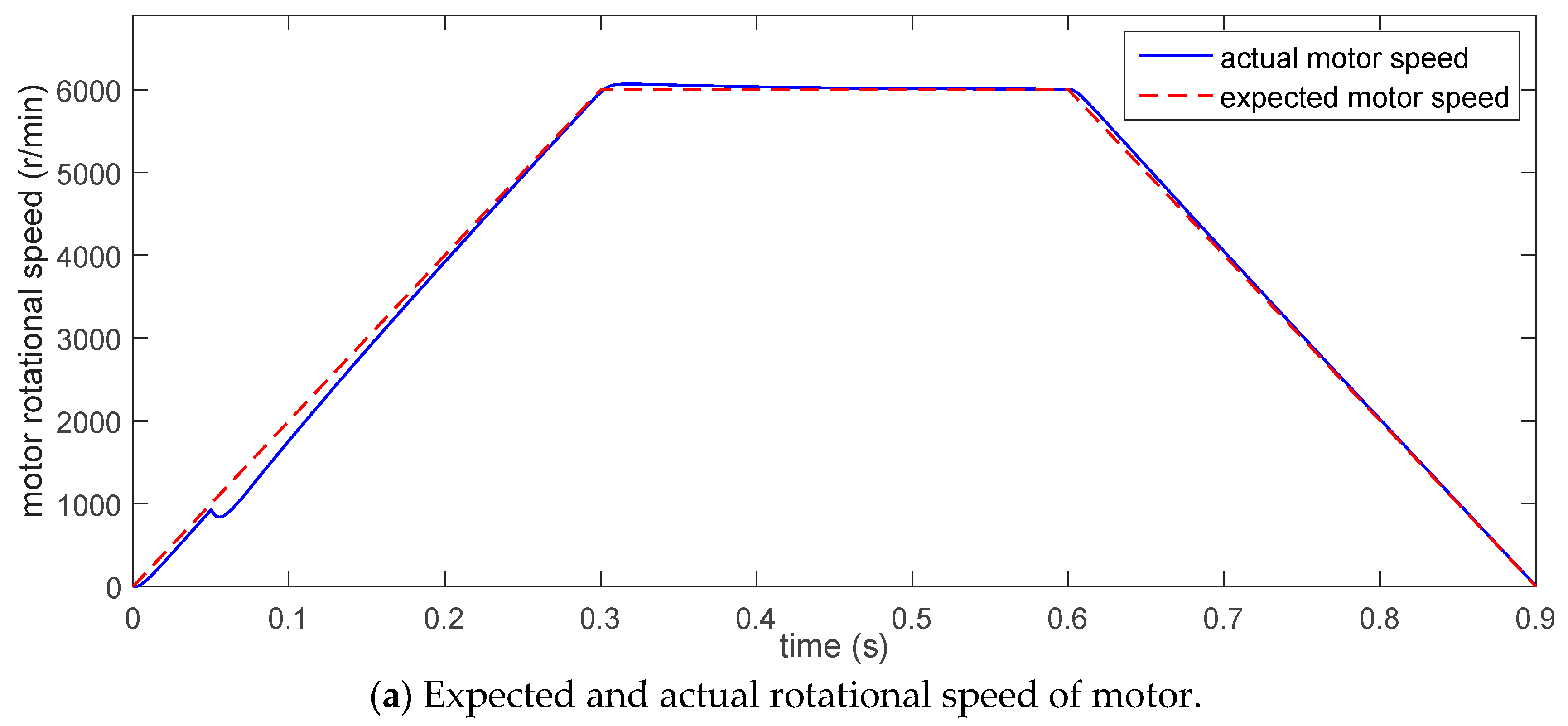
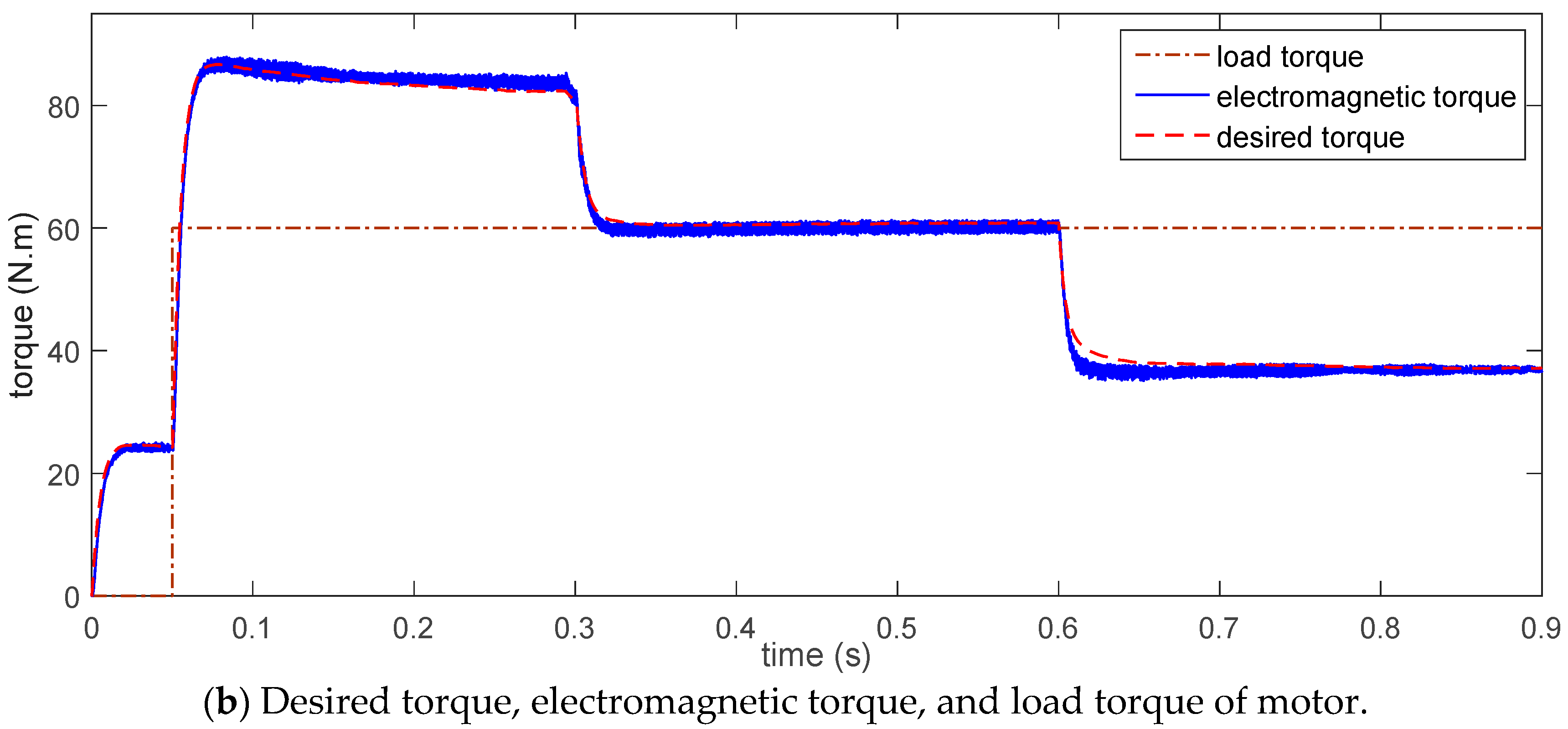
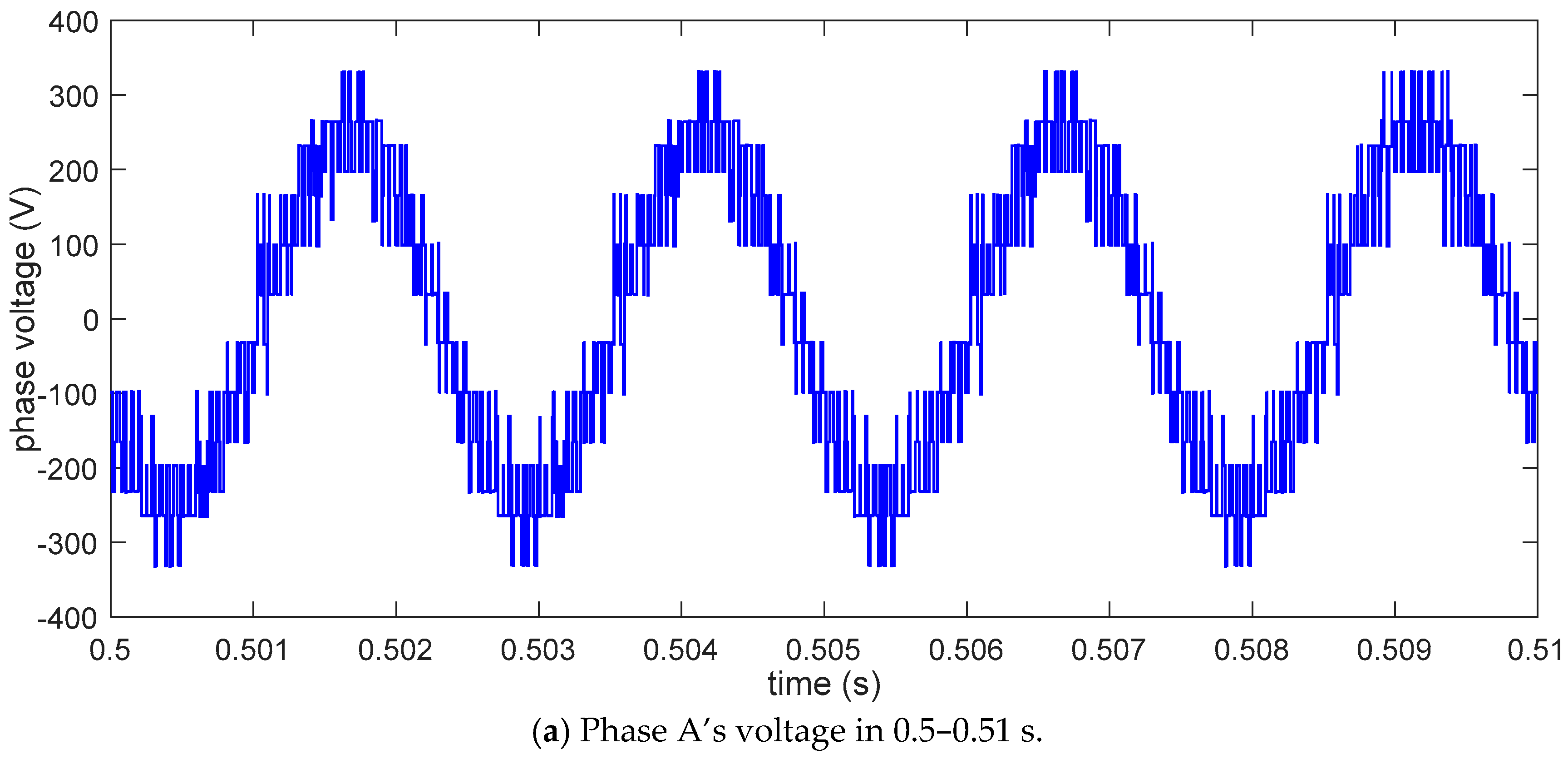
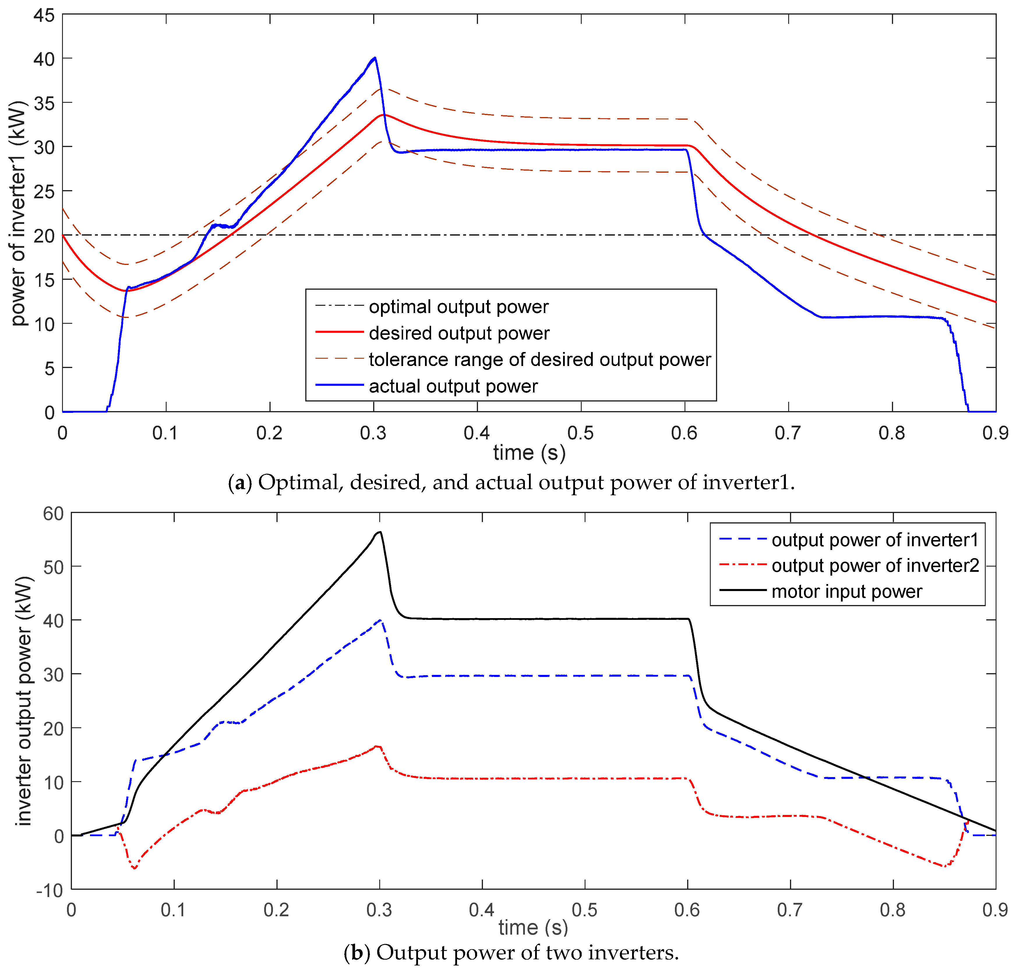
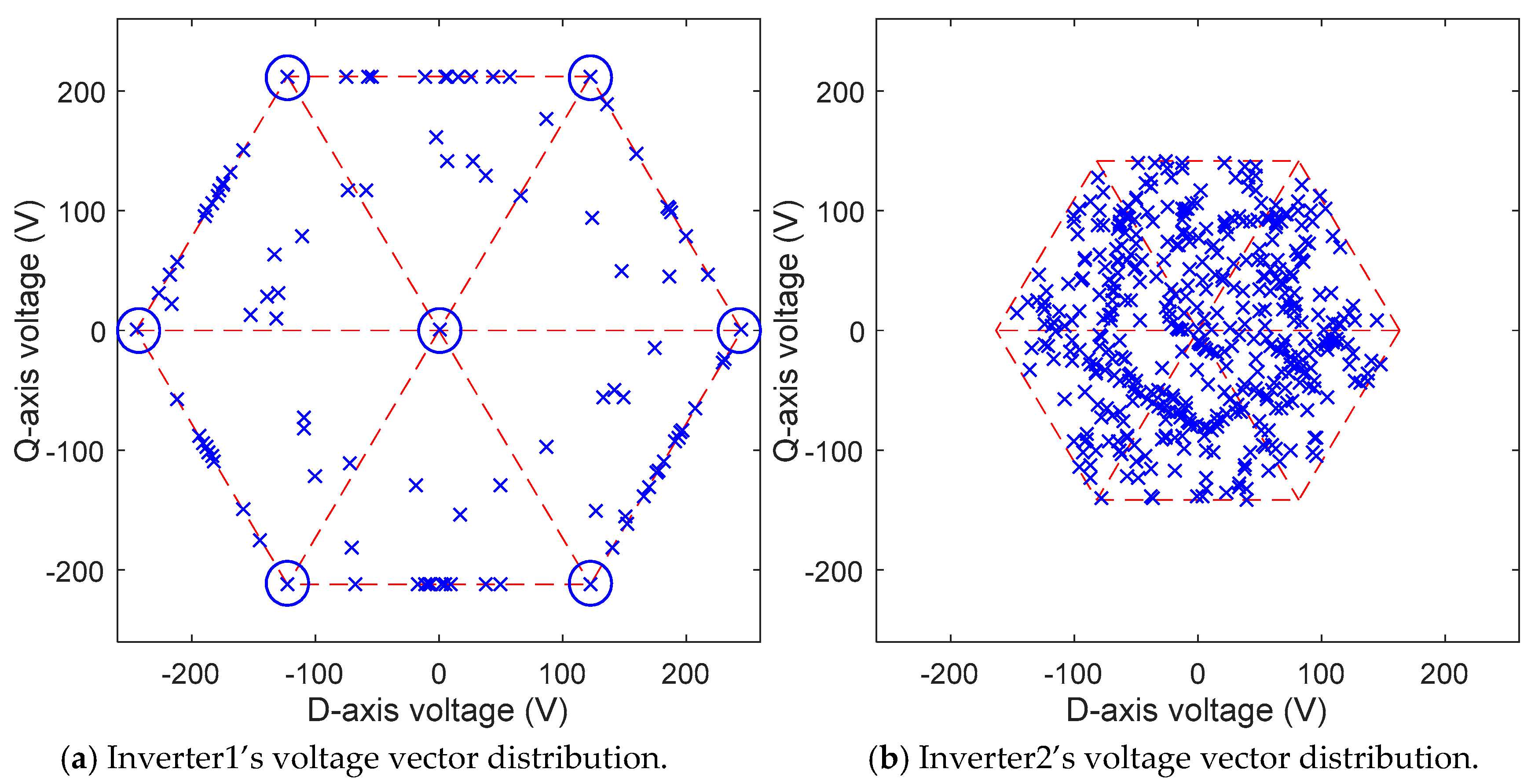
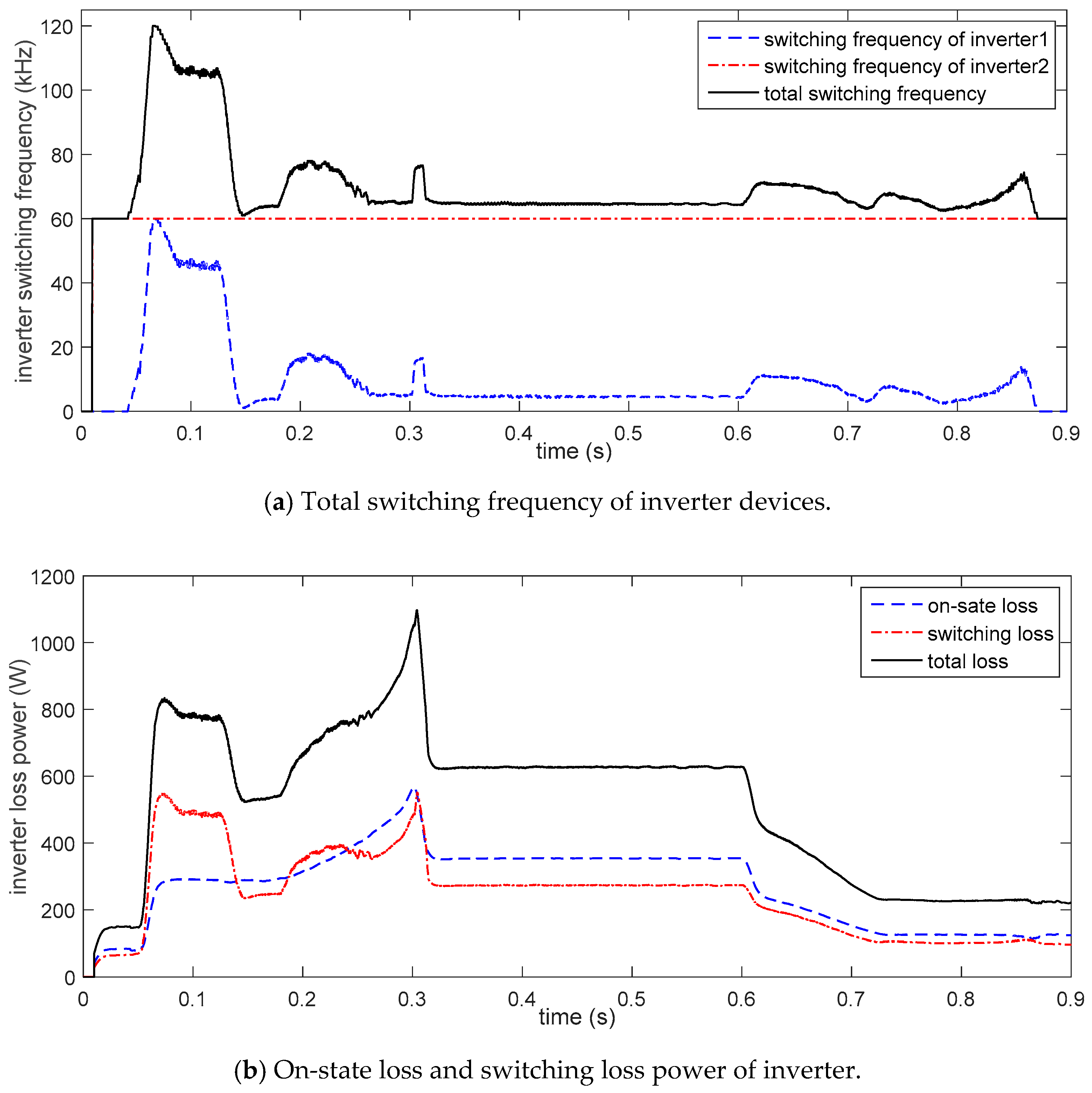
5.2. Simulation Results
6. Conclusions
Acknowledgments
Author Contributions
Conflicts of Interest
References
- Park, J.W.; Koo, D.H.; Kim, J.M.; Kim, H.G. Improvement of control characteristics of interior permanent magnet synchronous motor for electric vehicle. IEEE Trans. Ind. Appl. 2001, 37, 1754–1760. [Google Scholar] [CrossRef]
- Boazzo, B.; Pellegrino, G. Model-based direct flux vector control of permanent-magnet synchronous motor drives. IEEE Trans. Ind. Appl. 2015, 51, 3126–3136. [Google Scholar] [CrossRef]
- Park, C.S.; Lee, J.S. A torque error compensation algorithm for surface mounted permanent magnet synchronous machines with respect to magnet temperature variations. Energies 2017, 10, 1365. [Google Scholar] [CrossRef]
- Nam, K.-T.; Kim, H.; Lee, S.-J.; Kuc, T.-Y. Observer-Based Rejection of Cogging Torque Disturbance for Permanent Magnet Motors. Appl. Sci. 2017, 7, 867. [Google Scholar] [CrossRef]
- Wu, H.X.; Li, L.Y.; Kou, B.Q.; Ping, Z. The research on energy regeneration of permanent magnet synchronous motor used for hybrid electric vehicle. In Proceedings of the Vehicle Power and Propulsion Conference (VPPC ’08), Harbin, China, 3–5 September 2008; pp. 1–4. [Google Scholar] [CrossRef]
- Howlader, A.M.; Urasaki, N.; Senjyu, T.; Yona, A.; Saber, A.Y. Optimal pam control for a buck boost dc-dc converter with a wide-speed-range of operation for a PMSM. J. Power Electron. 2010, 10, 477–484. [Google Scholar] [CrossRef]
- Athavale, A.; Sasaki, K.; Gagas, B.S.; Kato, T.; Lorenz, R. Variable flux permanent magnet synchronous machine (VF-PMSM) design methodologies to meet electric vehicle traction requirements with reduced losses. IEEE Trans. Ind. Appl. 2017, 1–8. [Google Scholar] [CrossRef]
- Howlader, A.M.; Urasaki, N.; Senjyu, T.; Yona, A. Wide-Speed-Range optimal PAM control for permanent magnet synchronous motor. In Proceedings of the IEEE International Conference on Electrical Machines and Systems, Tokyo, Japan, 15–18 November 2009; Volume 2007, pp. 1–5. [Google Scholar]
- Li, Z.; Onar, O.; Khaligh, A.; Schaltz, E. Design and control of a multiple input DC/DC converter for battery/ultra-capacitor based electric vehicle power system. In Proceedings of the IEEE Applied Power Electronics Conference and Exposition, Washington, DC, USA, 15–19 February 2009; pp. 591–596. [Google Scholar]
- Gualous, H.; Gustin, F.; Berthon, A.; Dakyo, B. DC/DC converter design for supercapacitor and battery power management in hybrid vehicle applications—Polynomial control strategy. IRE Trans. Ind. Electron. 2010, 57, 587–597. [Google Scholar] [CrossRef]
- An, Q.; Liu, J.; Peng, Z.; Sun, L.; Sun, L. Dual-space vector control of open-end winding permanent magnet synchronous motor drive fed by dual inverter. IEEE Trans. Power Electron. 2016, 31, 8329–8342. [Google Scholar] [CrossRef]
- Nguyen, N.K.; Semail, E.; Meinguet, F.; Sandulescu, P.; Kestelyn, X.; Aslan, B. Different virtual stator winding configurations of open-end winding five-phase PM machines for wide speed range without flux weakening operation. In Proceedings of the IEEE European Conference on Power Electronics and Applications, Lille, France, 2–6 September 2013; pp. 1–8. [Google Scholar]
- Sandulescu, P.; Meinguet, F.; Kestelyn, X.; Semail, E.; Bruyere, A. Control strategies for open-end winding drives operating in the flux-weakening region. IEEE Trans. Power Electron. 2014, 29, 4829–4842. [Google Scholar] [CrossRef]
- Kwak, M.S.; Sul, S.K. Flux weakening control of an open winding machine with isolated dual inverters. In Proceedings of the IEEE Industry Applications Conference 2007, New Orleans, LA, USA, 23–27 September 2007; pp. 251–255. [Google Scholar]
- Welchko, B.A. A double-ended inverter system for the combined propulsion and energy management functions in hybrid vehicles with energy storage. In Proceedings of the IEEE Industrial Electronics Society, Raleigh, NC, USA, 6–10 November 2005; p. 6. [Google Scholar]
- Machiya, H.; Haga, H.; Kondo, S. High efficiency drive method of an open-winding induction machine driven by dual inverter using capacitor across dc bus. Electr. Eng. Jpn. 2016, 197, 62–72. [Google Scholar] [CrossRef]
- Drisya, V.; Samina, T. Supply voltage boosting using a floating capacitor bridge in a 3 level space vector modulated inverter system for an open-end winding induction motor drive. In Proceedings of the IEEE International Conference on Control Communication & Computing, Trivandrum, India, 19–21 November 2015; pp. 165–169. [Google Scholar]
- Sivakumar, K.; Das, A.; Ramchand, R.; Patel, C.; Gopakumar, K. A hybrid multilevel inverter topology for an open-end winding induction-motor drive using two-level inverters in series with a capacitor-fed h-bridge cell. IRE Trans. Ind. Electron. 2010, 57, 3707–3714. [Google Scholar] [CrossRef]
- Pan, D.; Huh, K.K.; Lipo, T.A. Efficiency improvement and evaluation of floating capacitor open-winding PM motor drive for EV application. In Proceedings of the IEEE Energy Conversion Congress and Exposition, Pittsburgh, PA, USA, 14–18 September 2014; pp. 837–844. [Google Scholar]
- Park, J.S.; Nam, K. Dual Inverter Strategy for High Speed Operation of HEV Permanent Magnet Synchronous Motor. In Proceedings of the IEEE Industry Applications Conference, Tampa, FL, USA, 8–12 October 2006; Volume 1, pp. 488–494. [Google Scholar]
- Sun, D.; Zheng, Z.; Lin, B.; Zhou, W.; Chen, M. A hybrid PWM based field weakening strategy for hybrid-inverter driven open-winding PMSM system. IEEE Trans. Power Appar. Syst. 2017, 2912–2918. [Google Scholar] [CrossRef]
- Griva, G.; Oleschuk, V. Flexible PWM control of three-level inverters for fuel cell/battery supplied aeromobile drive. In Proceedings of the IEEE Industrial Electronics, Porto, Portugal, 3–5 November 2009; pp. 3735–3740. [Google Scholar]
- Casadei, D.; Grandi, G.; Lega, A.; Rossi, C. Multilevel operation and input power balancing for a dual two-level inverter with insulated DC sources. IEEE Trans. Ind. Appl. 2008, 44, 1815–1824. [Google Scholar] [CrossRef]
- Chu, L.; Jia, Y.F.; Chen, D.-S.; Xu, N.; Wang, Y.-W.; Tang, X.; Xu, Z. Research on Control Strategies of an Open-End Winding Permanent Magnet Synchronous Driving Motor (OW-PMSM)-Equipped Dual Inverter with a Switchable Winding Mode for Electric Vehicles. Energies 2017, 10, 616. [Google Scholar] [CrossRef]
- Hendawi, E.; Khater, F.; Shaltout, A. Analysis, simulation and implementation of space vector pulse width modulation inverter. In Proceedings of the WSEAS International Conference on Applications of Electrical Engineering, World Scientific and Engineering Academy and Society (WSEAS), Penang, Malaysia, 23–25 March 2010; pp. 124–131, ISBN 978-960-474-171-7. [Google Scholar]
- Sun, T.; Wang, J.; Chen, X. Maximum torque per ampere (MTPA) control for interior permanent magnet synchronous machine drives based on virtual signal injection. IEEE Trans. Power Electron. 2015, 30, 5036–5045. [Google Scholar] [CrossRef]
- Hu, D.; Zhu, L.; Xu, L. Maximum Torque per Volt operation and stability improvement of PMSM in deep flux-weakening Region. In Proceedings of the IEEE Energy Conversion Congress and Exposition, Raleigh, NC, USA, 15–20 September 2012; pp. 1233–1237. [Google Scholar]


| N | 0 | 1 | 2 | 3 | 4 | 5 | 6 |
|---|---|---|---|---|---|---|---|
| a | 0 | z | y | −z | −x | x | −y |
| b | 0 | y | −x | x | z | −y | −z |
| Modules | Items | Parameters |
|---|---|---|
| Solver | Solve type | Discrete |
| Time step /s | 5 × 10⁻⁷ | |
| OW-PMSM | Motor type | Interior open-end winding PMSM |
| Number of pole pairs | 4 | |
| Stator resistance /Ω | 0.1 | |
| Fundamental amplitude and third harmonic amplitude of permanent magnet flux linkage [, ]/Wb | [0.2, 0.01] | |
| d-axis and q-axis inductance [,]/F | [0.0012, 0.0015] | |
| Zero sequence inductance /F | 0.0003 | |
| Rotational inertia of rotor /kg m−2 | 0.011 | |
| Cullen and viscous resistance coefficient | [0.001, 0.0005] | |
| Inverter devices | On-resistance /Ω | 0.01 |
| Forward voltage drop /V | 0.8 | |
| Current fall time and tailing time [,]/s | [1, 1.5] × 10−6 | |
| Current capacity of each phase /A | 160 | |
| Power Sources | DC-bus voltages of primary and secondary power source [,]/V | [300, 200] |
| Modules | Items | Parameters |
|---|---|---|
| Motor speed controller | Sampling time /s | 1 × 10⁻⁴ |
| Proportionality coefficient | 0.2 | |
| Integral coefficient | 2 | |
| Torque regulator | Sampling time /s | 1 × 10⁻⁴ |
| Voltage saturation coefficient | 0.95 | |
| Current regulator | Sampling time /s | 1 × 10⁻⁴ |
| Proportionality coefficient | 2 | |
| Integral coefficient | 120 | |
| Desired power calculator | Sampling time /s | 1 × 10⁻⁴ |
| Gain of the inertial element | 0.5 | |
| Time constant of the inertial element /s | 0.05 | |
| Voltage vector distributor | Sampling time /s | 1 × 10⁻⁴ |
| Maximum power difference of inverter1 /kW | 3 | |
| SVPWM modulator | Sampling time /s | 1 × 10⁻⁴ |
| Control period /s | 1 × 10⁻⁴ |
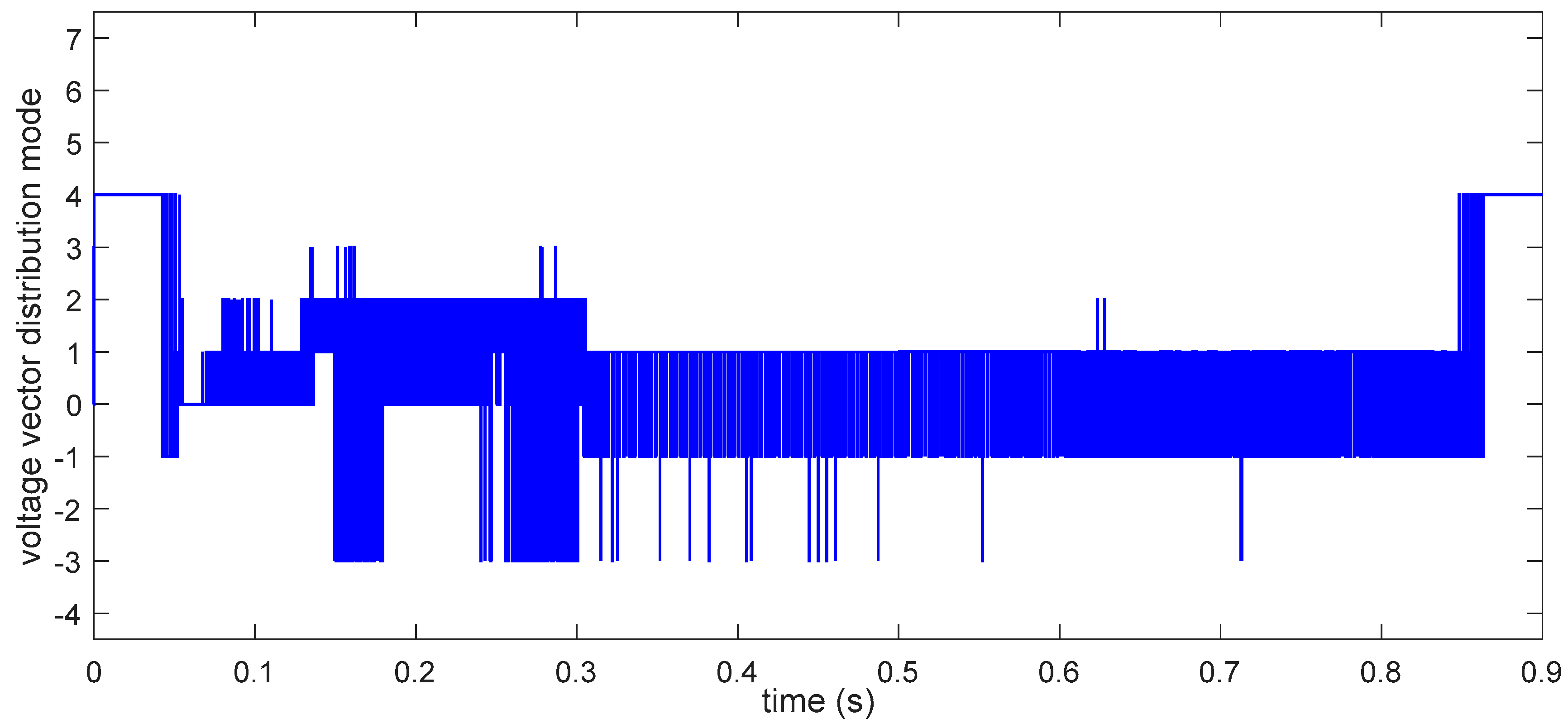
| Voltage Vector Distribution Method | Specific Circumstance | Mode Number |
|---|---|---|
| Low switching frequency method | The nth candidate vector is selected (the mode number indicates the ranking of selected vector in the sorted sequence) | 1~7 |
| Accurate power following method | inverter1’s power following deviation equals to 0 | 0 |
| inverter1’s power following deviation is not equal to 0 | −1 | |
| Linear partition method | inverter1’s power following deviation equals to 0 | −2 |
| inverter1’s power following deviation is not equal to 0, but can be integrally synthesized | −3 | |
| cannot be integrally synthesized | −4 |
© 2018 by the authors. Licensee MDPI, Basel, Switzerland. This article is an open access article distributed under the terms and conditions of the Creative Commons Attribution (CC BY) license (http://creativecommons.org/licenses/by/4.0/).
Share and Cite
Jia, Y.-F.; Chu, L.; Xu, N.; Li, Y.-K.; Zhao, D.; Tang, X. Power Sharing and Voltage Vector Distribution Model of a Dual Inverter Open-End Winding Motor Drive System for Electric Vehicles. Appl. Sci. 2018, 8, 254. https://doi.org/10.3390/app8020254
Jia Y-F, Chu L, Xu N, Li Y-K, Zhao D, Tang X. Power Sharing and Voltage Vector Distribution Model of a Dual Inverter Open-End Winding Motor Drive System for Electric Vehicles. Applied Sciences. 2018; 8(2):254. https://doi.org/10.3390/app8020254
Chicago/Turabian StyleJia, Yi-Fan, Liang Chu, Nan Xu, Yu-Kuan Li, Di Zhao, and Xin Tang. 2018. "Power Sharing and Voltage Vector Distribution Model of a Dual Inverter Open-End Winding Motor Drive System for Electric Vehicles" Applied Sciences 8, no. 2: 254. https://doi.org/10.3390/app8020254