Article

Compact Birefringent Waveplates Photo-Induced in Silica by Femtosecond Laser

1
Institut de Chimie Moléculaire et des Matériaux d'Orsay, UMR CNRS-UPSud 8182, Université de Paris Sud 11, Bâtiment 410, Orsay 91405, France
2
interdisciplinary Photonic Laboratories (iPL), School of Chemistry, The University of Sydney, Sydney, NSW 2006, Australia
*
Author to whom correspondence should be addressed.
Micromachines 2014, 5(4), 825-838; https://doi.org/10.3390/mi5040825
Submission received: 21 August 2014 / Revised: 25 September 2014 / Accepted: 26 September 2014 / Published: 30 September 2014
(This article belongs to the Special Issue Laser Micro- and Nano- Processing)

Abstract

:
Recently, we showed that femtosecond laser induced “nanogratings” consist of thin regions with a low refractive index (Δn = −0.15), due to the formation of nanoporous silica surrounded by regions with a positive index change. In this paper, we investigate a wide range of laser parameters to achieve very high retardance within a single layer; as much as 350 nm at λ = 546 nm but also to minimize the competing losses. We show that the total retardance depends on the number of layers present and can be accumulated in the direction of laser propagation to values higher than 1600 nm. This opens the door to using these nanostructures as refined building blocks for novel optical elements based on strong retardance.

1. Introduction

Current advanced femtosecond laser systems offer a myriad of possibilities to modify glassy media [1]: from surface ablation, annealing, and voids to 3D refractive index modification (positive or negative index change with isotropic or anisotropic properties) depending on the laser parameters. Recently, further unique properties of laser induced glass modifications have been discovered including orientational dependent writing [2,3,4], glass decomposition [5,6] and elemental distribution with sub-wavelength spatial resolution [7]. To our knowledge, no other technique holds the same potential for realizing 3D multi-functional photonic devices fabricated in a single step in a wide variety of transparent materials, particularly high temperature silica. It exhibits enormous potential in the development of a new generation of components for applications in micro-optics, telecommunications, 3D optical data storage, imaging, bio-photonics and many more.
A decade ago, it was shown that plasma fluctuation (plasmon modes within confined spaces) can couple to electromagnetic waves and give rise to self-organized structures in the plasma that are recorded in the material afterwards through plasma electron trapping and plasma energy absorption [7]. This was the first time that quasi-periodic sub-wavelength structures made up by the light were fabricated in volume, in contrast to 2D nanogratings produced by lasers on surfaces [8]. Recently, we showed that these nanogratings consist of thin regions with a low refractive index (typically Δn = −0.15) due to volume expansion and the formation of nanoporous silica [5,6], surrounded by homogeneous regions with a positive index change. These porous nanolayers exhibit strong uniaxial negative form birefringence (typically ~10−2) with a fast axis parallel to the polarization of the writing laser [9] and essentially arise as a result of condensation of vaporized glass within a confined but inflated volume after excitation. One of the most important parameters characterizing anisotropic optical properties of the “nanogratings” is birefringence, or retardance, where differences exist between the optical path of the slow and fast axes. Extremely large stresses and static pressures up to 10–20 GPa have recently been tentatively measured around these regions [10]; these are characteristic of extreme formation conditions that do not appear to have an analogous counterpart in nature and therefore open up a fascinating region of dynamic glass processing. Recently, Fernandes et al. have used 3D waveguides to engineer the stress-induced birefringence in the nanogratings regime [11]. This offers tunable birefringence up to 4 × 10⁻⁴, possibly enabling great flexibility in designing polarization dependent devices, as well as making polarization independent devices. So large are these combined effects that it is possible to achieve birefringence values in the range of 10−2 [9] within a 30 μm thick monolayer (i.e., a half-waveplate operating at 550 nm), possibly much more. For comparison, commercial quartz crystal exhibits a similar birefringence around 9 × 10⁻³. In addition, this offers advantages such as a low cost silica substrate with a high thermal reliability. Silica has a high laser-induced damage threshold, and the method allows the possibility of choosing on demand the neutral axis orientation to spatially vary the retardance across the structure with a resolution ranging from sub-diffraction limit (for energy just above the threshold) up to a few times larger than the laser spot size at high energy. Consequently, a series of simple and “low” retardance birefringent optical elements [12] were developed based on these porous nanolayers induced by ultrashort laser pulses in fused silica. Recent achievements include 5D optical recording [13], monolayer waveplates that act as azimuthal/radial polarization [14], optical vortex converters [15] but also waveguides retarders [16] and rotated waveplates in integrated waveguide optics [17].
In this paper, we investigate a wide range of laser parameters to achieve retardance up to a record 350 nm within a single layer and we optimized multilayers writing in order to continuously accumulate retardance in the laser propagation direction. We studied the focusing depth dependence according to the focusing conditions in order to keep high retardance and to minimize orientational writing effects. This opens the door to using these nanostructures as building blocks for novel optical elements based on strong accumulated retardance (i.e., many wavelengths) whose properties, such as slow axis orientation, can also be spatially varied in the propagation direction. For example, analogous twisted nematic liquid like crystals made in fused silica [18] that exhibit enormous advantages including broad transparency, high damage threshold and reliability.

2. Experimental Section

The direct writing procedure using IR femtosecond laser was first developed by Davis et al. [19]. Laser processing is undertaken with a femtosecond laser (1030 nm, 300 fs). The single mode output is focused below the surface (from 50 μm up to 1 mm depth) of the silica (Suprasil Type I, Heraeus Holding GmbH, Hanau, Germany) plate using three different focusing optics (0.6 NA aspheric lens, 0.35 NA and 0.55 NA microscope objectives). The vector of the beam is perpendicular to the surface of the plate. The pulse front tilt (PFT) was measured to be 0.064° (or 3fs/mm) before the microscope objective. The azimuth of the PFT was measured at an angle of 36° to the X writing direction. The sample can then be moved in three dimensions using computer-controlled stages. The linear polarization was computer-controlled using a half waveplate mounted on a rotation stage, allowing control of the photo-induced birefringence slow axis orientation. Depending on the laser scanning direction (X or Y) and the linear polarization orientation (x or y), different writing configurations noted as “Xy” (writing horizontal, i.e., X; laser polarization vertical, i.e., y) were applied.
The laser pulse energy was varied over (0.2–2.5) µJ; i.e., above the second damage threshold where porous nanolayers are formed. The scanning speed was varied from 10 to 1000 μm/s and the repetition rate from 1 kHz to 1 MHz. This allows variation of the pulse-to-pulse densities from 1 to 5 × 10⁴ pulses/micron. In the “multilayer” case, we stack birefringent layers (up to 10) that are “Z-spaced” (i.e., in the laser propagation direction noted Z) by various values ranging from 1 μm (“intricate” layers) to 50 μm (nearly independent layers). After irradiation some laser tracks have been observed using a Field-Emission Gun Scanning Electron Microscope (FEG-SEM, ZEISS SUPRA 55 VP, Carl Zeiss Microscopy GmbH, Iéna, Germany). This allows examination of uncoated insulating or dielectric specimens using low accelerating voltage (~1 kV) and very low current (a few pA). Thus, the original characteristics of the samples can be preserved for further testing or manipulation (no conductive coating is necessary).
A quantitative birefringence measurement system based on a Sénarmont compensator was used for calibration of the waveplates and for additional birefringence characterization. The Sénarmont compensator couples a highly precise quarter wavelength birefringent quartz plate with a 180-degree rotating analyzer to provide retardation measurements having an accuracy that approaches one thousandth of a wavelength (λ/1000). The device is utilized for retardation measurements over one wavelength range (up to 546 nm) for the quantitative analysis of birefringence. The higher retardance values are determined using the Michel Levy color chart with a BX60 polarized light microscope (Olympus, Tokyo, Japan) or using a spectroscopic phase modulated ellipsometer.
The losses over (185–2100 nm) of the laser-induced permanent material modification were measured with a spectrometer (rCary 5000, Varian, Palo Alto, CA, USA). UV-Vis-IR spectral retardance measurements of the waveplates were performed using a spectroscopic phase modulated ellipsometer (Uvisel ER from Horiba Jobin Yvon Inc., Palaiseau, France). This technique uses photo-elastic devices to perform the polarization modulation without any mechanical movement resulting in high signal-to-noise ratio from 180 to 2100 nm. Based on measurements of the light polarization changes upon transmission, spectroscopic ellipsometry measures the complex ratio ρ = tan(Ψ)·exp(I·Δ) as a function of the wavelength. Then we can extract the quantitative spectral retardance from those measurements using the following expression: R(λ) = Δ(λ)·λ/(2π).

3. Results and Discussion

If a converter is designed for a 1064 nm wavelength, the corresponding retardance values for quarter- and half-wave plates are 267 and 532 nm, respectively. In order to reduce the fabrication time we have performed a set of experiments searching for laser writing conditions to obtain the highest retardance within a single scan. The quantitative retardance at 546 nm was measured and compared with images of related porous nanogratings (using FEG-SEM) by varying the repetition rate (from 1 kHz up to 1 MHz), the scanning velocity (from 10 up to 1000 μm/s; i.e., the number of pulses per μm), the pulse energy (from 0.2 up to 2.5 μJ), but also the focus depth (from 20 up to 1000 μm) covering many stacked layers. The threshold for porous nanoplanes formation (and related form birefringence) was around 0.15 μJ and is independent of the writing speed and repetition rate provided that enough pulses have been accumulated (typically more than 100 pulses/μm). Notice that only positive index changes (expected from defects centers and densification) and related stress birefringence (consistent with the material elastic response [10]) was observed for exposures below 10 pulses/μm. This threshold slightly increases to 0.25 μJ for deep focusing (typically greater than 500 μm deep). Whatever the repetition rate, the retardance shows a trend to saturation with decreasing scanning speed (i.e., for 1000 pulses/μm). This can be understood taking into account the mechanism (O2 migration and nanoporous silica formation arising from condensation under confinement stresses inside nanolayers [5]). Quantitatively, the major part of the birefringence is due to form birefringence [B] even if a significant part (up to 20%) is related to stress birefringence. We consider that [B] is proportional to the number of nanoplanes, their spacing, and to the amount of glass decomposition (i.e., the porosity filling factor) within nanoplanes. Assuming a direct relationship between the generation of self-trapped-excitons (STEs) and glass breakdown, the amount of decomposition will be proportional to the branching ratio (ε) from self-trapped-excitons (STE), on the one hand, and to STE concentration on the other hand ([STE]) which are produced by a series of pulses (np). Therefore, we may write [B] ≈ np × ε × [STE] where the STE concentration exhibits a trends to saturation with increasing number of pulses [20]. In contrast the retardance increases with the pulse energy (due to a decrease of the nanoplanes spacing and to an increase of the length of the laser tracks) and reaches a certain saturation value (its level depends on the repetition rate and the glass chemical composition).
The optimal repetition rate to achieve the highest retardance values (up to 350 nm in a single layer) is around 10–100 kHz [21]. The lower retardance values (typically below 150 nm) observed for repetition rates higher than 100 kHz (as shown in [21,22]) could be explained by thermal accumulation that deteriorates the “quality” of the nanogratings. These become disrupted as can be observed on SEM images in Figure 1a, in agreement with [22]. Finally, using the following set of parameters 1030 nm, 300 fs, 0.6 NA, 100 kHz, 100–500 μm/s, 1–2.5 μJ/pulse and with the quantitative birefringence measurements, we confirm the successful realization of a very high retardance of about 350 nm (100 μm/s, 2.5 μJ/pulse) at λ ~ 546 nm wavelength—this is the highest reported value in the literature using this direct writing technique. These results obviously indicate that the evolution of retardance can be controlled as a function of laser parameters.

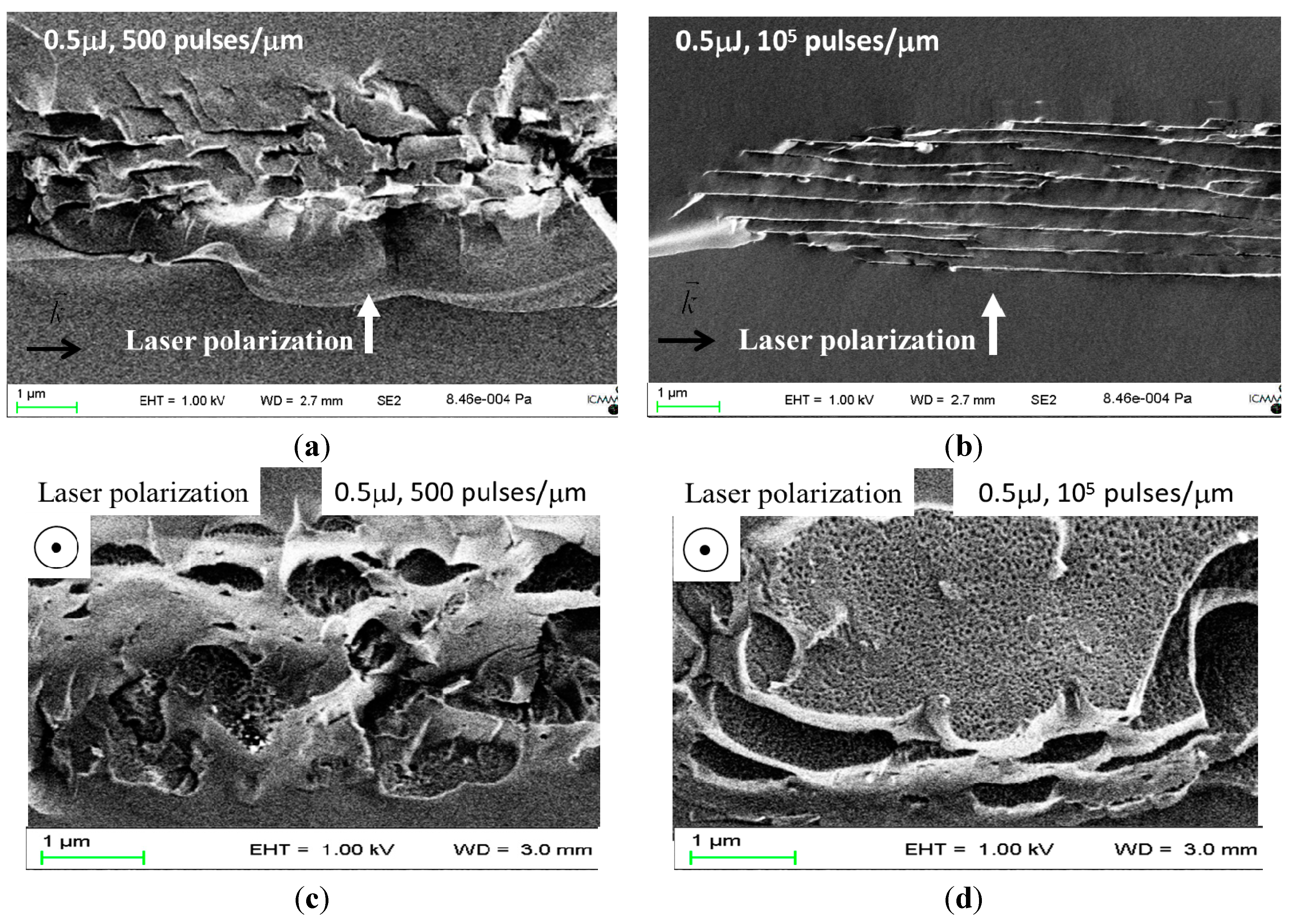
3.1. Minimizing Diffraction and Light Scattering

In the second part of this work, we investigate the problem of the undesired diffraction pattern that can be observed due to the arrangement of the laser tracks. At first, we wrote “uniform” waveplates of dimensions 1 mm × 1 mm by successively writing 1 mm long lines separated by a few microns at a speed of 500 μm/s and with a repetition rate of 500 kHz. However, since the lines did not overlap to produce a homogeneous pattern, an undesired diffraction pattern can be observed due to the arrangement of the lines. To minimize diffraction effects related to the formation of a thick Bragg grating, the spacing L between adjacent lines was varied from 0.5 up to 5 μm. To measure the diffraction pattern, a mechanically chopped TEM00 He-Ne probe beam direction was tuned to the Bragg external angle θBragg in order to get the phase-matching conditions leading to a maximum in the diffraction efficiency (sin θBe = λ/2Λ). By measuring the diffraction efficiency η = I1/I0 of the gratings (where I1 is the diffracted power in the first order and I0 the incident power of the He-Ne beam), we determined that 0.5 or 1 μm spacing allows suppression of this diffraction grating effect and ensures “homogenous” squares but leads also to higher retardance that is likely due to cumulative stress [23] arising from anisotropic shape of the confinement volume. Notice that recently, this stress-induced birefringence has been successfully engineering in femtosecond laser fabricated waveguides in fused silica [11]. In addition, the measurement of these thick Bragg holograms angular acceptances ΔθB (ΔθB ≈ 2Λ/teff) allow the determination of the effective thickness, teff, that is estimated to be around 30 μm for the conditions that achieve strong retardance (e.g., 250 nm @ λ = 546 nm) and thus a birefringence as high as B ~ (0.80 ± 0.05) × 10−2. The relative scattering was characterized at 632.8 nm from the average of five measurements of illuminance broadcast at a distance D = 20 cm from the component with a photodiode placed midway between the order 0 and order 1 of the forward diffraction gratings (if any). Since the light scattering from the nanogratings differs strongly in forward and backward directions and the angular intensity can be changed with changes in writing parameters, this provides qualitative measurements of the light scattering. These measurements are used as an on-line diagnostic in order to minimize the forward light scattering according to the selected laser writing parameters. The results can be summarized as follows: the scattering coefficient is lower by a factor 4 for Xx configuration when compared to Yx and Yy configurations. The lower the lens NA, the lower is the scattering. Typically, for a similar retardance level, the scattering is twice smaller for a 0.16 NA when compared to 0.6 NA aspheric lens. For a 0.6 NA aspheric lens the scattering increases by a factor 2 from 0.5 μJ up to 1 μJ, then it exhibits a trend to saturation up to 1.5 μJ and then it increases dramatically for higher pulse energies that correspond to disrupted nanogratings microstructure. We speculate that the scattering losses are introduced by nanoporous glass observed inside the nanoplanes with characteristic dimensions of few tens of nanometers [5]. The scattering losses also tend to be smaller for the structures written with lower translation speed (more pulses per micron). As shown in Figure 1a,b, this is likely due to the nanogratings that evolve from disrupted nanoplanes (see Figure 1a) to a well-organized nearly periodic grating (Figure 1b) when increasing the number of pulses from 500 pulses/μm to 104 pulses/μm. Another possibility could be the decrease of the average pore size within the nanoplanes that we observed in these conditions as shown in Figure 1c,d.
Figure 1. FEG-SEM (Field-Emission Gun Scanning Electron Microscope) secondary electron images of laser track cross-section for the writing laser polarization (a, b) perpendicular to the scanning direction and (c, d) parallel to the scanning direction. The laser parameters were: 0.5 μJ/pulse, 1030 nm, 300 fs and 500 kHz. A focusing aspheric lens of 0.6 NA was used.
Micromachines 05 00825 g001

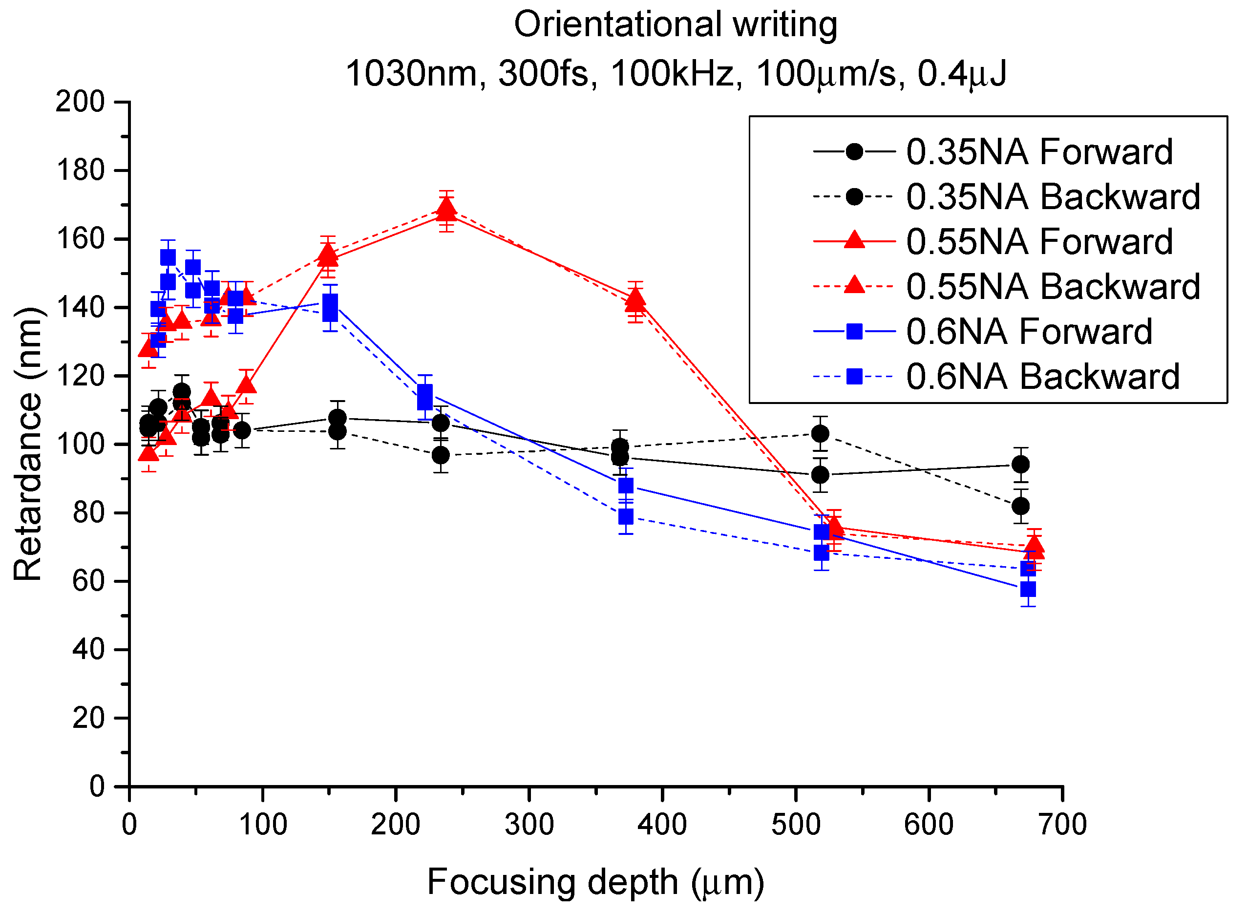
3.2. Minimizing the Orientational Writing Effect

Another related problem needs consideration: scanning in both directions is anisotropic and results in an inhomogeneous pattern due to the so-called “Quill writing effect” [2,3,4]. The directional dependence of written lines was observed when the laser beam polarization was either parallel or perpendicular to the writing direction. In addition the imprinted lines can be themselves asymmetric [3] resulting in non-homogenous retardance profile within the line itself (e.g., one edge exhibit higher retardance compared to the other one). Reversing the scanning direction correspondingly reversed this feature. Consequently, the lines did not overlap homogeneously thus degrading the quality of the produced waveplate. As a result of this asymmetry, the written tracks “join” together differently depending on the writing direction. To avoid this effect, the waveplates can be written by scanning in only one direction but this significantly increases the total processing time. Instead, we have determined the laser writing conditions and the writing configuration that allows minimization of the quill writing effect. Reported elsewhere [3], we determined that Xx configuration is the most suitable writing configuration and using specific laser conditions avoids any quill writing effect, resulting in more homogenous waveplates. To avoid this problem regardless of the focusing depth, changes in the orientational dependence by adjusting the numerical aperture and the type of focusing optics was studied. Figure 2 shows the retardance for two scanning directions (+X and −X) changing the focusing depth up to 700 μm. We investigated 3 different focusing objectives: a 0.6 NA aspheric lens, a 0.55 NA microscope objective and a 0.35 NA microscope objective. As can be seen in Figure 2, the use of aspheric lens or low NA objective minimizes the orientational writing effect. In contrast a 0.55 NA microscope objective enhances this effect, in particular for low focusing depth (typically below 200 μm).
Figure 2. Influence of the focusing depth of the orientational writing effect for fixed pulse energy of 0.4 μJ/pulse (full lines for the forward +X direction and dotted lines for backward −X direction). The parameter of the study is the kind of focusing optics: 0.6 NA aspheric lens (blue curve), 0.35 NA microscope objective (black curve) and 0.55 NA microscope objective (red curve). The others laser parameters are as follows: 1030 nm, 300 fs, 100 kHz, 100 μm/s, and polarization parallel to the scanning direction (Xx configuration).
Micromachines 05 00825 g002

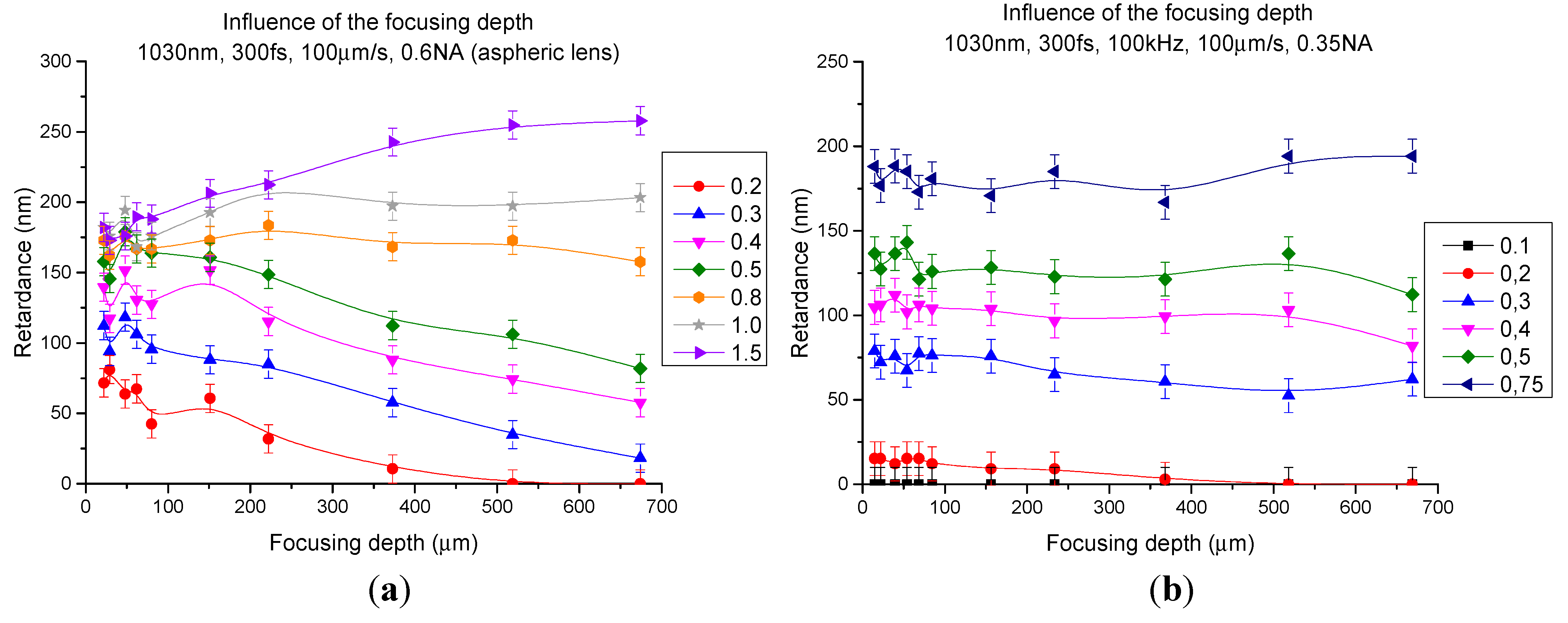
3.3. Minimizing the Focusing Depth Dependence in Order to Write Multilayer Waveplates

There is a balance required between the desired high retardance and the least number of layers in the propagation direction. Much literature have reported the following two phenomena when focusing inside a material: (1) self-focusing when the pulse energy exceeds the threshold (0.35 μJ/pulse in silica), and (2) spherical aberration which increases with focus depth. In contrast, it is known that spherical aberration is present with strong focusing as a result of the refractive index mismatch at the interface of two transparent media. However, in this case the deeper the geometrical focus penetrates into the bulk of the sample, the stronger the beam is distorted and elongated. Mostly, this effect is undesired as it strongly distorts the intensity distribution in the focus and this will affect the photo-induced retardance written at different depths, which is usually detrimental for multilayer applications. However, spherical aberrations can be well controlled using adaptive optics. This maintains consistent focusing quality and also may offer further degrees of control for tuning and shaping retardance effects based on nanogratings as reported recently in [24].
The depth dependence of the retardance was studied using three different kinds of focusing optics: a 0.6 NA aspheric lens, a 0.55 NA Olympus microscope objective and a 0.35 NA Olympus microscope objective. In the following experiments the geometrical focus was moved from the surface down to 700 μm into the bulk of the silica. The retardance was then recorded according to the focusing depth for various objectives and various pulse energies as shown in Figure 3. With a 0.6 NA aspheric lens, it depends on the pulse energy. Below 0.5 μJ/pulse, the retardance decreases linearly for deeper focusing penetration. For medium energies around (0.8–1) μJ/pulse the measurements demonstrated that we managed to keep a constant retardance from 50 μm up to 700 μm. This is likely due to a balance between the occurrence of self-focusing effects and spherical aberration even when the focus goes very deep. Then at higher energies, the retardance increases linearly with the focusing depth. This clearly demonstrates the strong influence of spherical aberration on the laser writing process at this relatively high numerical aperture. In this case, the deeper the geometrical focus is moved into the bulk of the sample, the stronger the beam is distorted and elongated. The retardance of the birefringent structure is a product of refractive index difference multiplied by the length of the structure. As a result, one way to increase the induced retardance is the introduction of strong spherical aberration provided that the energy is high enough to induce nanogratings.
Figure 3. Influence of the focusing depth of the laser induced retardance for various pulse energies for (a) 0.6 NA aspheric lens and (b) 0.35 NA microscope objective. The others laser parameters are as follows: 1030 nm, 300 fs, 100 kHz, 100 μm/s, and polarization parallel to the scanning direction (Xx configuration).
Micromachines 05 00825 g003
According to the literature, another way is to reduce the NA since the lower the numerical aperture is the longer the structure. Additionally, lower NA results in a bigger spot size that is important for producing homogeneous waveplates in a reasonable amount of time. This approach has been applied to get ~300 nm retardance by using 0.1–0.2 NA objective [25]. However, as shown in Figure 3b, we do not observed higher retardance using 0.35 NA rather than 0.6 NA. In addition, with the 0.35 NA objective, the measurements demonstrated that we managed to keep a constant retardance from 50 μm up to700 μm by keeping the pulse energy at a constant value up to 0.75 μJ.

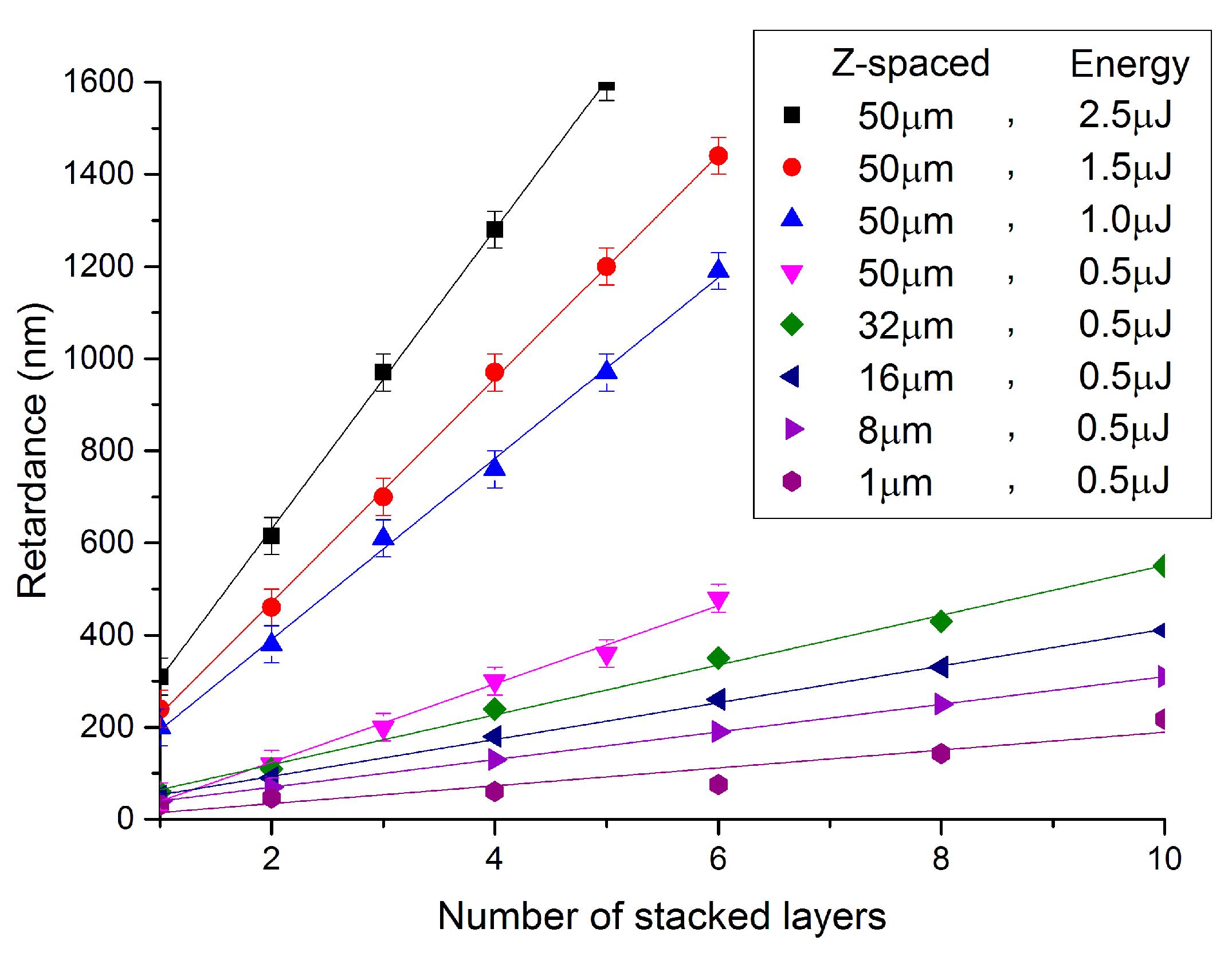
3.4. Stacking Birefringent Layers

Based on the above reported results, homogenous single layer quarter and half waveplates operating up to 532 nm were thus written respectively using the following set of parameters: (100 kHz, 500 μm/s, 1 μJ) and (100 kHz, 200 μm/s, 2 μJ). Currently, during the recording procedure the retardance can be controlled with a target retardance accuracy of about 10 nm, while the slow axis angle can be defined with a precision of a few degrees. Finally, the writing time of a 1 mm² waveplate was around 1 h, which can be significantly reduced to a few minutes (e.g., by scanning at 10 mm/s as shown in [25]) and even less by further optimizing the laser processing parameters or using advanced shaping strategies such as multipoint writing [26].
For specific components like twisted waveplates or multiple order waveplates, the required strong retardance (typically 1500 nm) can be achieved by stacking several birefringent layers together, while using the same focusing optics (namely aspheric lens or low NA microscope objective) and laser power as for elements operating at λ = 532 nm (though there is no wavelength restriction in principle). Therefore, for the third part of this paper, we investigate the possibility of accumulating retardance by stacking birefringent laser tracks. As can be seen in Figure 4, the phase retardance can be tuned by stacking birefringent laser tracks with different number of layers (up to 10) “Z-spaced” by various values ranging from 1 μm (“intricate” layers) up to 50 μm (nearly independent layers). The retardance value increase linearly with the number of stacking layers and their Z-spacing but the slope strongly depends on the layers spacing and also on the laser pulse energy. As shown in Figure 1, FEG-SEM images were performed where the femtosecond laser polarization was perpendicular to the scanning direction. Under these conditions, the thickness of a 250 nm retardance monolayer (i.e., the length of the nanogratings area) is around 35 μm and it can be seen that stacking layers can increase birefringent region thickness. The related retardance increases linearly with the thickness whereas the calculated birefringence (i.e., retardance divided by the layer thickness) remains constant and on the order of B ≈ 7 × 10⁻³. Using a Z-spacing of 50 μm, we show the possibility of accumulating more than 1500 nm of optical phase retardance using only 5 layers. For comparison, to obtain similar retardance in quartz requires a 150 μm thick crystalline quartz plate. Notice that birefringence as high as (1.75 ± 0.15) × 10−2 can be obtained using, for example, the following writing conditions: (1030 nm, 300 fs, 0.6 NA, 500 kHz, 500 μm/s, 1 μJ/pulse) in silica but at the expense of higher losses (both scattering and absorption related to defects centers, as shown in Figure 5).
In addition it should be noted that when stacking individual layers accumulated stress could be an additional problem. This can lead to cracks or overlaps between stress-induced birefringence and form birefringence leading to non-uniformity. To avoid cracks we have thus written the multilayers waveplates in thick samples (at least 3 mm instead of 1 mm for single layer). In addition, in some case we have performed an annealing treatment (typically 3 h at 700 °C) to relax the accumulated stress (and to bleach most of the photo-induced defects centers as described in the next section).
Figure 4. Retardance according to the number of stacked layers and their Z-spacing (spacing between consecutive layers in the propagation direction) for various pulse energies (1030 nm, 300 fs, 100 kHz, 100 μm/s, 0.6 NA, polarization parallel to the scanning direction).
Micromachines 05 00825 g004
Figure 5. (a) Losses for a group of half (1/2) and quarter (1/4) waveplates samples. The full line are for the waveplates without any further treatment and the dotted lines are after annealing the waveplates at 600 °C for 2 h. (b) Spectral retardance dependence before and after annealing measured with the ellipsometer. The target retardance values were a half and a quarter of 532 nm.
Micromachines 05 00825 g005

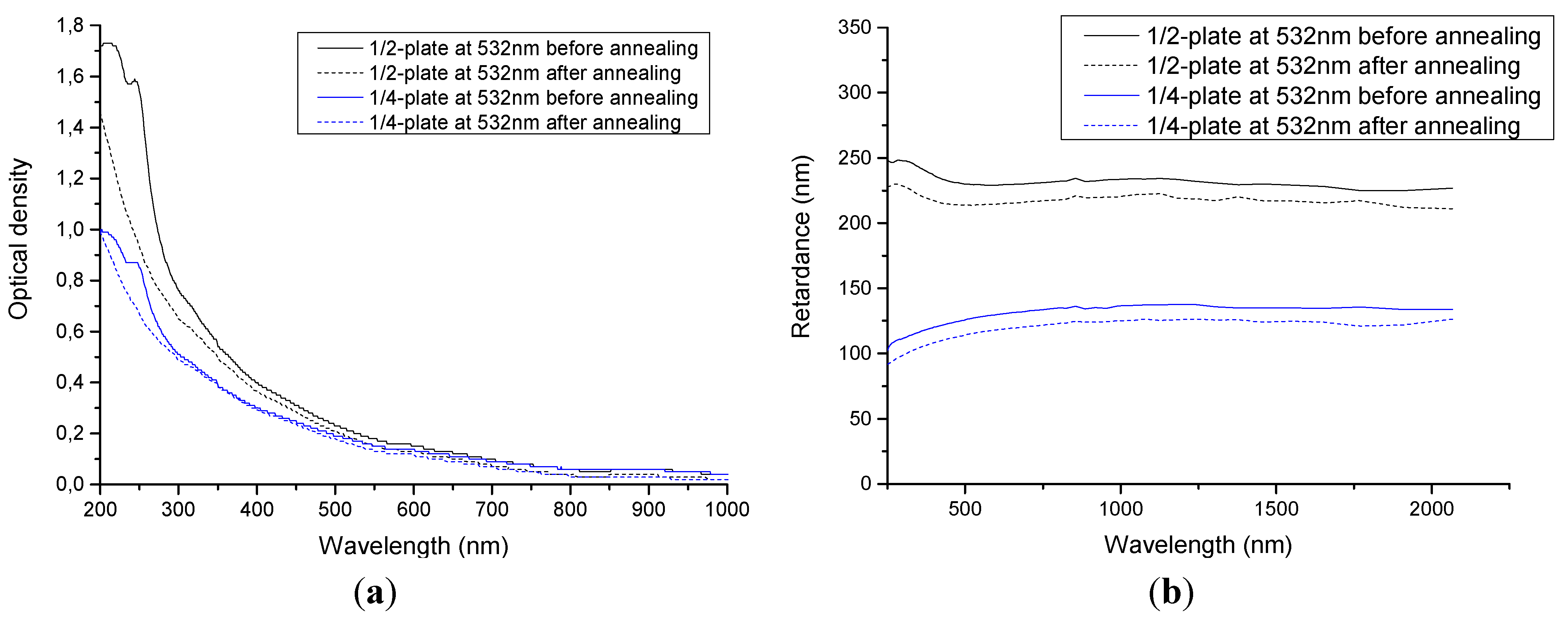
3.5. Loss and Birefringence Dispersion

The main part of the laser-induced losses observed for Type II modification is likely due to the light scattering of the inhomogeneous nanostructure (porous nanoplanes) [5]. Additionally, two intense absorption bands can be distinguished at short wavelengths, which are attributed to SiE’ centers at 210 nm (≡Si, an unpaired electron in a silicon atom bound to three oxygen atoms), and oxygen deficiency center (ODC)(II) at 245 nm, (–O–Si–O–, a divalent silicon atom) [27,28]. A detailed description of their formation mechanism is given in [29]. In addition the absorption measurements of the sample after annealing at 600 °C for 2 h clearly indicated complete erasure of the E’ and ODC(II) defects if attributed to the absorption bands observed at 210 and 240 nm, respectively (Figure 5a). The erasure of the defects resulted in significantly lower losses from 200 to 400 nm. Nevertheless, we estimated that about 50% of the incident light is scattered at UV wavelengths < 300 nm for a 1/2-waveplate designed for 266 nm laser light. In the visible, however, no major improvement in optical quality was observed after the thermal treatment. The final losses are estimated to be around 30% for a 532 nm 1/2-waveplate and 10% for a 1064 nm 1/2-waveplate and less than 4% for a 1550 nm 1/2-waveplate.
The retardance variation was measured from 250 to 2100 nm using an ellipsometer. The measurements on the short wavelength side were limited by the nanogratings spacing as predicted by effective medium theory. The retardance spectral dependence shows a plateau extending to at least 2.1 μm (Figure 5b). The long plateau tail is expected as at longer wavelengths the retardance approaches asymptotically to the value predicted by the refractive index effective medium theory. The annealing decreased the retardance value only by 5% and that is likely due to stress relaxation. This indicates that annealing defects should improve the transparency of nanogratings based birefringent elements at wavelengths shorter than 300 nm without significantly impacting on the birefringence.

4. Conclusions

Recently, a series of simple monolayer birefringent optical elements were developed based on self-assembled nanostructures induced by ultrashort laser pulses in fused silica. Such recent achievements include long lifetime 3D optical data recording, radial/azimuthal polarization and optical vortex converters. Here, we demonstrated that these nanostructures can be accumulated along the propagation direction with nanoscale control. These can be used as the building blocks for novel optical elements based on highly precise and strongly accumulated optical retardance. The developed multiple order waveplate can be seen as a demonstration of Z-spatially birefringent element fabrication (a silica analog of a twisted nematic liquid crystals where there is a constant value of retardance with the continuously varying direction of the slow axis in the z direction). Both ¼ and ½ waveplates and combinations therefore are readily fabricated, allowing total integration of birefringent components and waveguides with unprecedented precision and resolution. These silica waveplates exhibit enormous advantages including a broad spectral range from UV to IR and high thermal stability (no decay after 2 h @ 1000 °C [30] from which an estimated lifetime of about 300 million years at room temperature) can be obtained. This is primarily due to the intrinsic structures (nanoporous silica) and the absence of glued components found in commercial waveplates, and a much higher damage threshold (25 ± 3 J/cm², at λ = 1064 nm, 3.5 ns, 10 Hz [31]). In conclusion, these results are achieved because waveplates are fabricated using nanoporous silica layers, a regime between molecular processing and nanoscale milling. The major remaining problem is strong scattering, which can introduce large losses in the UV-Vis range. These can be partly reduced by writing weaker and longer structures but also by engineering the porosity dimensions and shape at the root of the nanograting’s refractive index contrast.

Acknowledgments

This work has been performed in the frame of Femtosecond Laser Application in Glasses (FLAG) consortium project with the support of several organizations: the Agence Nationale pour la Recherche (ANR-09-BLAN-0172-01), the RTRA Triangle de la Physique (Réseau Thématique de Recherche Avancée, 2008-056T) and FP7-PEOPLE-IRSES e-FLAG 247635. Support from the Australian Research Council (ARC) through grants ARC FT110100116 and DP120104035 are acknowledged.

Author Contributions

Matthieu Lancry and Bertrand Poumellec conceived, devised and helped carry out the experiments, wrote the paper. Kevin Cook and Rudy Desmarchelier asssisted the experiments and edited the paper. John Canning helped interpret some of the experimental data, edit the paper and suggest some new directions.

Conflicts of Interest

The authors declare no conflict of interest.

References

  1. Itoh, K.; Watanabe, W.; Nolte, S.; Schaffer, C.B. Ultrafast processes for bulk modification of transparent materials. MRS Bull. 2006, 31, 620–625. [Google Scholar] [CrossRef]
  2. Kazansky, P.G.; Yang, W.; Bricchi, E.; Bovatsek, J.; Arai, A.; Shimotsuma, Y.; Miura, K.; Hirao, K. “Quill” writing with ultrashort light pulses in transparent materials. Appl. Phys. Lett. 2007, 90, 151120. [Google Scholar] [CrossRef]
  3. Poumellec, B.; Lancry, M.; Desmarchelier, R.; Hervé, E.; Brisset, F.; Poulin, J. Asymmetric Orientational Writing in glass with femtosecond laser irradiation. Opt. Mater. Express 2013, 3, 1586–1599. [Google Scholar] [CrossRef]
  4. Yang, W.; Kazansky, P.; Svirko, Y. Non-reciprocal ultrafast laser writing. Nat. Photonics 2008, 2, 99–104. [Google Scholar] [CrossRef]
  5. Lancry, M.; Poumellec, B.; Canning, J.; Cook, K.; Poulin, J-C; Brisset, F. Ultrafast nanoporous silica formation driven by femtosecond laser irradiation. Laser Photonics Rev. 2013, 7, 953–962. [Google Scholar]
  6. Canning, J.; Lancry, M.; Cook, K.; Weickman, A.; Brisset, F.; Poumellec, B. Anatomy of a femtosecond laser processed silica waveguide [Invited]. Opt. Mater. Express 2011, 1, 998–1008. [Google Scholar] [CrossRef]
  7. Shimotsuma, Y.; Kazansky, P.; Qiu, J.; Hirao, K. Self-organized nanogratings in glass irradiated by ultrashort light pulses. Phys. Rev. Lett. 2003, 91, 247405. [Google Scholar] [CrossRef]
  8. Birnbaum, M. Semiconductor Surface Damage Produced by Ruby Lasers; Aerospace Corp: EL Segundo, CA, USA, 1966. [Google Scholar]
  9. Bricchi, E.; Klappauf, B.G.; Kazansky, P.G. Form birefringence and negative index change created by femtosecond direct writing in transparent materials. Opt. Lett. 2004, 29, 119–121. [Google Scholar] [CrossRef]
  10. Champion, A.; Beresna, M.; Kazansky, P.; Bellouard, Y. Stress distribution around femtosecond laser affected zones: Effect of nanogratings orientation. Opt. Express 2013, 21, 24942–24951. [Google Scholar] [CrossRef]
  11. Fernandes, L.A.; Grenier, J.R.; Herman, P.R.; Aitchison, J.S.; Marques, P.V. Stress induced birefringence tuning in femtosecond laser fabricated waveguides in fused silica. Opt. Express 2012, 20, 24103–24114. [Google Scholar] [CrossRef]
  12. Cheng, G.; Mishchik, K.; Mauclair, C.; Audouard, E.; Stoian, R. Ultrafast laser photoinscription of polarization sensitive devices in bulk silica glass. Opt. Express 2009, 17, 9515–9525. [Google Scholar] [CrossRef]
  13. Zhang, J.; Geceviçius, M.; Beresna, M.; Kazansky, P.G. 5D data storage by ultrafast laser nanostructuring in glass. In Proceedings of CLEO: Science and Innovations, San Jose, CA, USA, 9–14 June 2013.
  14. Beresna, M.; Geceviçius, M.; Kazansky, P.G. Polarization sensitive elements fabricated by femtosecond laser nanostructuring of glass [Invited]. Opt. Mater. Express 2011, 1, 783–795. [Google Scholar] [CrossRef]
  15. Beresna, M.; Geceviçius, M.; Kazansky, P.G.; Gertus, T. Radially polarized optical vortex converter created by femtosecond laser nanostructuring of glass. Appl. Phys. Lett. 2011, 98, 201101. [Google Scholar] [CrossRef]
  16. Fernandes, L.A.; Grenier, J.R.; Herman, P.R.; Aitchison, J.S.; Marques, P.V. Femtosecond laser writing of waveguide retarders in fused silica for polarization control in optical circuits. Opt. Express 2011, 19, 18294–18301. [Google Scholar] [CrossRef]
  17. Corrielli, G.; Crespi, A.; Geremia, R.; Ramponi, R.; Sansoni, L.; Santinelli, A.; Mataloni, P.; Sciarrino, F.; Osellame, R. Rotated waveplates in integrated waveguide optics. Nat. Commun. 2014, 5, 4249. [Google Scholar] [CrossRef]
  18. Zimmermann, F.; Richter, S.; Vetter, C.; Doring, S.; Tunnermann, A.; Nolte, S. Ultrashort pulse-induced nanogratings: Temperature stable optically active phase elements. In Proceedings of 2013 Conference on Lasers and Electro-Optics Europe and International Quantum Electronics Conference, Munich, Germany, 12–16 May 2013.
  19. Davis, K.M.; Miura, K.; Sugimoto, N.; Hirao, K. Writing waveguides in glass with a femtosecond laser. Opt. Lett. 1996, 21, 1729–1731. [Google Scholar] [CrossRef]
  20. Richter, S.; Jia, F.; Heinrich, M.; Döring, S.; Peschel, U.; Tünnermann, A.; Nolte, S. The role of self-trapped excitons and defects in the formation of nanogratings in fused silica. Opt. Lett. 2012, 37, 482–484. [Google Scholar] [CrossRef]
  21. Lancry, M.; Desmarchelier, R.; Zimmermann, F.; Guth, N.; Brisset, F.O.; Nolte, S.; Poumellec, B. Porous nanogratings and related form birefringence in silicate and germanate glasses. In Proceedings of Bragg Gratings, Photosensitivity, and Poling in Glass Waveguides, Barcelona, Spain, 27–31 July 2014.
  22. Corbari, C.; Champion, A.; Geceviçius, M.; Beresna, M.; Bellouard, Y.; Kazansky, P.G. Femtosecond versus picosecond laser machining of nano-gratings and micro-channels in silica glass. Opt. Lett. 2013, 21, 3946–3958. [Google Scholar]
  23. Geceviçius, M.; Beresna, M.; Zhang, J.; Yang, W.; Takebe, H.; Kazansky, P.G. Extraordinary anisotropy of ultrafast laser writing in glass. Opt. Lett. 2013, 21, 3959–3968. [Google Scholar]
  24. Hasegawa, S.; Hayasaki, Y. Holographic vector wave femtosecond laser processing. Int. J. Optomechatron. 2014, 8, 73–88. [Google Scholar] [CrossRef]
  25. Beresna, M.; Geceviçius, M.; Lancry, M.; Poumellec, B.; Kazansky, P. Broadband anisotropy of femtosecond laser induced nanogratings in fused silica. Appl. Phys. Lett. 2013, 103, 131903. [Google Scholar] [CrossRef]
  26. Jesacher, A.; Booth, M.J. Parallel direct laser writing in three dimensions with spatially dependent aberration correction. Opt. Lett. 2010, 18, 21090–21099. [Google Scholar]
  27. Lancry, M.; Poumellec, B.; Desmarchelier, R.; Bourguignon, B. Oriented creation of anisotropic defects by IR femtosecond laser scanning in silica. Opt. Mater. Express 2012, 2, 1809–1821. [Google Scholar] [CrossRef]
  28. Sun, H.B.; Juodkazis, S.; Watanabe, M.; Matsuo, S.; Misawa, H.; Nishii, J. Generation and recombination of defects in vitreous silica induced by irradiation with a near-infrared femtosecond laser. J. Phys. Chem. B 2000, 104, 3450–3455. [Google Scholar] [CrossRef]
  29. Lancry, M.; Groothoff, N.; Poumellec, B.; Guizard, S.; Fedorov, N.; Canning, J. Time-resolved plasma measurements in Ge-doped silica exposed to infrared femtosecond laser. Phys. Rev. B 2011, 84, 245103. [Google Scholar] [CrossRef]
  30. Bricchi, E.; Kazansky, P.G. Extraordinary stability of anisotropic femtosecond direct-written structures embedded in silica glass. Appl. Phys. Lett. 2006, 88, 111119. [Google Scholar] [CrossRef]
  31. Beresna, M. Polarization Engineering with Ultrafast Laser Writing in Transparent Media; University of Southampton: Southampton, UK, 2012. [Google Scholar]

