Review

Integrated Magnetic MEMS Relays: Status of the Technology

by
Giuseppe Schiavone
1,2,*,
Marc P. Y. Desmulliez
2 and
Anthony J. Walton
1
1
Scottish Microelectronics Centre, Institute for Integrated Micro and Nano Systems, School of Engineering, The University of Edinburgh, King's Buildings, Edinburgh EH9 3JF, UK
2
Research Institute of Signals, Sensors and Systems, School of Engineering & Physical Sciences, Heriot-Watt University, Edinburgh EH14 4AS, UK
*
Author to whom correspondence should be addressed.
Micromachines 2014, 5(3), 622-653; https://doi.org/10.3390/mi5030622
Submission received: 17 June 2014 / Revised: 24 July 2014 / Accepted: 19 August 2014 / Published: 29 August 2014

Abstract

:
The development and application of magnetic technologies employing microfabricated magnetic structures for the production of switching components has generated enormous interest in the scientific and industrial communities over the last decade. Magnetic actuation offers many benefits when compared to other schemes for microelectromechanical systems (MEMS), including the generation of forces that have higher magnitude and longer range. Magnetic actuation can be achieved using different excitation sources, which create challenges related to the integration with other technologies, such as CMOS (Complementary Metal Oxide Semiconductor), and the requirement to reduce power consumption. Novel designs and technologies are therefore sought to enable the use of magnetic switching architectures in integrated MEMS devices, without incurring excessive energy consumption. This article reviews the status of magnetic MEMS technology and presents devices recently developed by various research groups, with key focuses on integrability and effective power management, in addition to the ability to integrate the technology with other microelectronic fabrication processes.

Graphical Abstract

1. Introduction

The microfabrication of magnetic structures for the production of integrated switching components has been a topic of great interest in academic institutions and the commercial world. This development has mostly been driven by the goals of producing devices that can achieve higher performance at a lower cost and with reduced footprint [1,2,3,4,5,6].
Magnetic switching offers many benefits when compared to other actuation schemes for microelectromechanical systems (MEMS). The advantages include the generation of forces with a higher magnitude and longer range [7]. This enables devices to be designed with larger contact gaps, and therefore better isolation in the OFF state, and/or with stiffer mechanical structures, which offer greater robustness to stiction, wear and other failure mechanisms. Magnetic actuation can be achieved by exciting soft magnetic microstructures employing magnets or microcoils. However, the use of external permanent magnets or embedded hard magnetic microstructures is problematic when considering direct integration with standard Integrated Circuit (IC) processing. Microcoils, on the other hand, are compatible with IC fabrication, albeit with a significant level of added complexity, but their operation requires a constant current feed. Novel designs and technologies are therefore sought to enable the use of magnetic switching architectures in integrated MEMS devices, without incurring excessive power consumption. This can be achieved by integrating latching mechanisms that hold the switched structures in the actuated state with zero constant power dissipation.
This article presents an updated review of the status of magnetic technologies for MEMS switches, and compares relevant devices recently reported in the literature, with particular focus on the key issues of their integration and effective power management. The advantages of MEMS relays in general over solid state switches are first presented, followed by an analysis of the most common failure mechanisms affecting MEMS actuators of all sorts. The desirability of magnetic architectures is then discussed, complete with their challenges and reported research efforts focused on solving the associated problems. Finally a review of recently developed devices is presented, with discussions on the advances towards the goals of full integration with low power dissipation.

2. MEMS Switches

Microelectromechanical switches are substantially different from P-type/Intrinsic/N-type (PIN) semiconductor diode or Field Effect Transistor (FET) switches, although the purpose of both types of devices is to vary the impedance of an electrical path in a controlled fashion. While solid state devices employ electric fields to vary the conductivity of a channel, effectively closing or opening a conduction line, MEMS switches utilize mechanically moving parts to physically vary the distance between two conductive elements of a signal line in order to make or break an ohmic contact (in the case of ohmic switches), or to increase or decrease the enclosed capacitance (in the case of capacitive switches). Various examples of MEMS switches in ohmic and capacitive configuration are reported in Section 2.3 and Figure 1 illustrates the two different switching principles.
MEMS switches are comprised of an actuation section and an electrical element, which can be categorized according to the actuation scheme (electrostatic, magnetostatic, piezoelectric or thermal), the geometrical configuration (vertical or horizontal actuation, beams, membranes, cantilevers, etc.), or the electrical configuration (ohmic contact or capacitive switches, series or shunt circuit architectures).
Figure 1. Switching principles for ohmic and capacitive devices.
Micromachines 05 00622 g001
Regardless of the specific design, MEMS relays generally offer a number of advantages over solid state devices such as higher OFF-state isolation for high frequency switched signals and low power consumption, depending on the actuation scheme [8]. On the other hand, MEMS switches suffer from a series of problems in terms of reliability, particularly exacerbated by failure mechanisms such as self-actuation, stiction, electromigration, microwelding, etc. [9]. MEMS devices additionally carry the burden of needing an appropriate packaging solution that guarantees functionality and reliability, which potentially increases manufacturing costs. All of these challenges are currently subjects for process improvements and optimization.

2.1. Advantages of MEMS Switches Over Solid State Switches

A comprehensive review of the status of the Radio Frequency (RF) MEMS switches technology up to the year 2003 has been published by Rebeiz, G.M. [8,10]. This section reviews the most relevant benefits of MEMS switches over solid state devices by including updated information from the literature published in the following years.

2.1.1. Low Power Consumption

Electrostatic actuation mechanisms are usually devised in the form of capacitors with movable plates, designed in a variety of shapes and configurations. By applying a voltage across the structure, a force is applied that attracts the capacitor plates together and thus creates a movement that can be exploited to switch an independent signal path. Once actuated, these devices consume minimal power to hold this state, as a dynamic current flow occurs exclusively during actuation [11], with typical overall power consumption resulting from charging and leakages of 0.05 to 0.1 mW [12]. In the case of thermal [13,14] and electromagnetic [15,16,17] actuators, however, the actuated state may require a constant current supply if the devices do not have an integrated latching mechanism of any nature (see [18,19,20] for examples of latching electrothermal MEMS switches, and Section 4 for examples of latching magnetic MEMS switches).

2.1.2. High Isolation and Low Insertion Loss

MEMS switches normally impose OFF states by physically spacing apart the two conductive edges of the contact, which are then separated by an air gap. This produces very high ON to OFF capacitance ratios of 40 to 500 for capacitive switches [10]. This, in turn, enables excellent OFF-state isolation and ON-state insertion loss characteristics, as reported in Table 1 for recent MEMS switches.
Table 1. Isolation and insertion loss parameters for recently reported MEMS switches.
GroupActuationOFF-State IsolationON-State Insertion Loss
Touati et al. (2008) [21]Electrostatic>30 dB @ 10 GHz<0.45 dB @ 10 GHz
Kaynak et al. (2010) [22]Electrostatic>15 dB @ 90–140 GHz<0.5 dB @ 140 GHz
Goggin et al. (2011) [23]Electrostatic>25 dB @ 6 GHz<0.4 dB @ 6 GHz
Maciel et al. (2012) [24]Electrostatic>10 dB @ 40 GHz<0.2 dB @ 10 GHz
Patel et al. (2012) [25]Electrostatic>14 dB @ 40 GHz<1 dB @ 40 GHz
Wang et al. (2013) [26]Electrostatic>48.3 dB @ 6 GHz<0.38 dB @ 6 GHz
Cohn et al. (2013) [27]Electrostatic (on 2 substrates)>35 dB @ 20 GHz<0.5 dB @ 20 GHz
Hwang et al. (2014) [28]Electrostatic>29 dB @ 5–30 GHz0.12–0.33 dB @ 5–30 GHz
Koul et al. (2014) [29]Electrostatic>32 dB (simulated) @ 13–17.25 GHz<1.1 dB @ 13–17.25 GHz
Angira et al. (2014) [30]Electrostatic>20 dB @ 10–25 GHz<0.11 dB @ 25 GHz
Pal et al. (2014) [14]Electrothermal>40 dB @ 10 GHz<0.42 dB @ 10 GHz

2.1.3. Linearity and Intermodulation Products

Compared with PIN or FET devices, MEMS switches do not employ semiconductor junctions. Hence, their switching currents do not follow exponential trends as a function of the applied voltages and show instead very linear characteristics [24,25,31]. The mechanical structures employed for actuation can be designed with sufficient stiffness so as to make the device robust to very high sweeps of the switched signal [32,33], yielding very low intermodulation products compared to solid state devices [12].

2.2. Drawbacks of MEMS Switches

While MEMS switches have many attractive features, they are accompanied by a number of disadvantages, which are discussed below.

2.2.1. Low Speed

The physical movement to make the electrical contact or to detach the conductive elements of a MEMS switch is much slower than the typical switching times for solid state devices [10]. Although examples of electrostatic MEMS relays have been reported in the literature that can switch state and settle in less than 370 ns [34], 220 ns [35], 100 ns [36], and even 1 ns (nanoelectromechanical system, NEMS) [37], the time required for magnetic actuation rises to 0.2–5 ms (detailed examples are discussed in Section 5.1). This clearly restricts the application of magnetic MEMS relays in fields where fast switching is required.

2.2.2. High Voltages or Currents

The forces needed to electrostatically actuate conductive structures usually require relatively high voltages, which have been reported in the range of 20 to 80 V [12,38,39]. Apart from the obvious difficulties in terms of IC integration, high actuation voltages decrease the lifetime of the devices by increasing charge trapping in the dielectric layers [40,41,42,43]. However, novel designs have been recently reported that retain the electrostatic architecture while relaxing the voltage requirements, with devices reportedly switching at reduced voltages of 10.2 V [44], 9 V [45], 7.5 V [46], 4 to 6 V [47] and less than 5 V [21].

2.2.3. Reliability

Reliability is a crucial requirement to enable the successful application of novel MEMS devices [12,23,40,48,49], and studies have been conducted to investigate the lifetime of MEMS switches in a variety of conditions, such as in hot switching operation [50] or under different temperature regimes [51], among others. As reported by Rebeiz, the failure mechanisms generally observed in MEMS switches are not related to mechanical damage in the anchor region of the movable components [12], as the displacement gaps (in the range of few µm, as seen in all the reviewed devices) are considerably smaller than the typical overall dimensions of the moveable structures (in the range of 50–500 µm). On the contrary, the main factors limiting the reliability of MEMS switches are the charging of the dielectric layers in capacitive switches [40,52,53] and damages to the metal contact caused by repeated impact in ohmic switches [54,55,56,57,58].
The mechanisms of charge trapping have been the object of numerous studies, and it is generally understood that the main factor promoting this phenomenon is the high voltage applied in electrostatic MEMS switches [12,59]. This is one of the reasons why work is underway with the aim of reducing the actuation voltage requirements for new devices [21,44,45,46,47] and designing optimised actuation waveforms [59,60,61,62] for minimal dielectric charging.
As for ohmic switches, a number of studies aim at minimizing the risk of failure at the metal contact, with reported efforts in material characterization, modeling, selection and engineering for metal contacts [54,55,56,57,63] and even attempts to repair damages by applying sufficient voltage [58] or heat [64]. A second important failure mechanism is stiction at the electrostatic pull-down electrodes and contact surfaces, due to microwelding and material transfer [65,66,67]. Other detrimental effects are introduced by deposits and contamination at the contact interface, which can be avoided by ensuring a clean packaging environment [12].
Electrostatic MEMS switches have been reported that achieve lifetimes of 10 million cycles (with the highest power handling capability of 24 W) [27], 100 million cycles (at high power handling) [25], 3 billion cycles [23], and even 1 trillion cycles [24]. The registered achievements in the lifetime of MEMS switches represent fundamental advances towards the employment of MEMS technologies into practical systems that require reliable operation for billions of cycles [68]. Further progress in achieving higher lifetimes would be desirable for MEMS devices to access a wider range of application areas [12]. While Rebeiz advocates extending the lifetime of MEMS switches to 200 billion cycles, it is important to note that while some devices aim at maximising the lifetime [24], others aim at handling huge amounts of RF power [27]. The balance between the two performances factors is therefore one of the determining figures in the selection of the field of application.
Finally, while tremendous progress in extended lifetime has been reported for electrostatic MEMS switches, magnetic technologies have not yet reached such a development stage, with prototypes achieving 850 thousand to 100 million operation cycles (see Section 5.2 for the details).

2.2.4. Packaging and Cost

A significant proportion of ongoing research aims to develop packaging techniques which do not negatively impact, but rather promote, the reliability of such devices. Work has been published on low cost packaging solutions by using backside integration techniques [22], optimized packaging processes for minimal influence on the device performance [23], innovative liquid crystal polymer packaging [69], and wafer level Low Temperature Co-fired Ceramic (LTCC) cap packaging techniques [70]. Novel packaging techniques are continually being sought after to help ensure the required functionality and dependability, while avoiding detrimental effects such as excessive damping and stiction [71], and equally important, minimizing the overall production costs.

2.2.5. Fields of Desirable Application

One category of applications that can justify the increased processing complications and costs associated with the manufacturing of MEMS switches is the field of portable wireless systems, where greater RF performance in the range of frequencies from 100 MHz to over 100 GHz (i.e., low insertion loss and low power consumption over a wide frequency range) can contribute to a reduction of the DC (direct current) power dissipation [12,22,72,73,74,75]. Another potential application is the replacement of the switching matrix in satellites, which currently employ discrete coaxial switches. In this application, the major benefit is from the consequent reduction in the physical weight of the space-borne systems [12,72]. Figure 2 compares the performance of different switch technologies for a range of switched power and operational frequency.
Figure 2. Switch technology applications as a function of signal power levels and frequencies. Reprinted with permission from [76]. Copyright 2000 IOP Publishing.
Micromachines 05 00622 g002

2.3. Examples of Generic MEMS Switches with Various Actuation Schemes Reported in the Literature

A brief overview of some of the MEMS switching devices reported in the literature is offered in Table 2. This presents a general selection of MEMS relays that employ different actuation schemes and circuit architectures, sorted in chronological order. The performance of each device can be consulted in the corresponding referenced publication.
Table 2. Comparison table of MEMS switches reported in the literature.
GroupYao et al. (1999) [77]Ruan et al. (2001) [78]
Image Micromachines 05 00622 i001
Reprinted with permission from [77].
Copyright 1999 IEEE.
Micromachines 05 00622 i002
Reprinted with permission from [78].
Copyright 2001 Elsevier.
FeaturesSingle Pole, Single Throw Capacitive switch
Electrostatic actuation 30 V actuation voltage
Single Pole, Single Throw Ohmic switch
Electromagnetic actuation 5 V actuation voltage
GroupTan et al. (2003) [79]Wang et al. (2004) [80]
Image Micromachines 05 00622 i003
Reprinted with permission from [79].
Copyright 2003 IEEE.
Micromachines 05 00622 i004
Reprinted with permission from [80].
Copyright 2004 IEEE.
FeaturesSingle Pole, 4 Throw Ohmic switch
Electrostatic actuation 50 V actuation voltage
Single Pole, Single Throw Ohmic switch
Electrothermal actuation 2.5–3.5 V actuation voltage
GroupLiu et al. (2004) [81]Lee et al. (2004) [82]
Image Micromachines 05 00622 i005
Reprinted with permission from [81].
Copyright 2004 IET
Micromachines 05 00622 i006
Reprinted with permission from [82].
Copyright 2004 IEEE.
FeaturesSingle Pole, 4 Throw Ohmic switch Electrostatic
actuation 30 V actuation voltage
Single Pole, Single ThrowOhmic (a)/capacitive (b)
switch Piezoelectric actuation 3.5 V actuation voltage
GroupCho et al. (2005) [83]Lee et al. (2005) [84]
Image Micromachines 05 00622 i007
Reprinted with permission from [83].
Copyright 2005 IEEE.
Micromachines 05 00622 i008
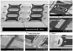
Reprinted with permission from [84].
Copyright 2005 IEEE.
FeaturesSingle Pole, Single Throw Ohmic/capacitive switch
Electromagnetic actuation 4.3 V actuation voltage
Single Pole, 6 Throw Ohmic switch Electrostatic
actuation 27.5 V actuation voltage
GroupChu et al. (2007) [85]Kang et al. (2009) [86]
Image Micromachines 05 00622 i009
Reprinted with permission from [85].
Copyright 2007 IOP Publishing.
Micromachines 05 00622 i010
Reprinted with permission from [86].
Copyright 2009 IOP Publishing.
FeaturesSingle Pole, Double Throw Ohmic switch
Electrostatic actuation 10.2 V actuation voltage
Single Pole, 4 Throw Ohmic switch Electrostatic
actuation15 V actuation voltage
The summary table highlights the trends in the design and specifications for MEMS switches with different electrical and mechanical characteristics. The evolution of the devices from simple switch configurations and actuation mechanisms into more complex and diverse architectures is evident, and it reflects the improvements in design and manufacturing achieved in recent years. Electromagnetic [78,83], electrothermal [80] and piezoelectric [82] devices offer low actuation voltages, albeit requiring constant power [78,80] or the use of permanent magnets [83] to maintain the ON state, or present significant manufacturing challenges [82]. Electrostatic devices, on the contrary, can be produced with simpler manufacturing processes, but require higher actuation voltages. However, the example devices reported in Table 2 show that research is aimed at improving the electrical requirements for electrostatic MEMS switches, with actuation voltages scaling from approximately 30–50 V [77,79,81,84] to 10–15 V [85,86]. Further design and fabrication enhancements have enabled the production of electrostatic MEMS switches with actuation voltages lower than 10 V [21,45,46,47].
Despite the tremendous advances in the performance of electrostatic MEMS switches, electromagnetic devices [78,83] can achieve actuation with lower voltages without the need for particular design improvements. Section 3 details the specific advantages and drawbacks of magnetic MEMS switches compared to electrostatic architectures.

3. Magnetic MEMS Relays

The fabrication of magnetic MEMS requires the same manufacturing techniques typically employed in the production of conventional microelectromechanical devices, with additional challenges associated with the deposition and patterning of soft magnetic materials [87,88,89]. Magnetic actuation requires the magnetisation of movable structures, which are then attracted to the magnetising source or to other external bias field sources. It is important to be able to control and monitor the properties of micromachined magnetic materials [90,91,92,93,94] in order to ensure that the designed structures enter the desired magnetic states during the switch operation (e.g., magnetisation/demagnetisation to temporarily exert an actuation force, or magnetisation in opposite directions under a constant bias field to switch between attraction and repulsion). Section 4 illustrates a series of MEMS devices with different magnetic configurations.
The development of magnetic MEMS devices has generated significant interest as a key-enabler for new applications or for major improvements to existing ones.

3.1. Advantages of Magnetic Actuation

Magnetic MEMS are based on the interaction between sources of electromagnetic or magnetic forces such as coils or permanent magnets and microstructures fabricated with magnetic materials. The strong interest in the application of such old and well-established physics to microscale components lies in the advantages offered by magnetic forces over conventional electrostatic components at smaller scales. As detailed in [7], MEMS employing magnetic actuation potentially offer better performance with respect to other schemes, namely the generation of much higher magnitude forces with lower spatial decay.
A useful figure of merit for actuators is the density of energy U that can be stored in the gaps between the actuating and actuated elements. This metric can be used to calculate approximate values of the pulling forces exerted on the moving part by applying:
Micromachines 05 00622 i011
to the simplified case of scalar quantities.
Referring to the simple calculations proposed by Judy [95], it is possible to make a quick comparison between the energy density capabilities of electrostatic and magnetostatic architectures. The electrostatic energy density in a region of the space where an electric field Micromachines 05 00622 i012 is present can be written as:
Micromachines 05 00622 i013
where ε is the absolute permittivity of the medium and E2 is the square modulus of the electric field Micromachines 05 00622 i012 is.
The value of the electrostatic energy density Uelectrostatic is limited by the maximum electric field and therefore the maximum voltage that can be applied across the designed gap before electrostatic breakdown occurs. This limit field depends on the media between the electrodes and, in terms of voltage, on the distance between the electrodes, as illustrated by the Paschen curve [96] in Figure 3.
Figure 3. Paschen curve: electrostatic breakdown voltage as a function of separation and pressure [95]. Reprinted with permission from [95]. Copyright 2001 IOP Publishing.
Micromachines 05 00622 g003
It is known that devices with very small electrode spacing depart from the behaviour predicted by Paschen’s law [97], and systematic studies of the electrical breakdown have been published for applications of interest for MEMS [98]. A typical limit field value of 3 MV·m−1 yields an energy density in vacuum of the order of 40 J·m−3 [7,95]. It is then possible to perform a similar calculation for the case of magnetostatic actuators. In this case the energy density Umagnetostatic of a region of the space where a magnetic flux density Micromachines 05 00622 i014 is present can be written as:
Micromachines 05 00622 i015
where µ is the permeability of the medium and B2 is the square modulus of the magnetic flux density Micromachines 05 00622 i014. The value of the magnetostatic energy density Umagnetostatic is limited by the saturation flux density, Bsat, of a magnetic material or by the maximum magnetic flux density generated by an electromagnet. For a system with a mid-range flux density in the order of 0.1 T, the associated magnetostatic energy density is around 4000 J·m−3, using the vacuum permeability value µ0 = 4π × 10−7 V·s·A−1·m−1. It is clear from the ratio of these two values (Umagnetostatic / Uelectrostatic ≈ 102) that magnetostatic architectures have a higher energy capability per unit volume. This result is obtained on quantities that represent energy densities, and are thus to a certain extent independent of the dimensions of the fabricated structures. Figure 4 shows a comparison of the energy densities for electrostatic actuators at different voltages and actuators based on magnetic materials such as iron or nickel as a function of the gap distance [95]. The plot shows that there are indeed crossover points where electrostatic systems have greater energy capacity, but this only occurs for very small distances or very high voltages. Unfortunately, both these conditions do not fall into viable ranges for application in integrated MEMS devices.
Figure 4. Comparison of electrostatic and magnetic energy densities as a function of characteristic gap dimensions for various voltages [95]. The dotted line is derived from the Paschen curve [96]. Reprinted with permission from [95]. Copyright 2001 IOP Publishing.
Micromachines 05 00622 g004

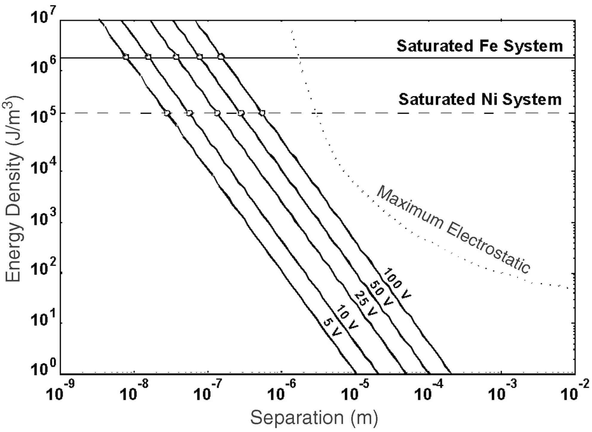
3.2. Excitation Sources

The previous simple arguments favor magnetostatic actuation over electrostatic actuation in terms of the ability to exert intense forces. There are, however, a number of complications associated with magnetic architectures. While electrostatic actuators only require conductive structures and the application of a voltage, magnetic devices must include excitation field sources such as permanent magnets or microcoils. Permanent magnets are great sources of fixed and stable bias fields that can be locally amplified by small patterned structures of soft magnetic material [99]. To achieve a sufficiently uniform bias magnetic flux density over the desired region, however, large permanent magnets are normally required and must be fixed at a sufficiently small distance from the device region to ensure a proper spatial field distribution, as illustrated in Figure 5.
Figure 5. Example of MEMS mounted on permanent magnet assembly, exploded view [100]. Reprinted with permission from [100]. Copyright 2004 IEEE.
Micromachines 05 00622 g005
A number of devices have been reported that employ external permanent magnets to obtain bistable or latching state configurations for magnetic MEMS devices [100,101]. This solution, however, makes it impossible to integrate them into a standard IC process flow and requires additional assembly stages to make the component operational.
Many researchers in the field of magnetic MEMS advocate the use of microformed permanent magnets as integrated components embedded in the microelectromechanical structures as an alternative to externally mounted permanent magnets, and the scaling of permanent magnets to dimensions of the range of interest for microsystems has been documented [102]. A comprehensive work published in 2009 by Arnold reviewed the reported literature on microfabricated permanent magnets [103]. Sputtered [104,105,106], electroplated [91,107,108,109,110] and pulsed-laser [111,112,113] deposited micromagnets have demonstrated excellent magnetic performance at thicknesses up to 100 µm, whereas powder-based fabrication methods facilitate the manufacture of larger structures (up to 1 mm) but with limited properties [114,115,116]. However, the best micromagnets are conventionally deposited rare earth alloys, whose processing unfortunately presents insurmountable challenges that hinder their viability for integration, such as the need for special substrates and high-temperature annealing treatments [103], and exhibit an inconveniently high corrosion rate [117].
The third option involves the patterning of microcoils, a choice that implies an increased level of complication in terms of both design and fabrication and is being actively pursued by many research groups [118,119,120,121]. The magnetic field generation requires an electrical current flow, which has a dramatic impact on the power dissipation and thermal budget characteristics of the manufactured components. Self-heating of the windings poses a reliability issue as the metal tends to expand while embedded in the insulating matrix, e.g., SU-8 [122,123,124] or Parylene [125,126,127]. This can potentially force an uncontrolled stress load on the device. These downsides weigh even more when compared with the freely available field source from the residual magnetisation of a permanent magnet. Even the scaling laws identify permanent magnets as better components for miniaturisation than electromagnets, as illustrated in Figure 6. The same considerations on current densities, heating and scalability led Cugat et al. to the conclusion that micromagnets smaller than 100 µm are difficult to replace with microcoils [128].
However, the fabrication processes required to manufacture microcoils are well established in the industry and readily available within standard silicon cleanrooms, accompanied by significant expertise built over the years on conventional IC and MEMS processing techniques.
Figure 6. Scaling of the current density in a microcoil for equivalence to a 1 T permanent magnet of the same size [128]. Reprinted with permission from [128]. Copyright 2003 IEEE.
Micromachines 05 00622 g006

4. Examples of Magnetic MEMS Switches Reported in the Literature

Pioneering work on the integration of magnetic microactuators has been published by Ahn et al. [129], demonstrating back in 1993 the functional device shown in Figure 7, which is fully compatible with standard IC processing.
A few years later, in 1997, Judy et al. introduced the concepts of magnetic actuation by means of local magnetic forces generated by microcoils and electrostatic latching mechanisms [130], for which a patent was subsequently granted [131]. Conceptual schemes of potential microdevices are shown in Figure 8.
In the same year Wright et al. demonstrated a large force fully integrated electromagnetic actuator [17] that comprises a cantilever beam and a planar electromagnetic coil fabricated through surface and bulk micromachining.
The following sections review some of the most relevant MEMS switching devices reported in the literature, in chronological order, with a particular focus on relays that employ magnetic actuation.
Figure 7. Concept and fabrication of a fully integrated magnetic microactuator [129]. (a) Concept of meander core and corresponding model; (b) Micrograph of the fabricated microactuator; and (c) Scheme of the microactuator. Reprinted with permission from [129]. Copyright 1993 IEEE.
Micromachines 05 00622 g007
Figure 8. Scheme of potential microactuators employing (a) microfabricated coils for local magnetic actuation and (b) electrostatic clamping for latching the actuated state [130]. Reprinted with permission from [130]. Copyright 1997 IEEE.
Micromachines 05 00622 g008

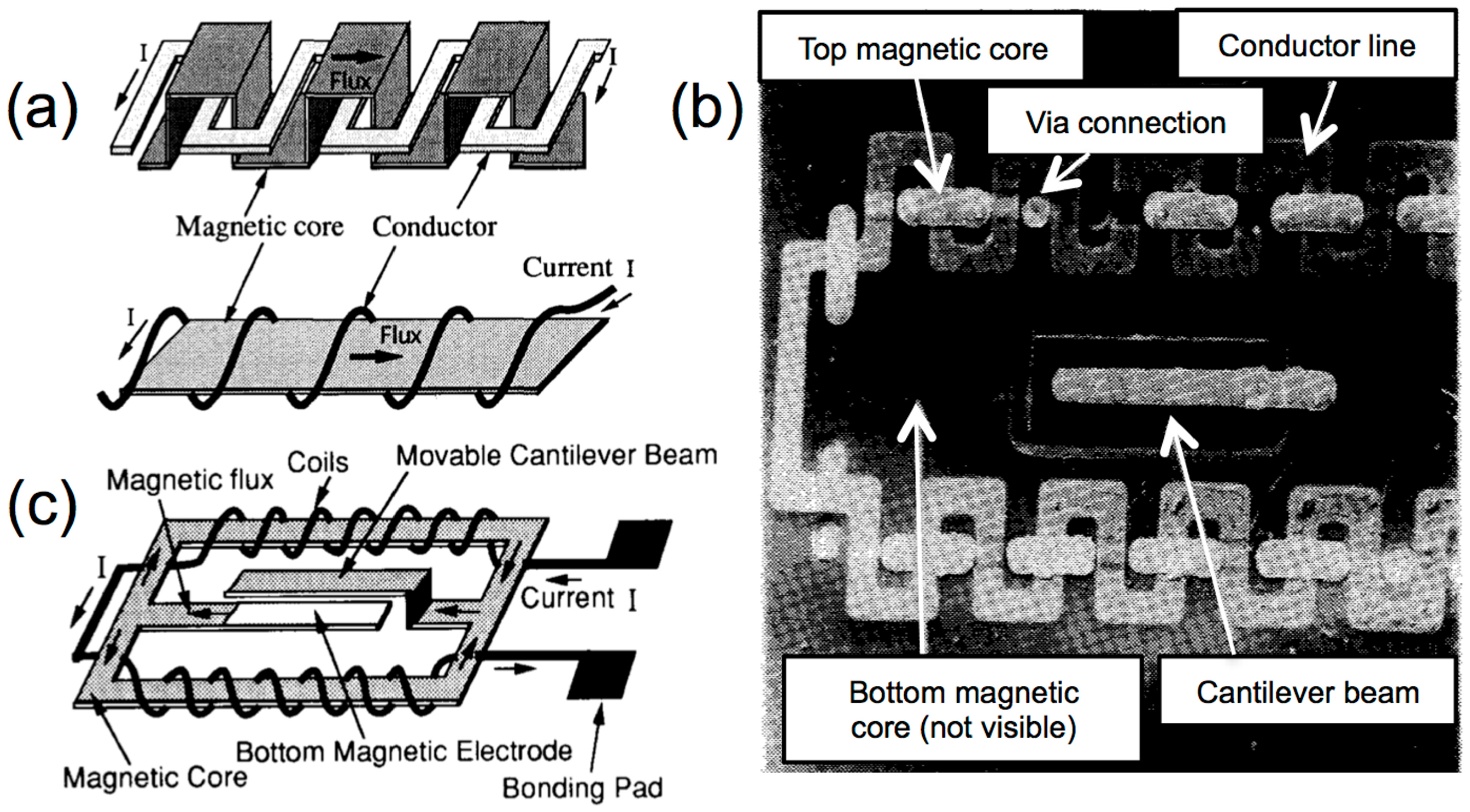
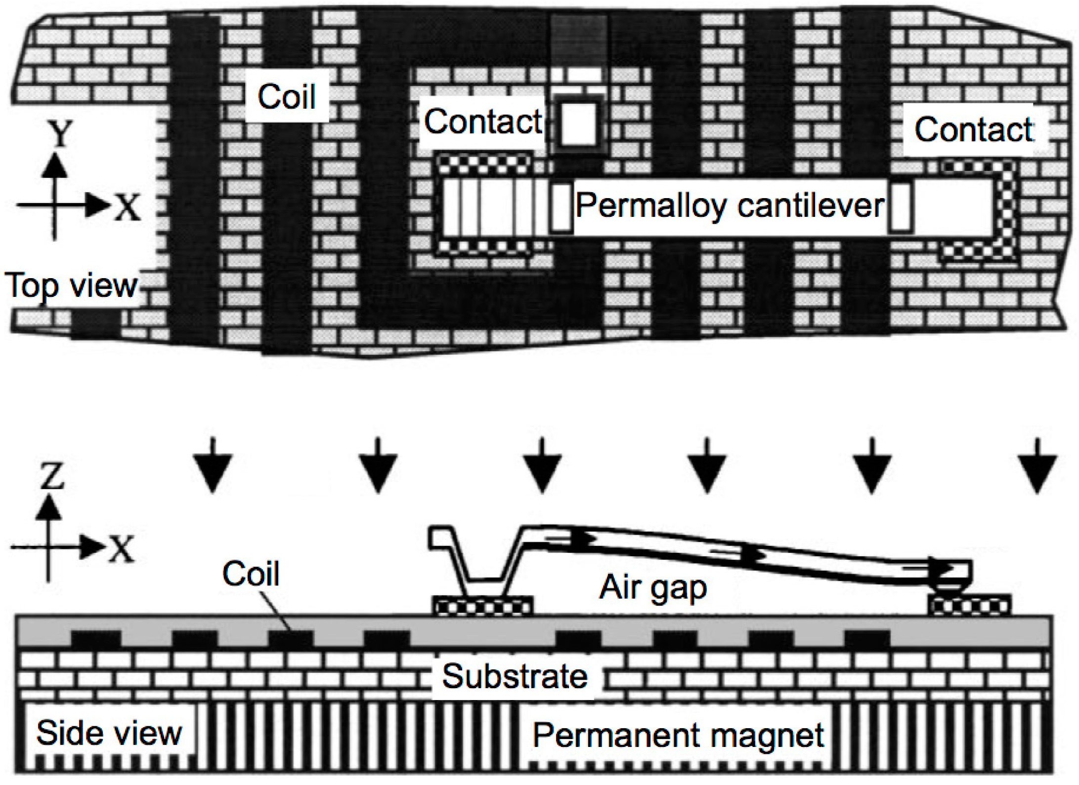
4.1. Taylor et al. (1998) [132]

The first of these devices was reported by Taylor et al. back in 1998 [132], as a follow-up on their previous work [133]. The authors specifically address the incompatibility of previously reported magnetic microrelays for IC integration and propose a device that is fully integrated and comprises a single-layer coil that actuates an upper movable magnetic structure. The production of the device uses low temperature fabrication processes (less than 250 °C) to guarantee compatibility with packaging technologies and to ensure the possibility of manufacturing on substrates already processed with silicon IC. A schematic of the device is presented in Figure 9.
Figure 9. Top view (a) and cross-section (b) of the device presented by Taylor et al. [132]. The magnetic movable plate is attracted to the substrate when a current is passed in the meander coil to generate a magnetic pulling force. Reprinted with permission from [132]. Copyright 1998 IEEE.
Micromachines 05 00622 g009
The fabrication is based on a series of electroplating processes to produce the coils, the bottom and side magnetic cores and the magnetic movable plate. Polyimide is used as a mould for electroplating and as filling material to insulate the coils and the magnetic structures, whereas the movable plate is formed by surface micromachining. The magnetic components are formed with electroplated Ni-Fe. As shown in Figure 9, the relay is normally open and is actuated by flowing an adequate current in the planar coil, which generates a magnetic flux that excites the magnetic structures. A magnetic flux distribution is then formed, subsequently encountering a high reluctance gap between the top surfaces of the core and the bottom surface of the upper plate. A force is exerted on the movable plate, which is attracted to the electromagnet and connects the two ends of the conduction line. Upon removing the excitation current, the elastic restoring forces in the suspension arms bring the structure back to its relaxed position, returning the relay to the OFF state.
The device shows great performance in terms of actuation force, thus resulting in a low contact resistance. The lowest force value of 0.1 mN was achieved at a coil current of 200 mA, allowing for a maximum contact resistance of 38.6 mΩ. The device, however, requires a constant current feed to maintain the ON state, resulting in high power consumption, which rules it out for many applications (e.g., mobile). Additionally the presence of two contacts doubles the probability of failures as outlined in Section 2.2.3.

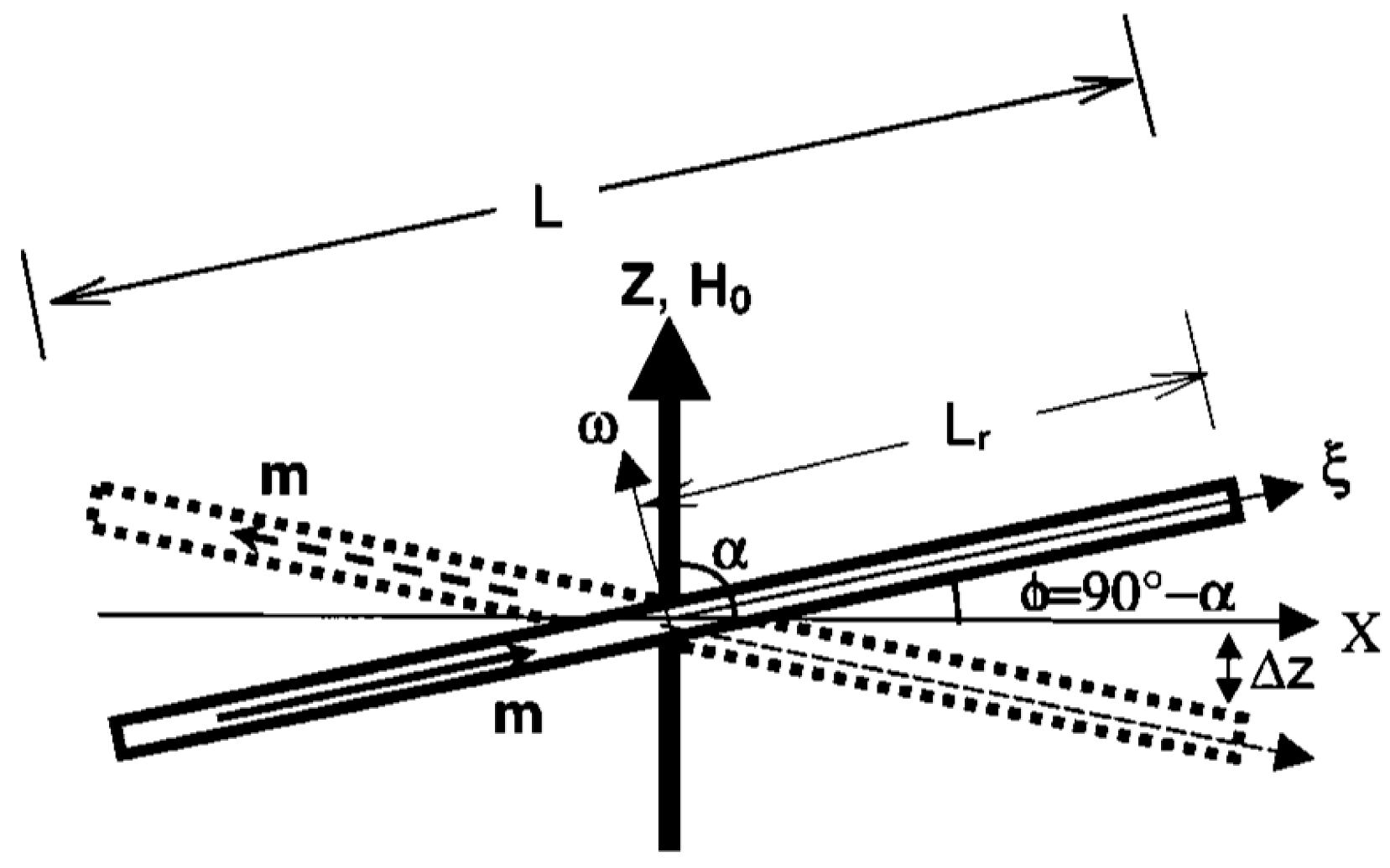
4.2. Ruan et al. (2001) [78,134]

One of the first attempts to produce magnetically actuated microrelay with latching functionality was reported in 2001 by Ruan et al [78,134]. A bistable configuration is achieved by the superimposition of two magnetic effects. A hinged Ni–Fe cantilever is surface micromachined on top of a planar Ag patterned coil, and the whole assembly is then mounted on top of a permanent magnet, as illustrated in Figure 10.
Figure 10. Top view (top) and cross-section (bottom) of the device proposed by Ruan et al. [78]. The device is mounted on a permanent magnet that provides the field needed for the operation. Reprinted with permission from [78], page 347. Copyright 2001 Elsevier.
Micromachines 05 00622 g010
Microcantilevers are highly anisotropic structures that strongly favor magnetization along their easy axis corresponding to their length [10]. A magnetized cantilever in an external bias field experiences a torque that tends to align the magnetization M to the field axis and orientation. The devised architecture utilizes the embedded Ag coil to force the cantilever in one of two possible magnetic states, depending on the polarity of the applied voltage, thus magnetizing the cantilever along its length in either direction. The bias field provided by the permanent magnet then exerts a torque on the hinged cantilever, pulling either of its ends towards the bottom substrate while the other end is pushed upwards. Figure 11 contains a scheme of the geometric configuration of the magnetic vectors. Once the cantilever is forced in a magnetic state, and is consequently aligned to the bias field, the electrical current can be turned off, as the magnetization is then induced solely by the bias field. Mechanical stability can be achieved with the balance between the magnetic torque and the restoring resistance to torsion of the hinges.
Figure 11. Scheme of the magnetic vectors in the device proposed by Ruan et al. [134], where Micromachines 05 00622 i016 is the cantilever magnetisation and Micromachines 05 00622 i017 is the bias magnetic field. Reprinted with permission from [134]. Copyright 2001 IEEE.
Micromachines 05 00622 g011
The bistable latching device offers great performance in terms of power consumption, as only short current pulses are needed to excite the magnetic cantilever. Low contact resistance values are also measured, in the range of 50 to 70 mΩ. On the down side, the device requires assembling onto a permanent magnet, hindering the possible integration in a standard IC process flow, and presents a two-contact architecture, more prone to failures.

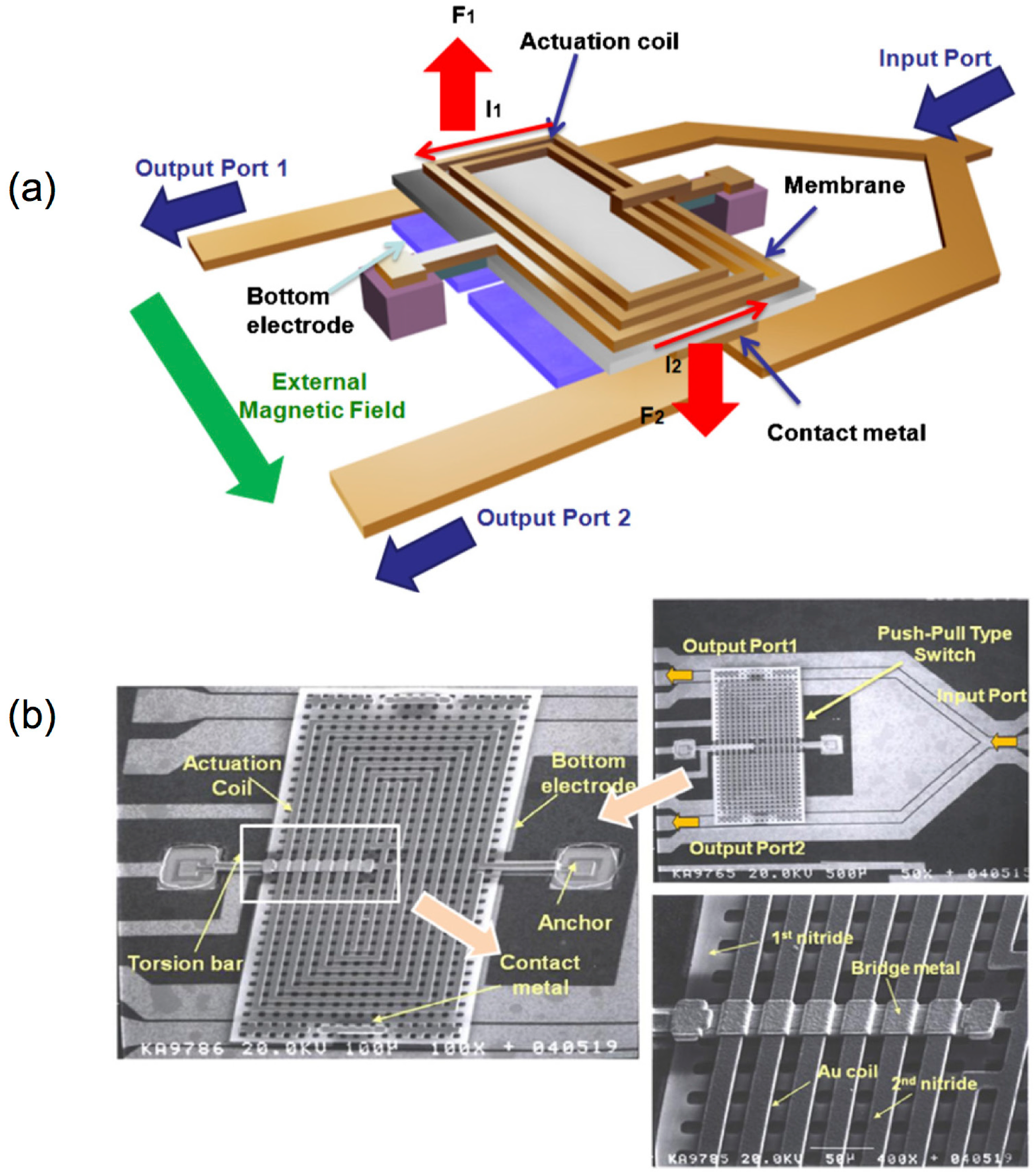
4.3. Cho et al. (2005) [83]

The work reported in 2005 by Cho et al. represents an attempt to integrate electromagnetic and electrostatic actuation mechanisms in a single device, with the aim of providing latching functionality and ensuring low power consumption [83]. The device comprises an insulating movable membrane fabricated as a stack of nitride and a patterned Au microcoil. The structure is then released by surface micromachining, creating a gap between its bottom surface and the substrate. When the device is immersed in a uniform magnetic field such as that provided by a system of external permanent magnets, it is possible to inject a current in the coil to generate a magnetic moment, which experiences magnetic forces that align its orientation to the external field lines. Figure 12 illustrates the architecture of the proposed device.
Figure 12. Diagram (left) and SEM photograph (right) of the ohmic (a) and capacitive (b) devices proposed by Cho et al. [83]. Reprinted with permission from [83]. Copyright 2005 IEEE.
Micromachines 05 00622 g012
Conductive signal lines can be patterned on both surfaces of the membrane so that the actuation can close a contact (ohmic series switch) or vary a capacitance (capacitive shunt switch). Furthermore, two independent conductive plates are patterned on the same surfaces, separated by an insulating layer, to create a parallel plate capacitor with a variable gap. When the suspended membrane is actuated as described above, it approaches the plates and a voltage can then be applied to exert a force between them. If this force is larger than the mechanical restoring force that returns the membrane to the relaxed position, this can act as a latching mechanism that maintains the ON state by simply applying a voltage to charge the capacitor. This is a similar mechanism to that employed in the electrostatic microrelays described in Section 2, with the further advantage of latching the switch in position once the gap is sufficiently reduced by the big initial approach driven by the long-range electromagnetic forces.
The large forces generated by electromagnetic actuation allow for stiffer structures and the use of external permanent magnets as the uniform bias field source allows actuation over very large gaps, as the amplitude of the exerted force in this case does not depend on the distance. This guarantees, in turn, excellent performances in terms of isolation in the OFF state. The experimental data reported in Figure 13 shows that, with minimal actuation current of less than 60 mA, the membrane can be easily displaced for actuation over gaps of big dimensions, following a linear trend.
The electrostatic hold voltage is also very low (<3.7 V) as it intervenes when the gap between the latching capacitor plates is already minimized by the electromagnetic interaction. The energy consumption is calculated to be less than 87.9 µJ per switching cycle. A further advantage of this design is that the transition to the OFF state is aided by passing a current through the actuation coil of the opposite polarity with respect to the ON-state actuation current. The generated magnetic repulsion from the external permanent magnet adds to the mechanical restoring force of the membrane, and helps prevent stiction.
Figure 13. Displacement as function of actuation current in the device proposed by Cho et al. [83]. Reprinted with permission from [83]. Copyright 2005 IEEE.
Micromachines 05 00622 g013

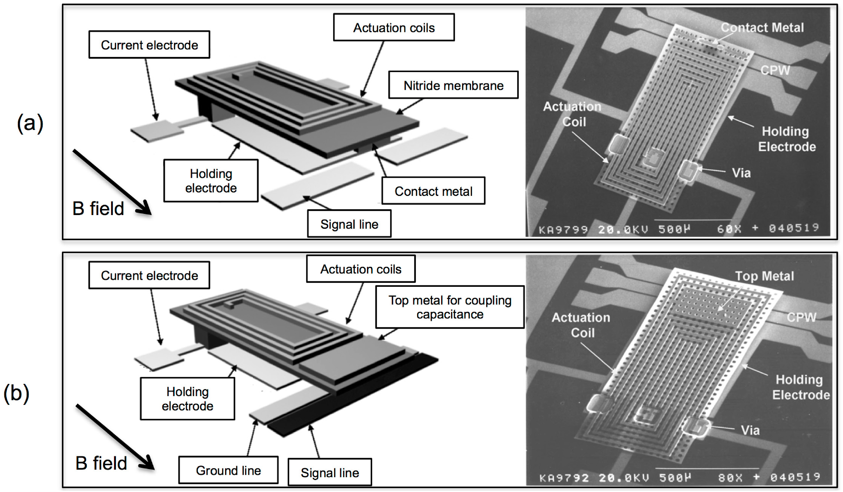
4.4. Cho et al. (2010) [135]

A second latching microrelay was reported by Cho et al. [135] in the form of a single-pole double-throw (SPDT) switch with combined electromagnetic and electrostatic actuation to achieve operation at low power and low voltage. The proposed device is based on the same operation principle previously published by the same group and described in Section 4.3, relying on an external bias field for the creation of stable magnetic states. The same architecture is hence once again used with a different application but no substantial technological modifications. Figure 14 details a diagram and SEM (scanning electron microscope) images of the SPDT device.
A dielectric membrane with integrated coils is hinged and suspended by two dielectric torsion bars that allow its rotation. The electromagnetic forces generated on the coils by a uniform external magnetic field provided by permanent magnets exerts a torque on the membrane system, which rotates and closes one of the two lateral Co-Planar Waveguide (CPW) lines. A pair of patterned bottom electrodes, coupled to the coils on the membrane, serves as electrostatic holding mechanism, activated by applying a voltage when the electromagnetic forces have already closed either of the two CPW contacts. The intense and long-range electromagnetic force guaranteed by the uniform external field enables the design of stiff structures with a record gap of 12.7 μm, for an improved mechanical stability and robustness to vibrations.
Measurements taken on these devices reveal an actuation current of 23 mA and electrostatic hold voltages below 4.3 V, for an energy consumption less than 15.4 μJ per switching cycle. The large gaps result in isolation as high as −54 dB at 2 GHz and −36 dB at 20 GHz and the switch operation has been demonstrated for 166 million actuation cycles. As for its predecessor [83], this device requires external permanent magnets, which hinders IC integration.
Figure 14. Diagram (a) and SEM (scanning electron microscope) images (b) of the SPDT device proposed by Cho et al. [135]. Reprinted with permission from [135]. Copyright 2010 IOP Publishing.
Micromachines 05 00622 g014

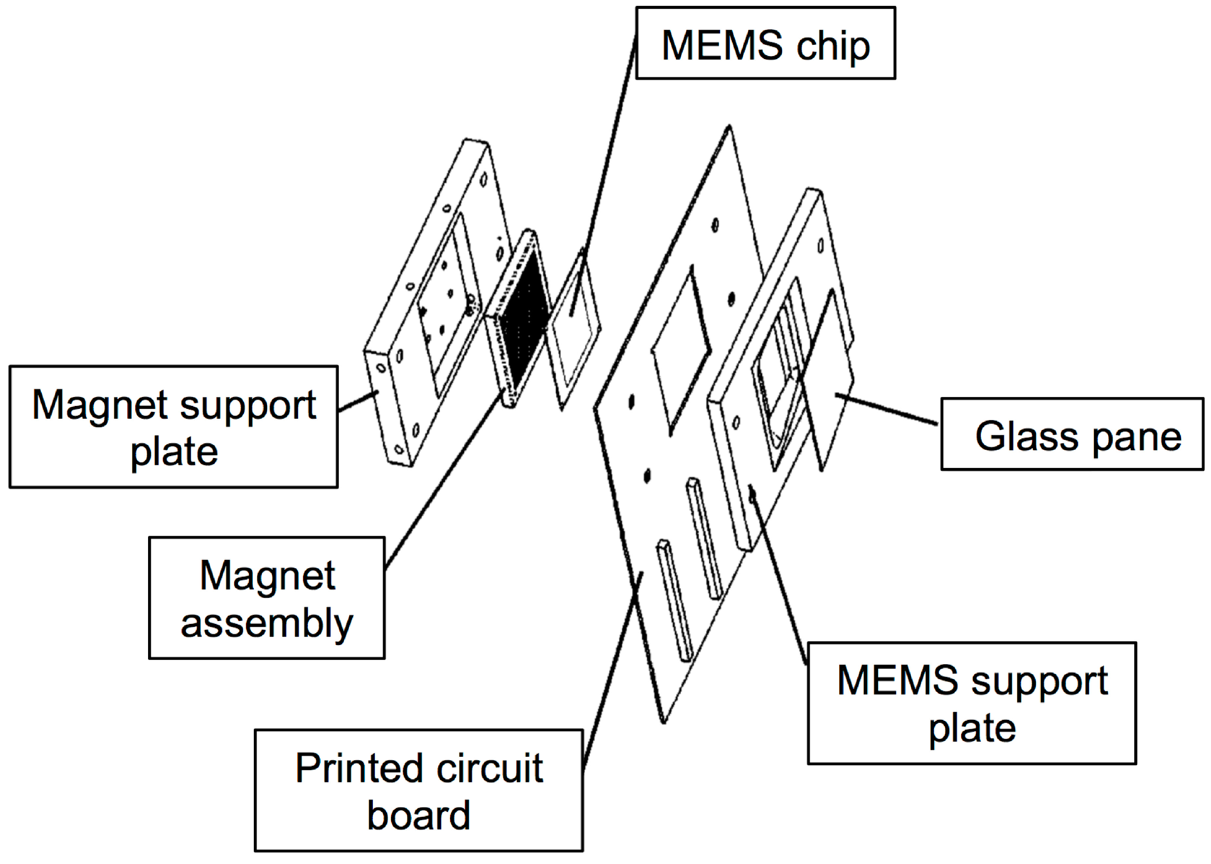
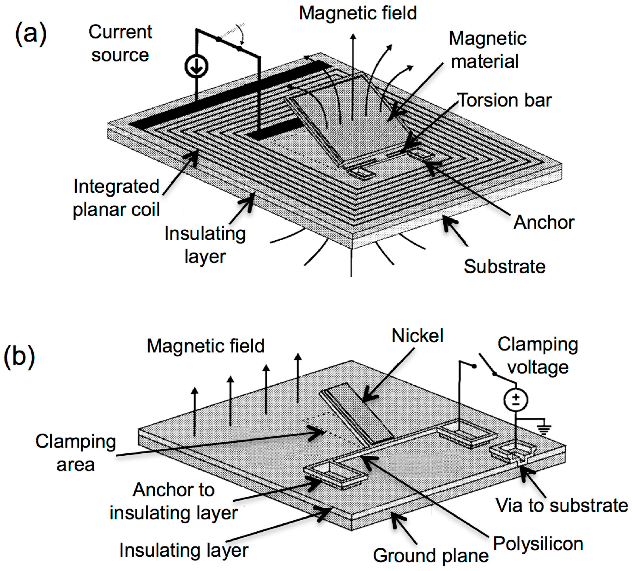
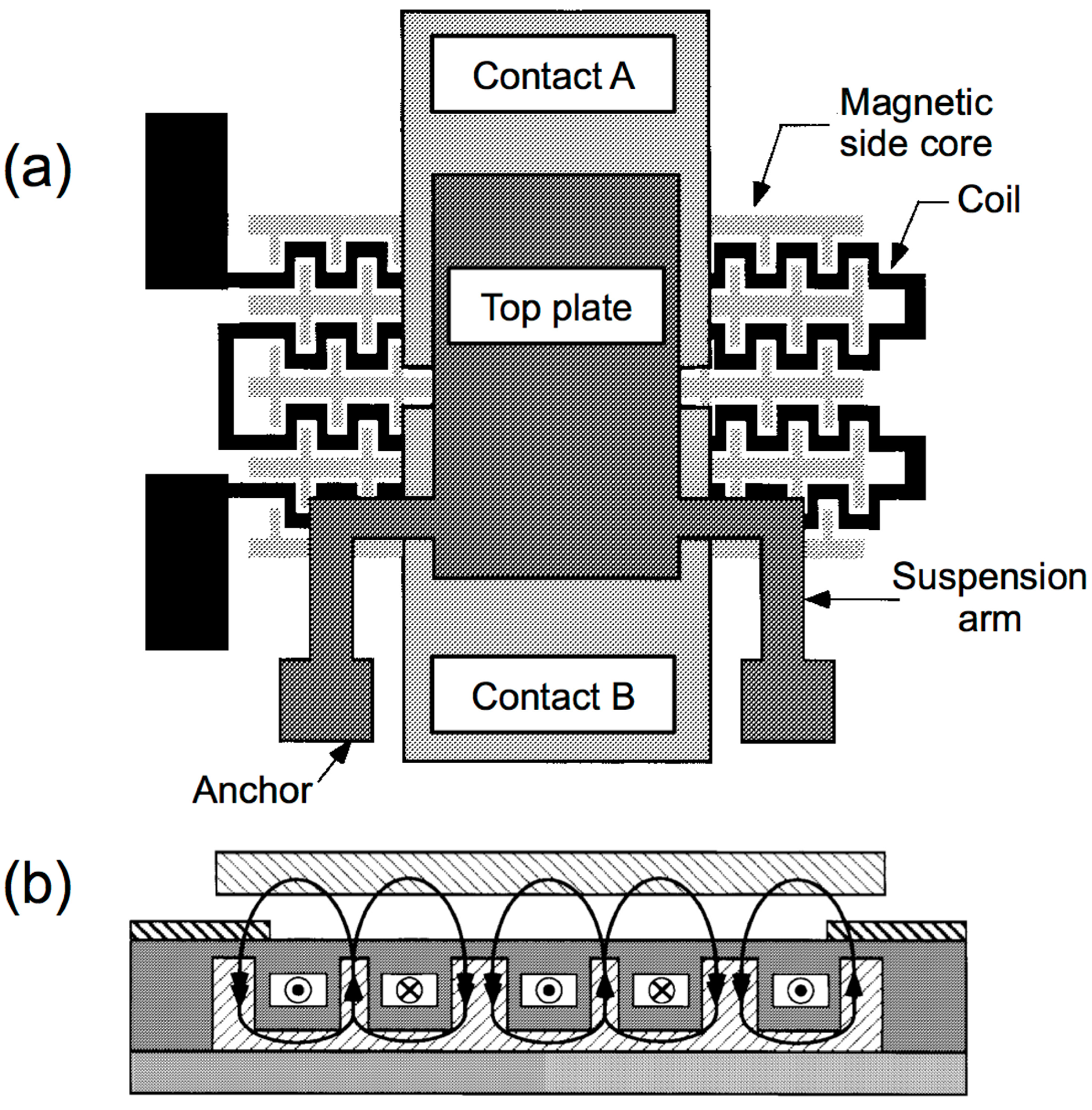
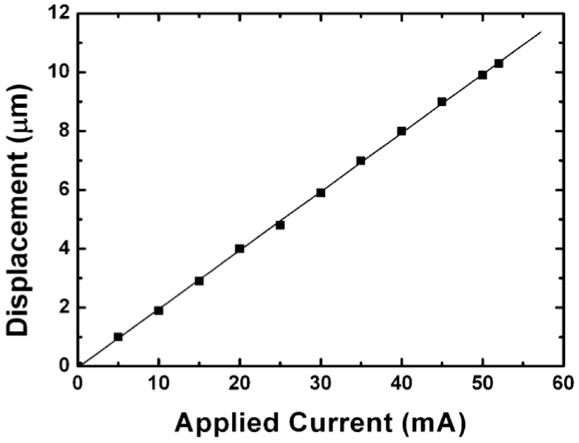
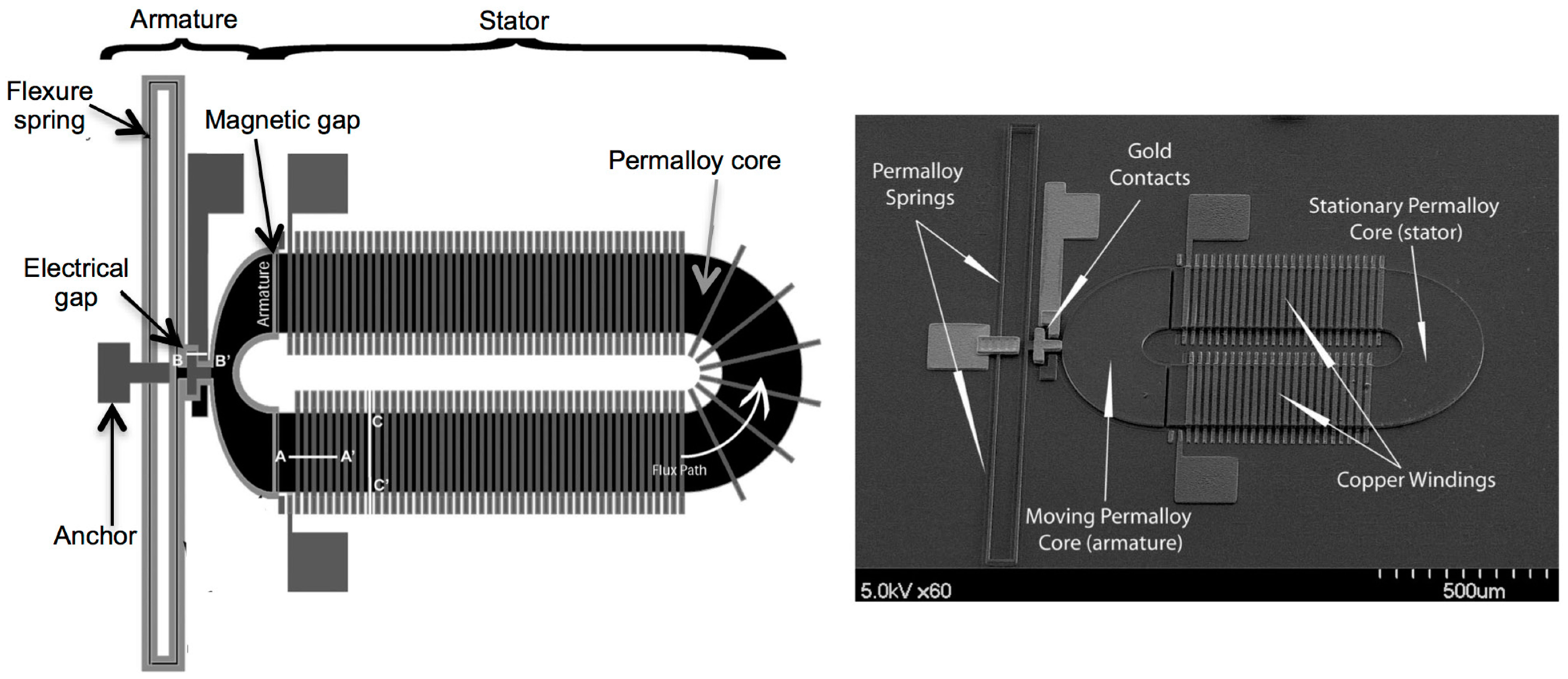
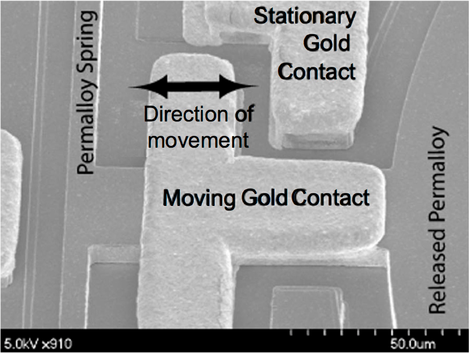
4.5. Glickman et al. [136] (2011)

The authors of this work at UCLA (University of California, Los Angeles) and Shocking Technologies, Inc. focus on the employment of electroplated magnetic films for the fabrication of switching devices. The architecture comprises an actuation section composed of a Ni–Fe horseshoe magnetic core with Cu windings that wrap the entire shape with a 3D geometry based on mesas electroplated below and above the magnetic core, connected together with vias and insulated by a filling polymer. The switching section is designed as a movable magnetic U-shaped pole extension that closes the magnetic loop defined by the actuating section, from which it is separated by an air gap. This structure is suspended on beams and springs and released by the etching of an underlying sacrificial layer to allow horizontal movement. The four-arm architecture with the serpentine design ensures appropriate stiffness and in-plane movement. Figure 15 illustrates the concept drawing and the fabricated device.
The switch contact is designed as a vertical surface contact, as shown in greater detail in Figure 16, that closes with the horizontal movement of the U-shaped pole extension.
Figure 15. Drawing (left) and SEM micrograph (right) of the horseshoe-shaped magnetic switch proposed by Glickman et al. [136]. Reprinted with permission from [136]. Copyright 2011 IEEE.
Micromachines 05 00622 g015
Figure 16. Glickman et al. SEM detail of the switch contact [136]. Reprinted with permission from [136]. Copyright 2011 IEEE.
Micromachines 05 00622 g016
By passing an electrical current into the coil, the Ni–Fe core is excited with a magnetization vector Micromachines 05 00622 i018 that follows the shape of the structure. The magnetic field distribution generated by the magnetized structure in the surrounding space excites in turn the pole extension, which is then attracted to the field source in an attempt to minimize the high reluctance space region of the gap.
A complete actuation model based on reluctance paths is proposed and a comprehensive set of measurements is presented. The prototype does not include any latching mechanism to improve the power consumption characteristics, and the horizontal actuation geometry offers little opportunity for the implementation of conventional mechanisms, unless micromechanical latching is considered with physical hooks and anchors [9,137], which introduce a further manufacturing complication and requires a larger area.

5. Discussion

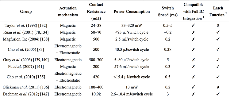
5.1. Summary of the Reviewed Devices: Classification by Smart Power Handling and Full Integrability

The main challenge posed by the manufacturing of magnetic MEMS is the development of efficient and reliable processing techniques to integrate soft magnetic materials within conventionally fabricated electrical and mechanical structures. Table 3 is a summary of some of the features of the magnetic MEMS relays that have been discussed, along with other reported devices. Many publications report RF measurements, namely insertion loss and isolation, on the proposed devices, and these results are not included but can be consulted in the articles referenced in the first column.
It is clear that most of the magnetic MEMS switches reported in the literature employ external permanent magnets to bias the space surrounding the contacts and exert force on the desired components or maintain the actuated state. This is obviously a disadvantage if the switches are to be integrated with Metal-Oxide-Semiconductor (MOS) technology and compatibility with standard IC processing is required. On the other hand, the devices reported in the literature that are IC compatible do not integrate latching mechanisms that enable efficient power management.
Table 3. Magnetic MEMS switches reported in the literature, in chronological order.
GroupActuation mechanismContact Resistance (mΩ)Power ConsumptionSwitch Speed (ms)Compatible with Full IC Integration 1Latch Function 2
Taylor et al. (1998) [132]Magnetic24–3833–320 mW0.5–5
Ruan et al. (2001) [78,134]Magnetic50–70<93 µJ/switch cycle~0.2
Magfusion, Inc (2004) [138]Magnetic5002.5 mJ/switch cycle0.2
Cho et al. (2005) [83]Electromagnetic + Electrostatic50040.3 µJ/switch cycle0.38
Gray et al. (2005) [139,140]Electromagnetic500–7005–80 µJ/switch cycle5
Fu et al. (2007) [141]Magnetic20057.6 mJ/switch cycle0.3
Cho et al. (2010) [135]Electromagnetic + Electrostatic420<15.4 µJ/switch cycle0.5
Glickman et al. (2011) [136]Electromagnetic100–40013 mW0.2
Bachman et al. (2012) [142]Electromagnetic10.9k2.6–10.4 mJ/switch cycle3
Notes: 1 The symbol ✓ indicates that the manufacturing and assembly process for the reported device can be integrated in a standard IC process flow, whereas the symbol ✗ indicates that some of the steps required for production (including assembly with permanent magnets) prevent the integration of the manufacturing process within a standard IC fabrication flow. 2 The symbol ✓ indicates that the reported device incorporates a latching mechanism of some sort that enables the actuated state to be held with no constant power dissipation, whereas the symbol ✗ indicates that the device consumes a constant power to hold the actuated state.

5.2. Performance Trends

It is interesting to compare the performance registered by the devices reported over the past decade, in order to trace the advances achieved by research groups and to identify technological trends. Table 4 provides a list of the performance parameters reported for some of the earlier and latest reviewed devices. Illustrative figures of improvement based on the published results are proposed in the last column.
Table 4. Performance comparison between magnetic MEMS switches reported in the past decade.
Benchmark ParameterValues for Earlier DevicesValues for Recent DevicesAvg. Improvement
Power consumption (non-latching)33 mW [132]13 mW [136]60.6% reduction
Power consumption (latching)93 µJ [78,134]–2.5 mJ [138]5 µJ [140]–15.4 µJ [135]99.21% reduction
Switching speed0.2 ms [138]–0.5 ms [132] 0.2 ms [136]–0.5 ms [135]No improvement
Contact resistance24 mΩ [132]–500 mΩ [138]100 mΩ [136]–420 mΩ [135]No improvement
Lifetime850k cyc. [132]–4.8M cyc. [78] 3M cyc. [136]–100M cyc. [135]16× increase
Device area10 mm2 [134]–25 mm2 [132]0.5 mm2 [135]–2 mm2 [136]92.86% reduction
Contact force25.2 µN [83]–60 µN [132]46.2 µN [135]–200 µN [136]1.89× increase
Max frequency6 GHz [138]3 GHz [140]–20 GHz [135]1.92× increase
Min isolation45 dB [138]36 dB [135]–50 dB [140]No improvement
Max insertion loss0.5 dB [138]0.34 dB [140]–0.52 dB [135]14% reduction
The figures presented in Table 4 reveal considerable improvements when comparing magnetic MEMS switches demonstrated in the late 1990s and early 2000s to devices of the same type reported in recent years. Among the investigated parameters, significant improvements are observed in power dissipation and device area. More advanced latching mechanisms for switching devices, particularly electrostatic hold elements, have in fact enabled a drastic reduction of the energy required to operate switching cycles. The reduction in device area is a commonly observed trend. A more interesting figure of merit would be the ratio between the switched power capability and the device area. Unfortunately, not enough data is presently available for magnetic MEMS relays to enable trends of such quantity to be drawn.
A considerable enhancement is likewise seen in the lifetime of the reported devices, with tremendous improvements demonstrated during reliability testing. This trend is of particular significance, as the device lifetime is a key-enabler for the developed technologies to be transferred to the market, and further increases are crucial for the successful employment of these devices in commercial applications [10].
A more moderate improvement is observed for the RF switch characteristics, namely operational bandwidth, isolation and insertion loss. It is important to note that most of the earliest articles do not report on RF characteristics, but are rather focused on introducing novel architectures, demonstrating manufacturability, and characterizing magnetic actuation mechanisms for MEMS switches. The reporting of RF measurements for magnetic MEMS relays seen in the latest publications is therefore per se an improvement, as the devices are being brought forward, past the fabrication and functionality testing, to the performance characterization stage.
A final observation is dedicated to the generated forces. While there is a trend to increase the contact force to decrease the contact resistance, with a 1.89× average improvement seen for the reviewed devices, it is important to note that some of the presented switches are more prone to stiction in the ON state than others. Specifically, conventional reluctance-based actuators generate magnetic forces that bring together two detached structures. Once the actuation force is removed, the structures return to the previous state subject to mechanical restoring force. This is the case for some of the switches presented in the previous section [129,132,136]. Other devices, instead, use a counter-actuation force that pushes the mechanical structures away from the contact or to another contact depending on the throws of the switch. This is achieved by reversing the magnetisation of an anisotropic structure such as a cantilever [78,134], or by temporarily generating a magnetic field that opposes the polarity of an externally mounted permanent magnet [83,135]. This is a significant advantage in terms of preventing stiction, and may prove beneficial for an enhanced reliability.

5.3. Future Research

The reviewed devices highlight a general trend that sees designers envisaging magnetic MEMS switches with latching mechanisms of different sorts, in order to benefit from a reduction in power requirements [78,83,134,135]. Most of these devices require external permanent magnets to provide the switch space with a bias magnetic field. This prevents the complete integration of the manufacturing process into standard IC fabrication flows as it further introduces the need for additional assembly and packaging operations, with an associated increase in the overall cost.
The switches proposed by Taylor et al. [132] and Glickman et al. [136], instead, offer full compatibility with IC technology, with the drawback of requiring constant power dissipation to maintain the ON state.
Research efforts may therefore be envisaged that aim at bringing together full IC compatibility and latching functionality to prevent constant power consumption. Hybrid electromagnetic and electrostatic MEMS switches can in fact offer fully integrated magnetic actuation capabilities with smart power management by incorporating electrostatic clamps that hold the device in the ON state with very low power consumption.

6. Conclusions

The presented review highlights the advantages and the challenges of magnetic MEMS switches. A key objective for the successful transfer to the market of magnetic MEMS technologies is the development of architectures that offer the high OFF-state isolation at RF frequency and the robustness to wear and failure that are typical of magnetic actuation, with the added benefits of full IC compatibility and smart power management.
Future research should clearly be focused on developing the technologies to enable the production of fully integrated magnetic MEMS relays that combine electromagnetic actuation and electrostatic or mechanical mechanisms that hold the switch state at near-zero power consumption, in order to achieve switching at very low power and with high isolation in high frequency applications. Successful architectures will have a high commercial potential in the market of electronic components, particularly for high frequency applications, where MEMS switches offer significant advantages compared to solid state devices in terms of high OFF-state isolation and low power consumption, with typical applications being cellular signal transmission, airborne communication systems, phased arrays, and so on.

Acknowledgments

The authors would like to acknowledge the financial support of the Edinburgh Research Partnership in Engineering and Mathematics, and of the Engineering and Physical Sciences Research Council (EPSRC)/Innovative Electronics Manufacture Research Centre (IeMRC) through Doctoral Training Award (DTA) funding DTA/15/2007, IeMRC/EPSRC (FS/01/02/10), and the latter through the grant entitled “Smart Microsystems”. Further financial support during the writing of the article was made possible through the EPSRC grant entitled “USINN” and referenced EP/K020250/1.

Author Contributions

Giuseppe Schiavone reviewed the work published in the literature and drew global research trends in integrated magnetic MEMS switches. He compared relevant devices reported by research groups in recent years and identified the benefits and drawbacks of each. Anthony J. Walton and Marc P. Y. Desmulliez provided their extensive expertise in reviewing the paper.

Conflicts of Interest

The authors declare no conflict of interest.

References

  1. Ko, W.H. Trends and frontiers of MEMS. Sens. Actuators A Phys. 2007, 136, 62–67. [Google Scholar] [CrossRef]
  2. Wise, K.D. Integrated sensors, MEMS, and microsystems: Reflections on a fantastic voyage. Sens. Actuators A Phys. 2007, 136, 39–50. [Google Scholar] [CrossRef]
  3. Tanaka, M. An industrial and applied review of new MEMS devices features. Microelectron. Eng. 2007, 84, 1341–1344. [Google Scholar]
  4. Bryzek, J. Impact of MEMS technology on society. Sens. Actuators A Phys. 1996, 56, 1–9. [Google Scholar] [CrossRef]
  5. Bao, M.; Wang, W. Future of microelectromechanical systems (MEMS). Sens. Actuators A Phys. 1996, 56, 135–141. [Google Scholar] [CrossRef]
  6. Lang, W. Reflexions on the future of microsystems. Sens. Actuators A Phys. 1999, 72, 1–15. [Google Scholar] [CrossRef]
  7. Niarchos, D. Magnetic MEMS: Key issues and some applications. Sens. Actuators A Phys. 2003, 109, 255–262. [Google Scholar] [CrossRef]
  8. Rebeiz, G.M.; Muldavin, J.B. RF MEMS switches and switch circuits. IEEE Microw. Mag. 2001, 4, 59–71. [Google Scholar]
  9. Choi, J.Y.; Ruan, J.; Coccetti, F.; Lucyszyn, S. Three-dimensional RF MEMS switch for power applications. IEEE Trans. Ind. Electron. 2009, 56, 1031–1039. [Google Scholar] [CrossRef]
  10. Rebeiz, G.M. RF MEMS switches: Status of the technology. In Proceedings of the 12th International Conference on Solid State Sensors, Actuators and Microsystems, Boston, MA, USA, 8–12 June 2003; pp. 1726–1729.
  11. Brown, E.R. RF-MEMS Switches for reconfigurable integrated circuits. IEEE Trans. Microw. Theory Tech. 1998, 46, 1868–1880. [Google Scholar] [CrossRef]
  12. Rebeiz, G.M. RF MEMS—Theory, Design and Technology; John Wiley&Sons, Inc.: Hoboken, NJ, USA, 2003. [Google Scholar]
  13. Li, X.; Lang, L.; Liu, J.; Xia, Y.; Yin, L.; Hu, J.B.; Fang, D.; Zhang, H. Electro-thermally Actuated RF MEMS switch for wireless communication. In Proceedings of the 5th IEEE International Conference on Nano/Micro Engineered and Molecular Systems, Xiamen, China, 20–23 January 2010; pp. 497–500.
  14. Pal, J.; Zhu, Y.; Lu, J.; Dao, D.V.; Khan, F. RF MEMS switches for smart antennas. Microsyst. Technol. 2014, 20, 1–9. [Google Scholar] [CrossRef]
  15. Cho, J.H.; Ahn, C.H. A Bidirectional mmagnetic microactuator using electroplated permanent magnet arrays. IEEE J. Microelectromech. Syst. 2002, 11, 78–84. [Google Scholar]
  16. Getpreecharsawas, J.; Puchades, I.; Hournbuckle, B.; Fuller, L.; Pearson, R.; Lyshevski, S. An electromagnetic MEMS actuator for micropumps. In Proceedings of the 2nd International Conference on Perspective Technologies and Methods in MEMS Design, Lviv, Ukraine, 24–27 May 2006; pp. 11–14.
  17. Wright, J.A.; Tai, Y.C.; Chang, S.C. A large-force, fully-integrated MEMS magnetic actuator. In Proceedings of the International Conference on Solid State Sensors and Actuators, TRANSDUCERS’97, Chicago, IL, USA, 16–19 June 1997; pp. 793–796.
  18. Robert, P.; Saias, D.; Billard, C.; Boret, S.; Sillon, N.; Maeder-Pachurka, C.; Charvet, P.L.; Bouche, G.; Ancey, P.; Berruyer, P. Integrated RF-MEMS switch based on a combination of thermal and electrostatic actuation. In Proceedings of the 12th IEEE International Conference on Solid State Sensors, Actuators and Microsystems, Boston, MA, USA, 8–12 June 2003; pp. 1714–1717.
  19. Qiu, J.; Lang, J.H.; Slocum, A.H.; Strümpler, R. A high-current electrothermal bistable MEMS relay. In Proceedings of the IEEE Sixteenth Annual International Conference on Micro Electro Mechanical Systems, Kyoto, Japan, 19–23 January 2003; pp. 64–67.
  20. Daneshmand, M.; Fouladi, S.; Mansour, R.R.; Lisi, M.; Stajcer, T. Thermally actuated latching RF MEMS switch and its characteristics. IEEE Trans. Microw. Theory Tech. 2009, 57, 3229–3238. [Google Scholar] [CrossRef]
  21. Touati, S.; Lorphelin, N.; Kanciurzewski, A.; Robin, R.; Rollier, A.; Mille, O.; Segueni, K. Low actuation voltage totally free flexible RF MEMS switch with antistiction system. In Proceedings of the Symposium on Design, Test, Integration and Packaging of MEMS/MOEMS, Nice, France, 9–11 April 2008; pp. 67–70.
  22. Kaynak, M.; Wietstruck, M.; Scholz, R.; Drews, J.; Barth, R.; Ehwald, K.E.; Fox, A.; Haak, U.; Knoll, D.; Korndorfer, F.; et al. BiCMOS embedded RF-MEMS switch for above 90 GHz applications using backside integration technique. In Proceedings of the 2010 International Electron Devices Meeting (IEDM), San Francisco, CA, USA, 6–8 December 2010; pp. 36.5.1–36.5.4.
  23. Goggin, R.; Wong, J.E.; Hecht, B.; Fitzgerald, P.; Schirmer, M. Fully integrated, high yielding, high reliability DC contact MEMS switch technology&control IC in standard plastic packages. In Proceedings of the IEEE Conference on Sensors, Limerick, Ireland, 28–31 October 2011; pp. 958–961.
  24. Maciel, J.; Majumder, S.; Lampen, J.; Guthy, C. Rugged and reliable ohmic MEMS switches. In Proceedings of the IEEE MTT-S International Microwave Symposium Digest (MTT), Montreal, Canada, 17–22 June 2012; pp. 1–3.
  25. Patel, C.D.; Rebeiz, G.M. A high-reliability high-linearity high-power RF MEMS metal-contact switch for DC-40-GHz applications. IEEE Trans. Microw. Theory Tech. 2012, 60, 3096–3112. [Google Scholar] [CrossRef]
  26. Wang, L.F.; Han, L.; Tang, J.Y.; Huang, Q.A. Lateral contact three-state RF MEMS switch for ground wireless communication by actuating rhombic structures. IEEE J. Microelectromech. Syst. 2013, 22, 10–12. [Google Scholar] [CrossRef]
  27. Cohn, M.B.; Saechao, K.; Whitlock, M.; Brenman, D.; Tang, W.T.; Proie, R.M. RF MEMS switches for wide I/O data bus applications. In Proceedings of the IEEE International Test Conference (ITC), Anaheim, CA, USA, 6–13 September 2013; pp. 1–8.
  28. Hwang, J.; Hwang, S.H.; Lee, Y.S.; Kim, Y.K. A low-loss RF MEMS silicon switch using reflowed glass structure. In Proceedings of the IEEE 27th International Conference on Micro Electro Mechanical Systems (MEMS), San Francisco, CA, USA, 26–30 January 2014; pp. 1233–1236.
  29. Koul, S.K.; Dey, S. RF MEMS true-time-delay phase shifter. In Micro and Smart Devices and Systems; Springer (India) Private Ltd.: New Dehli, India, 2014; pp. 467–485. [Google Scholar]
  30. Angira, M.; Rangra, K. Design and investigation of a low insertion loss, broadband, enhanced self and hold down power RF-MEMS switch. Microsyst. Technol. 2014, 20, 1–6. [Google Scholar] [CrossRef]
  31. Seki, T.; Yamamoto, J.; Murakami, A.; Yoshitake, N.; Hinuma, K.I.; Fujiwara, T.; Sano, K.; Matsushita, T.; Sato, F.; Oba, M. An RF MEMS switch for 4G Front-Ends. In Proceedings of the IEEE MTT-S International Microwave Symposium Digest (IMS), Seattle, WA, USA, 2–7 June 2013; pp. 1–3.
  32. Luo, X.; Ning, Y.; Molinero, D.; Palego, C.; Hwang, J.C.M.; Goldsmith, C.L. Intermodulation distortion of actuated MEMS capacitive switches. In Proceedings of the IEEE Microwave Measurement Conference (ARFTG), Seattle, WA, USA, 7 June 2013; pp. 1–3.
  33. Dey, S.; Koul, S.K. Design and development of miniaturized high isolation MEMS SPDT switch for Ku-band T/R module application. In Proceedings of the IEEE MTT-S International Microwave and RF Conference, New Delhi, India, 14–16 December 2013; pp. 1–4.
  34. Verger, A.; Pothie, A.; Guines, C.; Blondy, P.; Vendier, O.; Courtade, F. Nanogap MEMS micro-relay with 70 ns switching speed. In Proceedings of the 25th IEEE International Conference on Micro Electro Mechanical Systems (MEMS), Paris, France, 29 January–2 February 2012; pp. 717–720.
  35. Chakraborty, A.; Kundu, A.; Dhar, S.; Maity, S.; Chatterjee, S.; Gupta, B. Compact K-band distributed RF MEMS phase shifter based on high-speed switched capacitors. In Proceedings of the 11th Mediterranean Microwave Symposium (MMS), Hammamet, Tunisia, 8–10 September 2011; pp. 25–28.
  36. Proie, R.M.; Polcawich, R.G.; Pulskamp, J.S.; Ivanov, T.; Zaghloul, M.E. Development of a PZT MEMS switch architecture for low-power digital applications. IEEE J. Microelectromech. Syst. 2011, 20, 1032–1042. [Google Scholar]
  37. Tabib-Azar, M.; Venumbaka, S.R.; Alzoubi, K.; Saab, D. 1 Volt, 1 GHz NEMS switches. In Proceedings of the IEEE Sensors Conference, Kona, HI, USA, 1–4 November 2010; pp. 1424–1426.
  38. Yamane, D.; Sun, W.; Seita, H.; Kawasaki, S.; Fujita, H.; Toshiyoshi, H. An SOI bulk-micromachined dual SPDT RF-MEMS switch by layer-wise separation design of waveguide and switching mechanism. IEICE Electron. Express 2010, 7, 80–85. [Google Scholar] [CrossRef]
  39. Chan, K.; Ramer, R. A novel RF MEMS switch with novel mechanical structure modeling. J. Micromech. Microeng. 2010, 20. [Google Scholar] [CrossRef]
  40. Van Spengen, W.M.; Puers, R.; Martens, R.; de Wolf, I. A comprehensive model to predict the charging and reliability of capacitive RF MEMS switches. J. Micromech. Microeng. 2004, 14, 514–521. [Google Scholar] [CrossRef]
  41. Blondy, P.; Crunteanu, A.; Champeaux, C.; Catherinot, A.; Tristant, P.; Vendier, O.; Cazaux, J.L.; Marchand, L. Dielectric less capacitive MEMS switches. In Proceedings of the IEEE MTT-S International Microwave Symposium Digest, Fort Worth, TX, USA, 6–11 June 2004; pp. 573–576.
  42. Massenz, A.; Barbato, M.; Giliberto, V.; Margesin, B.; Colpo, S.; Meneghesso, G. Investigation methods and approaches for alleviating charge trapping phenomena in ohmic RF-MEMS switches submitted to cycling test. Microelectron. Reliab. 2011, 51, 1887–1891. [Google Scholar] [CrossRef]
  43. Li, G.; Zhang, W.; Li, P.; Sang, S.; Hu, J.; Chen, X. Investigation of charge injection and relaxation in multilayer dielectric stacks for capacitive RF MEMS switch application. IEEE Trans. Electron Devices 2013, 60, 2379–2387. [Google Scholar] [CrossRef]
  44. Chu, C.; Shih, W.; Chung, S.; Tsai, H.; Chang, T.S.P. A low actuation voltage electrostatic actuator for RF MEMS switch applications. J. Micromech. Microeng. 2007, 17, 1649–1656. [Google Scholar]
  45. Pacheco, S.P.; Katehi, L.P.B.; Nguyen, C.T.C. Design of low actuation voltage RF MEMS switch. In Proceedings of International Microwave Symposium Digest, Boston, MA, USA, 11–16 June 2000; pp. 165–168.
  46. Robin, R.; Touati, S.; Segueni, K.; Millet, O.; Buchaillot, L. A new four states high deflection low actuation voltage electrostatic MEMS switch for RF applications. In Proceedings of the Symposium on Design, Test, Integration and Packaging of MEMS/MOEMS, Nice, France, 9–11 April 2008; pp. 56–59.
  47. Hah, D.; Yoon, E.; Hong, S. A low-voltage actuated micromachined microwave switch using torsion springs and leverage. IEEE Trans. Microw. Theory Tech. 2000, 48, 2540–2545. [Google Scholar]
  48. Bell, D.J.; Lu, T.J.; Fleck, N.A.; Spearing, S.M. MEMS actuators and sensors: observations on their performance and selection for purpose. J. Micromech. Microeng. 2005, 15, S153–S164. [Google Scholar]
  49. Van Spengen, W.M. MEMS reliability from a failure mechanisms perspective. Microelectron. Reliab. 2003, 43, 1049–1060. [Google Scholar]
  50. Vincent, M.; Chiesi, L.; Fourrier, J.; Garnier, A.; Grappe, B.; Lapiere, C.; Coutier, C.; Samperio, A.; Paineau, S.; Houze, F.; Noel, S. Electrical contact reliability in a magnetic MEMS switch. In Proceedings of the 54th IEEE Holm Conference on Electrical Contacts, Orlando, FL, USA, 27–29 October 2008; pp. 145–150.
  51. Lin, T.H.; Paula, S.; Lu, S.; Lu, H. A study on the performance and reliability of magnetostatic actuated RF MEMS switches. Microelectron. Reliab. 2009, 49, 59–65. [Google Scholar]
  52. Persano, A.; Tazzoli, A.; Cola, A.; Siciliano, P.; Meneghesso, G.; Quaranta, F. Reliability enhancement by suitable actuation waveforms for capacitive RF MEMS switches in III–V technology. IEEE J. Microelectromech. Syst. 2012, 21, 414–419. [Google Scholar]
  53. Newman, H.S. RF MEMS switches and applications. In Proceedings of the 40th IEEE Annual International Reliability Physics Symposium, Dallas, TX, USA, 7–11 April 2002; pp. 111–115.
  54. Coutu, R.A.; Kladitis, P.E.; Leedy, K.D.; Crane, R.L. Selecting metal alloy electric contact materials for MEMS switches. J. Micromech. Microeng. 2004, 14, 1157–1164. [Google Scholar]
  55. Coutu, R.A.; Reid, J.R.; Cortez, R.; Strawser, R.E.; Kladitis, P.E. Microswitches with sputtered Au, AuPd, Au-on-AuPt, and AuPtCu alloy electric contacts. IEEE Trans. Compon. Packag. Technol. 2006, 29, 341–349. [Google Scholar]
  56. Kwon, H.; Choi, D.J.; Park, J.H.; Lee, H.C.; Park, Y.H.; Kim, Y.D.; Nam, H.J.; Joo, Y.C.; Bu, J.U. Contact materials and reliability for high power RF-MEMS switches. In Proceedings of the IEEE 20th International Conference on Micro Electro Mechanical Systems, Hyogo, Japan, 21–25 January 2007; pp. 231–234.
  57. Lee, H.; Coutu, R.A.; Mall, S.; Leedy, K.D. Characterization of metal and metal alloy films as contact materials in MEMS switches. J. Micromech. Microeng. 2006, 16, 557–563. [Google Scholar]
  58. Jensen, B.D.; Huang, K.; Chow, L.; Saitou, K.; Volakis, J.L.; Kurabayashi, K. Asperity heating for repair of metal contact RF MEMS switches. In Proceedings of the 2004 IEEE MTT-S International Microwave Symposium Digest, Fort Worth, TX, USA, 6–11 June 2004; pp. 1939–1942.
  59. Goldsmith, C.; Ehmke, J.; Malczewski, A.; Pillans, B.; Eshelman, S.; Yao, Z.; Brank, J.; Eberly, M. Lifetime characterization of capacitive RF MEMS switches. In Proceedings of the 2001 IEEE MTT-S International Microwave Symposium Digest, Phoenix, AZ, USA, 20–24 May 2001; pp. 227–230.
  60. Marcelli, R.; Papaioannu, G.; Catoni, S.; de Angelis, G.; Lucibello, A.; Proietti, E.; Margesin, B.; Giacomozzi, F.; Deborgies, F. Dielectric charging in microwave microelectromechanical ohmic series and capacitive shunt switches. J. Appl. Phys. 2009, 105. [Google Scholar] [CrossRef]
  61. Marcelli, R.; Bartolucci, G.; Papaioannu, G.; de Angelis, G.; Lucibello, A.; Proietti, E.; Margesin, B.; Giacomozzi, F.; Deborgies, F. Reliability of RF MEMS switches due to charging effects and their circuital modelling. Microsyst. Technol. 2010, 16, 1111–1118. [Google Scholar]
  62. Persano, A.; Tazzoli, A.; Farinelli, P.; Meneghesso, G.; Siciliano, P.; Quaranta, F. K-band capacitive MEMS switches on GaAs substrate: Design, fabrication, and reliability. Microelectron. Reliab. 2012, 51, 2245–2249. [Google Scholar]
  63. Kruglick, E.; Pister, K. Lateral MEMS microcontact considerations. IEEE J. Microelectromech. Syst. 1999, 8, 264–271. [Google Scholar]
  64. Iannacci, J.; Faes, A.; Repchankova, A.; Tazzoli, A.; Meneghesso, G. An active heat-based restoring mechanism for improving the reliability of RF-MEMS switches. Microelectron. Reliab. 2011, 51, 1869–1873. [Google Scholar]
  65. Jensen, B.D.; Chow, L.L.W.; Huang, K.; Saitou, K.; Volakis, J.L.; Kurabayashi, K. Effect of nanoscale heating on electrical transport in RF MEMS switch contacts. IEEE J. Microelectromech. Syst. 2005, 14, 935–946. [Google Scholar]
  66. Patton, S.T.; Zabinski, J.S. Fundamental studies of Au contacts in MEMS RF switches. Tribol. Lett. 2005, 18, 215–230. [Google Scholar]
  67. Tazzoli, A.; Meneghesso, G. Acceleration of microwelding on ohmic RF-MEMS switches. IEEE J. Microelectromech. Syst. 2011, 20, 552–554. [Google Scholar]
  68. Lucibello, A.; Marcelli, R.; Proietti, E.; Bartolucci, G.; Mulloni, V.; Margesin, B. Reliability of RF MEMS capacitive and ohmic switches for space redundancy configurations. Microsyst. Technol. 2013, 19, 1–11. [Google Scholar]
  69. Pillans, B.; Coryell, L.; Malczewski, A.; Moody, C.; Morris, F.; Brown, A. Advances in RF MEMS phase shifters from 15 GHz to 35 GHz. In Proceedings of the IEEE MTT-S International Microwave Symposium Digest, Montreal, Canada, 17–22 June 2012; pp. 1–3.
  70. Katsuki, T.; Nakatani, T.; Okuda, H.; Toyoda, O.; Ueda, S.; Nakazawa, F. A highly reliable single-crystal silicon RF-MEMS switch using Au sub-micron particles for wafer level LTCC cap packaging. In Proceedings of the 2nd IEEE CPMT Symposium Japan, Kyoto, Japan, 10–12 December 2012; pp. 1–4.
  71. Tas, N.; Sonnenberg, T.; Jansen, H.; Legtenberg, R.; Elwenspoek, M. Stiction in surface micromachining. J. Micromech. Microeng. 1996, 6, 385–397. [Google Scholar]
  72. Grant, P.; Denhoff, M.; Mansour, R. A comparison between RF MEMS switches and semiconductor switches. In Proceedings of the 2004 International Conference on MEMS, NANO and Smart Systems, Banff, AB, Canada, 25–27 August 2004; pp. 515–521.
  73. Yamagajo, T.; Koga, Y. Frequency reconfigurable antenna with MEMS switches for mobile terminals. In Proceedings of the 2011 IEEE-APS Topical Conference on Antennas and Propagation in Wireless Communications (APWC), Turin, Italy, 12–16 September 2011; pp. 1213–1216.
  74. Mahameed, R.; Rebeiz, G.M. RF MEMS capacitive switches for wide temperature range applications using a standard thin-film process. IEEE Trans. Microw. Theory Tech. 2011, 59, 1746–1752. [Google Scholar]
  75. Yang, H.H.; Yahiaoui, A.; Zareie, H.; Blondy, P.; Rebeiz, G.M. A compact high-isolation DC-50 GHz SP4T RF MEMS switch. In Proceedings of the 2014 IEEE MTT-S International Microwave Symposium (IMS), Tampa, FL, USA, 1–6 June 2014; pp. 1–4.
  76. Yao, J.J. RF MEMS from a device perspective. J. Micromech. Microeng. 2000, 10, R9–R38. [Google Scholar]
  77. Yao, Z.J.; Chen, S.; Eshelman, S.; Denniston, D.; Goldsmith, C. Micromachined low-loss microwave switches. IEEE J. Microelectromech. Syst. 1999, 8, 129–134. [Google Scholar]
  78. Ruan, M.; Shen, J.; Wheeler, C.B. Latching microelectromagnetic relays. Sens. Actuators A Phys. 2001, 91, 346–350. [Google Scholar]
  79. Tan, G.L.; Mihailovich, R.; Hacker, J.B.; DeNatale, J.F.; Rebeiz, G.M. Low-loss 2- and 4-bit TTD MEMS phase shifters based on SP4T switches. IEEE Trans. Microw. Theory Tech. 2003, 51, 297–304. [Google Scholar]
  80. Wang, Y.; Li, Z.; McCormick, D.T.; Tien, N.C. A low-voltage lateral MEMS switch with high RF performance. IEEE J. Microelectromech. Syst. 2004, 13, 902–911. [Google Scholar]
  81. Liu, A.; Palei, W.; Tang, M.; Alphones, A. Single-pole-four-throw switch using high-aspect-ratio lateral switches. Electron. Lett. 2004, 40, 1125–1126. [Google Scholar]
  82. Lee, H.C.; Park, J.Y.; Lee, K.H.; Nam, H.J.; Bu, J.U. Silicon bulk micromachined RF MEMS switches with 3.5 volts operation by using piezoelectric actuator. In Proceedings of the 2004 IEEE MTT-S International Microwave Symposium Digest, Fort Worth, TX, USA, 6–11 June 2004; pp. 585–588.
  83. Cho, I.; Song, T.; Baek, S.H.; Yoon, E. A low-voltage and low-power RF MEMS series and shunt switches actuated by combination of electromagnetic and electrostatic forces. IEEE Trans. Microw. Theory Tech. 2005, 53, 2450–2457. [Google Scholar]
  84. Lee, J.; Je, C.H.; Kang, S.; Choi, C.A. A low-loss single-pole six-throw switch based on compact RF MEMS switches. IEEE Trans. Microw. Theory Tech. 2005, 53, 3335–3344. [Google Scholar]
  85. Kang, S.; Kim, H.C.; Chun, K. A low-loss, single-pole, four-throw RF MEMS switch driven by a double stop comb drive. J. Micromech. Microeng. 2009, 19, 1–10. [Google Scholar]
  86. Kang, S.; Kim, H.C.; Chun, K. A low-loss, single-pole, four-throw RF MEMS switch driven by a double stop comb drive. J. Micromech. Microeng. 2009, 19, 1–10. [Google Scholar]
  87. Luo, J.K.; Pritschow, M.; Flewitt, A.J.; Spearing, S.M.; Fleck, N.A.; Milne, W.I. Effects of process conditions on properties of electroplated Ni thin films for microsystem applications. J. Electrochem. Soc. 2006, 153, D155–D161. [Google Scholar]
  88. Arai, K.I.; Honda, T. Micromagnetic actuators. Robotica 1996, 14, 477–481. [Google Scholar]
  89. Hadian, S.E.; Gabe, D.R. Residual stresses in electrodeposits of nickel and nickel–iron alloys. Surf. Coat. Technol. 1999, 122, 118–135. [Google Scholar]
  90. Mathúna, C.O.; Wang, N.; Kulkarni, S.; Roy, S. Review of integrated magnetics for power supply on chip (PwrSoC). IEEE Trans. Power Electron. 2012, 27, 4799–4816. [Google Scholar]
  91. O’Donnel, T.; Wang, N.N.; Kulkarni, S.; Meere, R.; Rhen, F.M.F.; Roy, S.; Mathúna, C.O. Electrodeposited anisotropic NiFe 45/55 thin films for high-frequency micro-inductor applications. J. Magn. Magn. Mater. 2010, 322, 1690–1693. [Google Scholar]
  92. Koo, B.; Yoo, B. Electrodeposition of low-stress NiFe thin films from a highly acidic electrolyte alloys. Surf. Coat. Technol. 2010, 205, 740–744. [Google Scholar]
  93. Flynn, D.; Desmulliez, M.P.Y. Influence of pulse reverse plating on the properties of Ni–Fe thin films. IEEE Trans. Magn. 2010, 46, 979–985. [Google Scholar]
  94. Schiavone, G.; Desmulliez, M.P.Y.; Smith, S.; Murray, J.; Sirotkin, E.; Terry, J.G.; Mount, A.R.; Walton, A.J. Quantitative wafer mapping of residual stress in electroplated NiFe films using independent strain and Young’s modulus measurements. In Proceedings of the 2012 IEEE International Conference on Microelectronic Test Structures (ICMTS 2012), San Diego, CA, USA, 19–22 March 2012; pp. 105–110.
  95. Judy, J.W. Microelectromechanical systems (MEMS): Fabrication, design and applications. Smart Mater. Struct. 2001, 10, 1115–1134. [Google Scholar]
  96. Paschen, F. Ueber die zum Funkenübergang in Luft, Wasserstoff und Kohlensäure bei verschiedenen Drucken erforderliche Potentialdifferenz. Ann. Phys. 1889, 273, 69–96. (In German) [Google Scholar] [CrossRef]
  97. Meek, J.M.; Craggs, J.D. Electrical Breakdown of Gases; Oxford At The Clarendon Press: Oxford, UK, 1953. [Google Scholar]
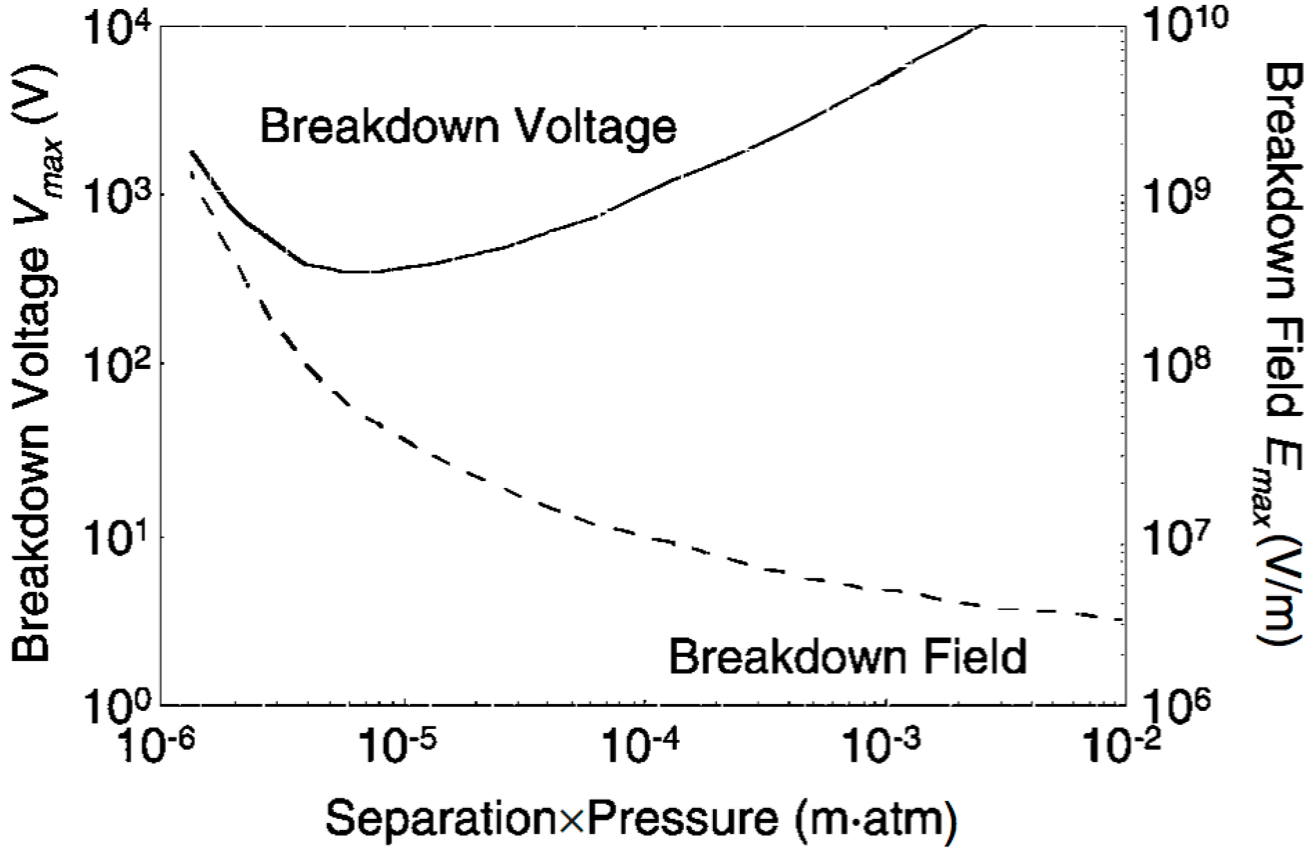
  98. Torres, J.; Dhariwal, R. Electric field breakdown at micrometre separations. Nanotechnology 1999, 10, 102–107. [Google Scholar]
  99. Furlani, E.P. Permanent Magnet and Electromechanical Devices: Materials, Analysis, and Applications (Electromagnetism); Academic Press: Waltham, MA, USA, 2001. [Google Scholar]
  100. Bernstein, J.J.; Taylor, W.P.; Brazzle, J.D.; Corcoran, C.J.; Kirkos, G.; Odhner, J.E.; Pareek, A.; Waelti, M.; Zai, M. Electromagnetically actuated mirror arrays for use in 3-D optical switching applications. IEEE J. Microelectromech. Syst. 2004, 13, 526–535. [Google Scholar]
  101. Blasko, A.S. Integrated Mems Power-Save Switch. U.S. Patent 6,833,597 B2, 21 December 2004. [Google Scholar]
  102. Agashe, J.S.; Arnold, D.P. A study of scaling and geometry effects on the forces between cuboidal and cylindrical magnets using analytical force solutions. J. Phys. D Appl. Phys. 2008, 41. [Google Scholar] [CrossRef]
  103. Arnold, D.P.; Wang, N. Permanent magnets for MEMS. IEEE J. Microelectromech. Syst. 2009, 18, 1255–1266. [Google Scholar]
  104. Pina, E.; Palomares, F.J.; Garcia, M.A.; Cebollada, F.; de Hoyos, A.; Romero, J.J.; Hernando, A.; Gonzalez, J.M. Coercivity in SmCo hard magnetic films for MEMS application. J. Magn. Magn. Mater. 2005, 290, 1234–1236. [Google Scholar]
  105. Budde, T.; Gatzen, H.H. Thin film Sm–Co magnets for use in electromagnetic microactuators. J. Appl. Phys. 2006, 99. [Google Scholar] [CrossRef]
  106. Walther, A.; Givord, D.; Dempsey, N.M.; Khlopkov, K.; Gutfleisch, O. Structural, magnetic, and mechanical properties of 5 μm thick SmCo films suitable for use in microelectromechanical systems. J. Appl. Phys. 2008, 103. [Google Scholar] [CrossRef] [Green Version]
  107. Thongmee, S.; Ding, J.; Lin, J.Y.; Blackwood, D.J.; Yi, J.B.; Yin, J.H. FePt films fabricated by electrodeposition. J. Appl. Phys. 2007, 101. [Google Scholar] [CrossRef]
  108. Wang, N.; Arnold, D.P. Thick electroplated Co-rich Co–Pt micro magnet arrays for magnetic MEMS. IEEE Trans. Magnet. 2008, 44, 3969–3972. [Google Scholar]
  109. Kulkarni, S.; Roy, S. Deposition of thick Co-rich CoPtP films with high energy product for magnetic microelectromechanical applications. J. Magn. Magn. Mater. 2010, 322, 1592–1596. [Google Scholar]
  110. Jamieson, B.; Godsell, J.F.; Wang, N.N.; Roy, S. Device geometry effects in an integrated power microinductor with a Ni45Fe55 enhancement layer. IEEE Trans. Magn. 2013, 49, 869–873. [Google Scholar]
  111. Cadieu, F.J.; Chen, L.; Li, B. Enhanced magnetic properties of nanophase SmCo5 film dispersions. IEEE Trans. Magn. 2001, 37, 2570–2572. [Google Scholar]
  112. Nakano, M.; Sato, S.; Fukunaga, H.; Yamashita, F. A method of preparing anisotropic Nd–Fe–B film magnets by pulsed laser deposition. J. Appl. Phys. 2006, 99. [Google Scholar] [CrossRef]
  113. Nakano, M.; Shibata, S.; Yanai, T.; Fukunaga, H. Anisotropic properties in Fe–Pt thick film magnets. J. Appl. Phys. 2009, 105. [Google Scholar] [CrossRef]
  114. Romero, J.J.; Cuadrado, R.; Pina, E.; do Hoyos, A.; Pigazo, F.; Palomares, F.L.; Hernando, A.; Sastre, R.; Gonzalez, J.M. Anisotropic polymer bonded hard-magnetic films for micro-electromechanical system applications. J. Appl. Phys. 2006, 99. [Google Scholar] [CrossRef]
  115. Bowers, B.J.; Agashe, J.S.; Arnold, D.P. A method to form bonded micromagnets embedded in silicon. In Proceedings of the 14th International Conference on Solid-State Sensors, Actuators and Microsystems (TRANSDUCERS), Lyon, France, 10–14 June 2007; pp. 1581–1584.
  116. Wang, N.; Bowers, B.; Arnold, D.P. Wax-bonded NdFeB micromagnets for microelectromechanical systems application. J. Appl. Phys. 2008, 103. [Google Scholar] [CrossRef]
  117. Chin, T.S. Permanent magnet films for applications in microelectromechanical systems. J. Magn. Magn. Mater. 2000, 209, 75–79. [Google Scholar]
  118. Li, H.Y.; Xie, L.; Ong, L.G.; Baram, A.; Herer, I.; Hirshberg, A.; Chong, S.C.; Kwong, D.L. Ultra-compact micro-coil realized via multilevel dense TSV coil for MEMs application. In Proceedings of the IEEE International 3D System Integration Conference, Osaka, Japan, 31 January–2 February 2012; pp. 1–4.
  119. Kratt, K.; Badilita, V.; Burger, T.; Korvink, J.G.; Wallrabe, U. A fully MEMS-compatible process for 3D high aspect ratio micro coils obtained with an automatic wire bonder. J. Micromech. Microeng. 2010, 20. [Google Scholar] [CrossRef]
  120. Zhao, Y.; Nandra, M.S.; Tai, Y.C. A MEMS intraocular origami coil. In Proceedings of the 16th International Conference on Solid-State Sensors, Actuators and Microsystems (TRANSDUCERS), Beijing, China, 5–9 June 2011; pp. 2172–2175.
  121. Zhao, Y.; Nandra, M.S.; Yu, C.; Tai, Y.C. Reduction of AC resistance in MEMS intraocular foil coils using microfabricated planar Litz structure. In Proceedings of the 7th IEEE International Conference on Nano/Micro Engineered and Molecular Systems (NEMS), Kyoto, Japan, 5–8 March 2012; pp. 234–237.
  122. Grusche, O.G.; Clad, L.; Baxan, N.; Kratt, K.; Mohmmadzadeh, M.; von Elverfeldt, D.; Peter, A.; Hennig, J.; Badilita, V.; Wallrabe, U.; Korvink, J.G. Multilayer phased microcoil array for magnetic resonance imaging. In Proceedings of the 16th International Conference on Solid-State Sensors, Actuators and Microsystems (TRANSDUCERS), Beijing, China, 5–9 June 2011; pp. 962–965.
  123. Xue, N.; Chang, S.P.; Lee, J.B. A SU-8-based microfabricated implantable inductively coupled passive RF wireless intraocular pressure sensor. IEEE J. Microelectromech. Syst. 2012, 21, 1338–1346. [Google Scholar]
  124. Cho, S.H.; Xue, N.; Cauller, L.; Rosellini, W.; Lee, J.B. A SU-8-based fully integrated biocompatible inductively powered wireless neurostimulator. IEEE J. Microelectromech. Syst. 2013, 22, 170–176. [Google Scholar]
  125. Sun, X.; Zheng, Y.; Li, Z.; Li, X.; Zhang, H. Stacked flexible parylene-based 3D inductors with Ni80Fe20 core for wireless power transmission system. In Proceedings of the 26th IEEE International Conference on Micro Electro Mechanical Systems (MEMS), Taipei, Taiwan, 20–24 January 2013; pp. 849–852.
  126. Walker, R.; Sirotkin, E.; Schmueser, I.; Terry, J.G.; Smith, S.; Stevenson, J.T.M.; Walton, A.J. Characterisation and integration of Parylene as an insulating structural layer for high aspect ratio electroplated copper coils. In Proceedings of the 2013 IEEE International Conference on Microelectronic Test Structures (ICMTS 2013), Osaka, Japan, 25–28 March 2013; pp. 7–12.
  127. Zheng, Y.; Sun, X.; Li, Z.; Li, X.; Zhang, H. Flexible MEMS inductors based on Parylene-FeNi Compound Substrate for wireless power transmission system. In Proceedings of the 8th IEEE International Conference on Nano/Micro Engineered and Molecular Systems (NEMS), Suzhou, China, 7–10 April 2013; pp. 1002–1005.
  128. Cugat, O.; Delamare, J.; Reyne, G. Magnetic micro-actuators and systems (MAGMAS). IEEE Trans. Magn. 2003, 39, 3607–3612. [Google Scholar]
  129. Ahn, C.H.; Allen, M.G. A fully integrated surface micromachined magnetic microactuator with a multilevel meander magnetic core. IEEE J. Microelectromech. Syst. 1993, 2, 15–22. [Google Scholar]
  130. Judy, J.W.; Muller, R.S. Magnetically actuated, addressable microstructures. IEEE J. Microelectromech. Syst. 1997, 6, 249–256. [Google Scholar]
  131. Judy, J.W.; Muller, R.S. Magnetic Microactuator. U.S. Patent 5,945,898, 31 August 1999. [Google Scholar]
  132. Taylor, W.P.; Brand, O.; Allen, M.G. Fully integrated magnetically actuated micromachined relays. IEEE J. Microelectromech. Syst. 1998, 7, 181–191. [Google Scholar]
  133. Taylor, W.P.; Allen, M.G. Integrated magnetic microrelays: Normally open, normally closed, and multi-pole devices. In Proceedings of the International Conference on Solid State Sensors and Actuators, TRANSDUCERS’97, Chicago, IL, USA, 16–19 June 1997; pp. 1149–1152.
  134. Ruan, M.; Shen, J.; Wheeler, C.B. Latching micromagnetic relays. IEEE J. Microelectromech. Syst. 2001, 10, 511–517. [Google Scholar]
  135. Cho, I.; Yoon, E. Design and fabrication of a single membrane push-pull SPDT RF MEMS switch operated by electromagnetic actuation and electrostatic hold. J. Micromech. Microeng. 2010, 20, 1–7. [Google Scholar]
  136. Glickman, M.; Tseng, P.; Harrison, J.; Niblock, T.; Goldberg, I.B.; Judy, J.W. High-performance lateral-actuating magnetic MEMS switch. IEEE J. Microelectromech. Syst. 2011, 20, 842–851. [Google Scholar]
  137. Lai, C.H.; Wong, W.S.H. Laterally actuated, low voltage, 3-port RF MEMS switch. In Proceedings of the 19th IEEE International Conference on Micro Electro Mechanical Systems, MEMS 2006, Istanbul, Turkey, 22–26 January 2006; pp. 878–881.
  138. Magfusion Inc. A Magnetic MEMS-Based RF Relay; Microwave Journal&Horizon House Publication: Norwood, MA, USA and London, England, UK, 2004. [Google Scholar]
  139. Gray, G.D., Jr.; Kohl, P.A. Magnetically bistable actuator: Part 1. Ultra-low switching energy and modeling. Sens. Actuators A Phys. 2005, 119, 489–501. [Google Scholar] [CrossRef]
  140. Gray, G.D., Jr.; Prophet, E.M.; Zhua, L.; Kohl, P.A. Magnetically bistable actuator: Part 2. Fabrication and performance. Sens. Actuators A Phys. 2005, 119, 502–511. [Google Scholar]
  141. Fu, S.; Ding, G.; Wang, H.; Yang, Z.; Feng, J. Design and fabrication of a magnetic bi-stable electromagnetic MEMS relay. Microelectron. J. 2007, 38, 556–563. [Google Scholar]
  142. Bachman, M.; Zhang, Y.; Wang, M.; Li, G. High-power magnetically actuated microswitches fabricated in laminates. IEEE Electron Device Lett. 2012, 33, 1309–1311. [Google Scholar]

