Article

Optical Spectrum and Electric Field Waveform Dependent Optically-Induced Dielectrophoretic (ODEP) Micro-Manipulation

1
State Key Laboratory of Robotics, Shenyang Institute of Automation, Chinese Academy of Sciences, 114 Nanta Str., Shenhe Dist., Shenyang 110016, China
2
The Graduate University of the Chinese Academy of Sciences, 19A Yuquanlu, Beijing 100049, China
3
Department of Power Mechanical Engineering, National Tsing Hua University, No. 101, Section 2, Kuang-Fu Road, Hsinchu 30013, Taiwan
4
Department of Mechanical and Biomedical Engineering, City University of Hong Kong, Kowloon, Hong Kong Shatin, NT, Hong Kong
*
Author to whom correspondence should be addressed.
Micromachines 2012, 3(2), 492-508; https://doi.org/10.3390/mi3020492
Submission received: 30 March 2012 / Revised: 1 May 2012 / Accepted: 2 May 2012 / Published: 16 May 2012

Abstract

:
In the last seven years, optoelectronic tweezers using optically-induced dielectrophoretic (ODEP) force have been explored experimentally with much success in manipulating micro/nano objects. However, not much has been done in terms of in-depth understanding of the ODEP-based manipulation process or optimizing the input physical parameters to maximize ODEP force. We present our work on analyzing two significant influencing factors in generating ODEP force on a-Si:H based ODEP chips: (1) the waveforms of the AC electric potential across the fluidic medium in an ODEP chip based microfluidic platform; and (2) optical spectrum of the light image projected onto the ODEP chip. Theoretical and simulation results indicate that when square waves are used as the AC electric potential instead of sine waves, ODEP force can double. Moreover, numerical results show that ODEP force increases with increasing optical frequency of the projected light on an ODEP chip following the Fermi-Dirac function, validating that the optically-induced dielectrophoresis force depends strongly on the electron-hole carrier generation phenomena in optoelectronic materials. Qualitative experimental results that validate the numerical results are also presented in this paper.

1. Introduction

Chiou et al. [1] reported a novel manipulation tool in 2005 which they called optoelectronic tweezers (OET), and which combines the advantages of optical tweezers (i.e., laser-based tweezers) [2] and dielectrophoresis (DEP) [3], as well as using ~100,000 times less optical power than laser-based optical tweezers. This considerably reduced the optical power requirement which is a significant advantage in terms of avoiding damage to live cells during bio-manipulation processes [1]. OET devices are based on optically-induced DEP force (ODEP), which is induced by illuminated optical images onto an hydrogenated amorphous silicon (a-Si:H) surface, i.e., the a-Si:H is used as the photoconductive material that converts visible light into a localized conduction area (matching an illuminated optical image) on a substrate’s surface. Such devices have recently been demonstrated to enable massively parallel manipulation, concentration, transportation, and separation of micro/nano entities by the virtual electrodes induced by the incident light with any desired geometric pattern. Examples of ODEP-based applications include manipulation of single cells [1], cell counting and lysis [4], microparticle counting and sorting [5], manipulation of single DNA molecules [6], parallel trapping of single multiwall carbon nanotubes (CNTs) [7], manipulation and patterning of single wall CNTs [8], dynamic manipulation and separation of individual semiconducting and metallic nanowires [9], dynamic patterning of nanoparticles [10], and manipulation and separation of oil-in-water emulsion droplets [11]. Hence, this new micro/nano manipulation and patterning technique holds excellent potential in terms of realizing parallel fabrication of nano-devices, which is our team’s current research interest. In addition, OET devices that generate light-induced AC electroosmosis (ACEO) have been widely used in the manipulation of nanoparticles [12], dynamic control of local chemical concentration in a fluid [13], measurement of molecular diffusion coefficient [14], assembly of 2D colloidal crystals [15], detection of human tumor markers [16], and rapid and selective concentration of microparticles [17]. Furthermore, the separation of micro-particles of different diameters using different light colors, light intensities [18,19], and widths of virtual line electrodes [19] has also been experimentally validated.
We present in this paper a theoretical formulation on the dependence of the magnitude of ODEP force on: (1) the optical spectrum of the projected image on a photoconductive material; and (2) the applied AC bias waveform across the fluidic medium in an ODEP chip. We note that G. B. Lee’s (a co-author of this paper) group has already demonstrated the increase of ODEP force due to different image colors projected onto the surface of an ODEP chip in [18], however only a qualitative explanation was provided in their prior work. To the best of our knowledge, this paper is the first to present a theoretical model with experimental validation of how the ODEP force varies with the variation of optical spectrum of projected images on ODEP chips. In addition, we will also show theoretically and experimentally that the waveform of the applied AC electric field across the fluid in the ODEP chip will affect the ODEP force magnitude, i.e., higher energy waveforms can induce higher ODEP force.

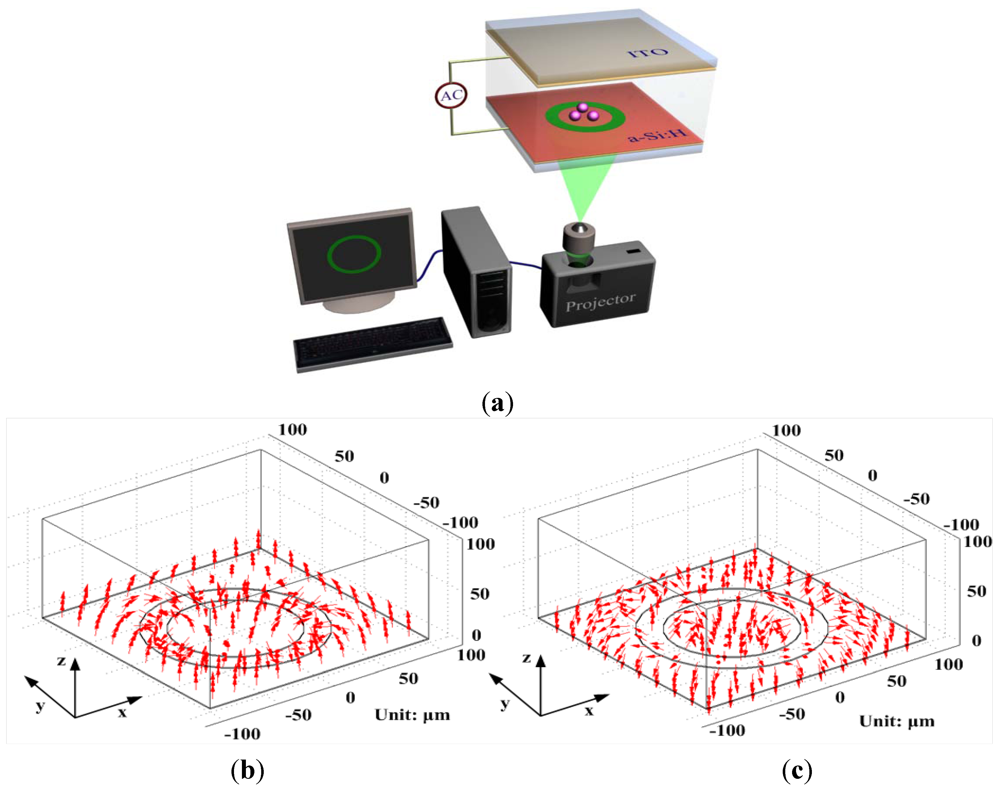
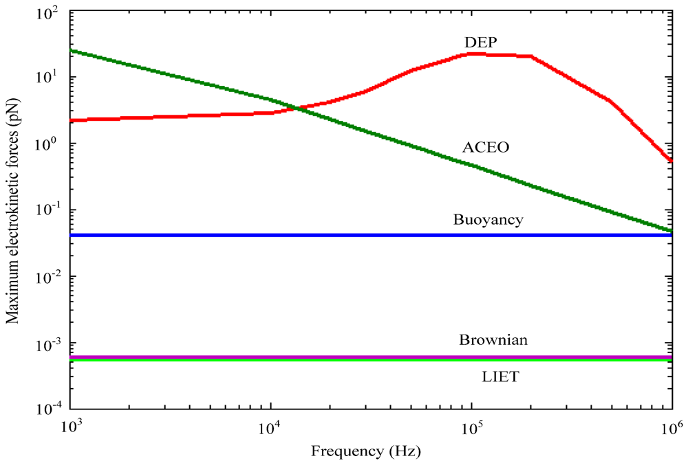
2. ODEP Force and Its Dependence on Optical Spectrum and Electric Field Waveform

A three-dimensional view of the geometry of the ODEP chip used in our simulation and experiments is shown in Figure 1(a). The device consists of a sandwich structure, including a top glass substrate coated with transparent and conductive indium tin oxide (ITO) film that is used as an electrode; a liquid layer containing the objects to be manipulated; and a bottom layer with a thin photoconductive film of a-Si:H deposited onto another ITO glass substrate. Unlike conventional DEP chips, no metal electrodes are required to generate the non-uniform electric field. Instead, the photoconductive a-Si:H film is used to “generate” localized virtual electrodes through its interaction with incident light. That is, when no incident light is present, most of the applied voltage drops across the a-Si:H layer because the a-Si:H has a dark conductivity of 10−11 S/m. The a-Si:H therefore behaves as an insulator in the dark. When an incident light beam illuminates the a-Si:H layer, the conductivity for the illuminated region of this layer sharply increases by several orders of magnitude because of the photon-generated electron-holes that increase the conductivity of the a-Si:H film. Thus, most of the applied voltage potential is then dropped across the liquid layer, creating a localized virtual electrode and generating a non-uniform electric field. The interaction between the optically-induced non-uniform electric field and objects in the liquid layer generates the DEP force, which is defined as the “ODEP force” in this case.
Figure 1. (a) Illustration of the trapping of microparticles by an image projected onto an optically-induced dielectrophoretic (ODEP) chip. The particles are attracted to the illuminated “ring” when initially experiencing a positive dielectrophoresis (DEP) force. After entering the “ring”, a negative ODEP force pushes the particles inward and hence the particles are trapped in the “ring”; (b) Simulation results showing the positive DEP force vectors exerted on a 10 μm Melan-a cell by the light ring when the liquid conductivity is 1 × 10⁻³ S/m (experimental value of an actual bio-fluid for Melan-a cells vibility) using an AC frequency of 30 kHz; (c) The negative DEP force vectors on 10 μm polystyrene beads by the light ring when the liquid conductivity is 9 × 10⁻³ S/m (experimental value for DI water) with a frequency of 30 kHz. The dark conductivity of the a-Si:H is 1 × 10⁻¹¹ S/m and the photo conductivity is 4 × 10⁻⁵ S/m (experimental values measured for the a-Si:H film used in our work) for the simulation results shown in (b) and (c).
Micromachines 03 00492 g001
The magnitude and directions of the generated ODEP force depend on several physical factors, which are briefly described as follows. The time-averaged DEP force exerted on a sphere in a fluidic medium is given as [20]:
Micromachines 03 00492 i001
where R is the particle radius, εm denotes the permittivity of the liquid medium, Micromachines 03 00492 i009 is the gradient of the energy density of the electric field, and K(ω) the Clausius-Mossotti (CM) factor, expressed as:
Micromachines 03 00492 i002
In the above equation, ε* = ε–jσ/ω, where ε and σ are the permittivity and conductivity, respectively; ω = 2πf, where f is the applied voltage frequency across the liquid medium. The subscripts p and m denote the properties of the particle and liquid medium, respectively. The DEP force acting on a particle can be positive or negative, depending on the sign of the real part of the CM factor. For example, when the same ODEP parameters are applied onto a polystyrene bead and a biological cell of equal radius, the DEP force vector exerted on them can be very different (as shown in the simulation results in Figure 1(b,c), due to their difference in material permittivity and the liquid medium permittivity (i.e., instead of DI water for beads, cells need to reside in specific bio-fluids in order to survive). If a particle is attracted to a region of higher electric field, it is said to be “pulled” by a positive DEP force, whereas if the particle is pushed toward a region of lower electric field, it is said to be “pushed” by a negative DEP force.

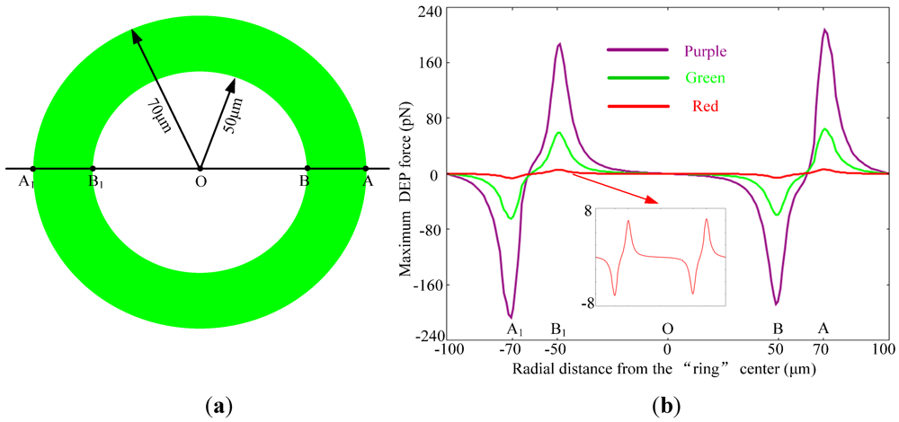
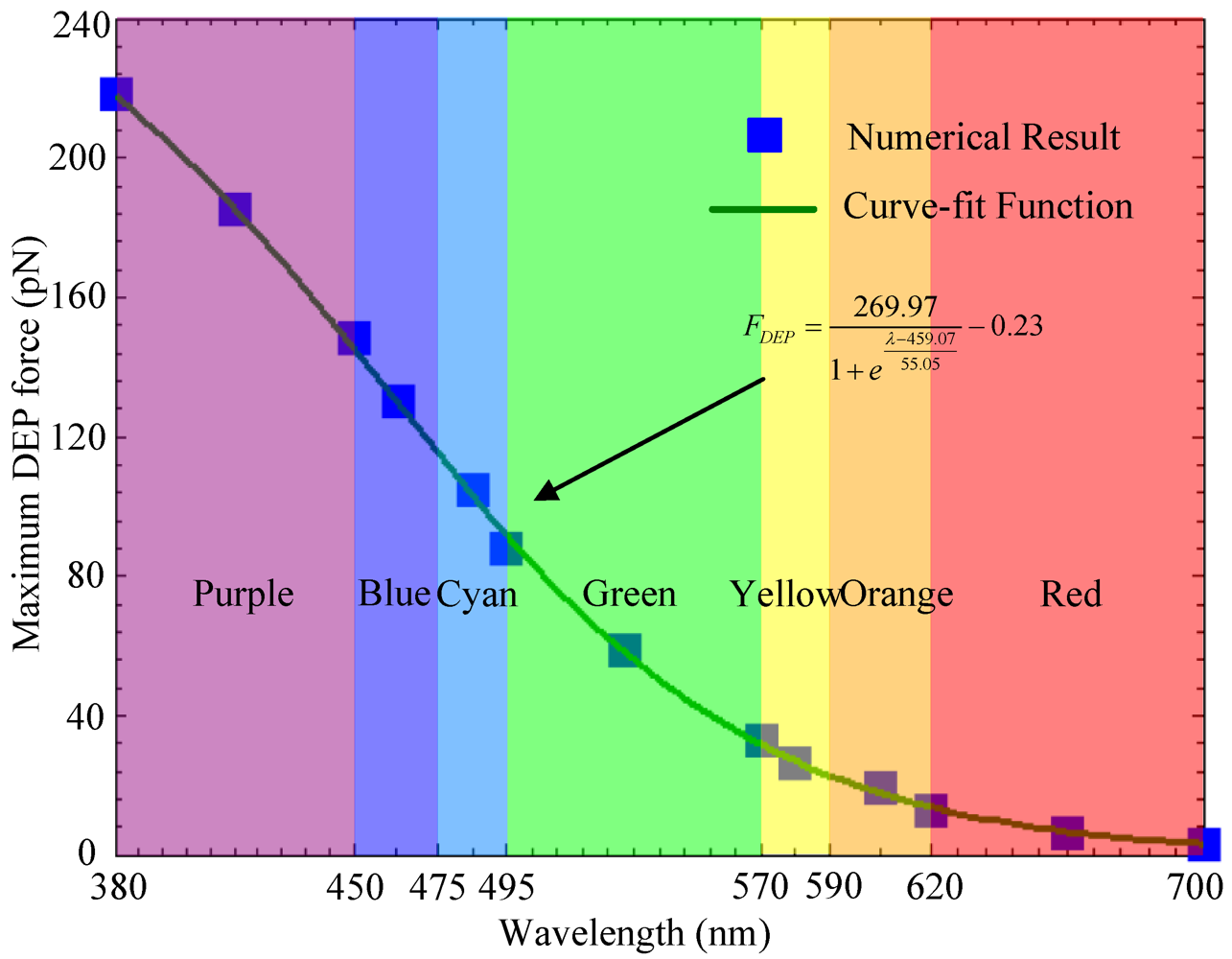
2.1. Optical Spectrum-Dependent ODEP Force
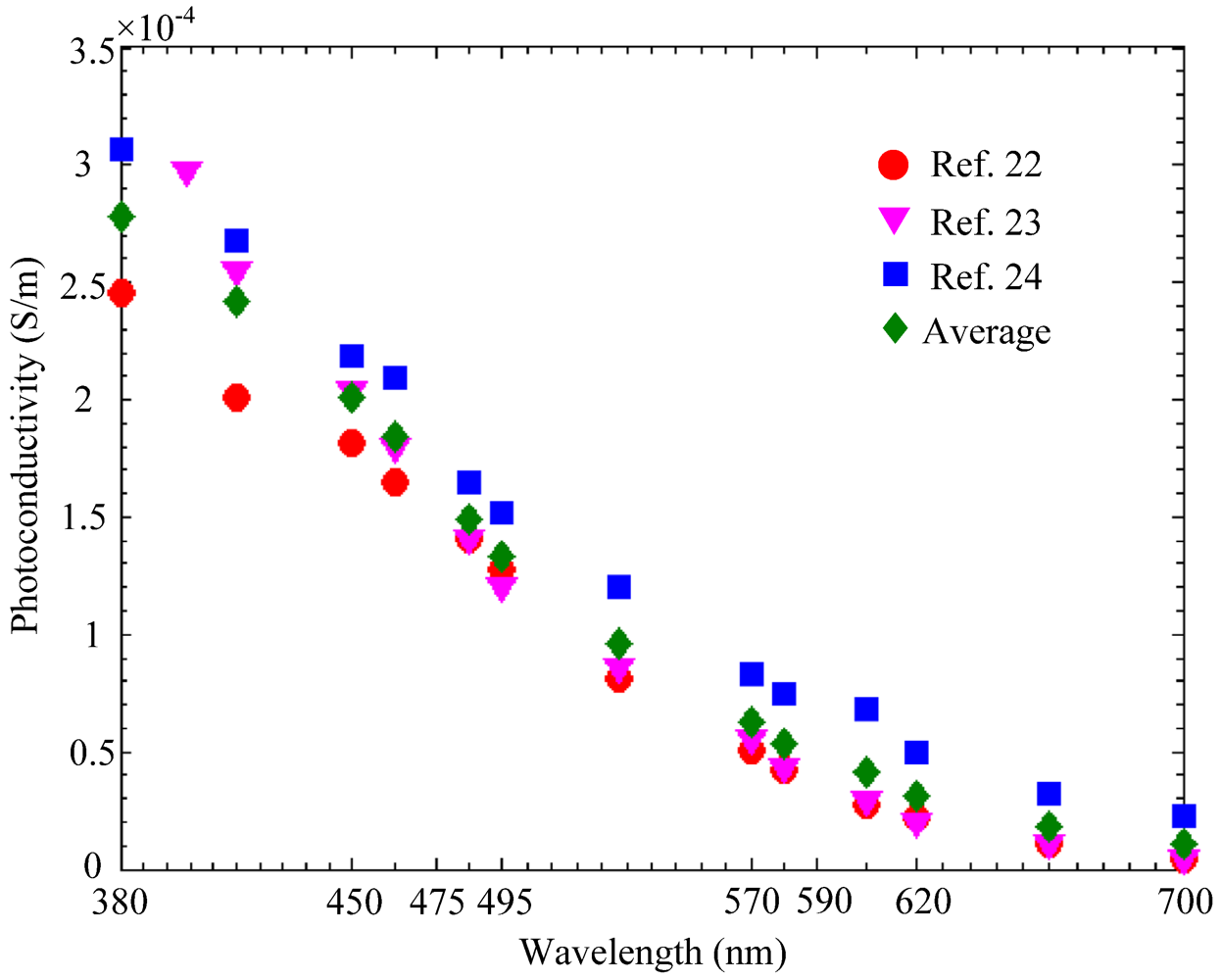
The absorption coefficient of the a-Si:H is proportional to illumination intensity [21] and also increases non-linearly with increasing incident optical frequency [22,23,24]. In addition, under different light colors (i.e., optical spectrum), the a-Si:H exhibits a different response in exciting the generated electron-hole pairs, i.e., the conductivity of the a-Si:H film on the ODEP chip will change as a function of incident optical spectrum. The general dependence of the a-Si:H film’s photoconductivity on incident light can be described by the following relationship [25]:
Micromachines 03 00492 i003
where e is the electron charge (e = 1.6 × 10⁻¹⁹ C), α represents the absorption coefficient of the a-Si:H, β is the number of the pairs of the excited electron-hole per absorbed photon (β = 1), μn denotes the mobility of the electron, τn is the life of the electron (μnτn = 10−7 cm2·V−1[26]), S is the optical power, h is the Planck’s constant (h = 6.63 × 10⁻³⁴ J·s), and fl is the frequency of light projected onto the a-Si:H film. Hence, from Equation (3) above it is clear that the ratio of (α/fl) governs the change of conductivity of the a-Si:H film, assuming all other factors in Equation (3) remain constant. By using Equation (3) and averaged experimental data for the absorption coefficient published by others (from [22,23,24]), we have tabulated the change of photoconductivity of the a-Si:H film as a function of incident optical wavelength, and the results are shown in Table 1. As shown, the film’s photoconductivity will increase with decreasing wavelength, i.e., by increasing the optical frequency (from red to green and then to purple color) of incident light onto the a-Si:H film will increase the film’s conductivity. Note, in tabulating the results for Table 1, we used an optical power S = 0.2 mW/cm2 in Equation (3). This value was measured using an optical power meter (JWD 1000 from Joinwit Optoelectronic Tech. Co. Ltd., China), which was placed at the same location where an ODEP chip typically is positioned (under a microscope lens) during our experimental work. We have also plotted the extracted data of absorption coefficients from [22,23,24], along with the averaged values from these references, in Figure 2 below. This is to show that the general trend of absorption coefficient as a function of optical wavelengths is similar from these references, and hence we chose to use their averaged values in calculating photoconductivity as a function of wavelength.
Table 1. Photoconductivity of the a-Si:H as a function of different light colors.
ColorWavelength (nm)Averaged Absorption Coefficient (m−1) Photoconductivity (S/m)
RedMax: 7001 × 1061.1 × 10−5
Mean: 6601.7 × 1061.8 × 10−5
Min: 6203.1 × 1063.1 × 10−5
OrangeMean: 6054.3 × 1064.2 × 10−5
YellowMean: 580 5.7 × 1065.3 × 10−5
GreenMax: 5706.8 × 1066.3 × 10−5
Mean: 5301.1 × 1079.6 × 10−5
Min: 4951.7 × 1071.3 × 10−4
CyanMean: 4851.9 × 1071.5 × 10−4
BlueMean: 4632.5 × 1071.8 × 10−4
PurpleMax: 4502.8 × 1072.0 × 10−4
Mean: 4153.6 × 1072.5 × 10−4
Min: 380 *4.5 × 107 *2.9 × 10−4
* Note: This averaged value was calculated based the absorption coefficient of a-Si:H at 380 nm from [22] and [24] and at 400 nm from [23].)
Figure 2. Absorption coefficient of a-Si:H vs. optical wavelength from several references.
Micromachines 03 00492 g002
Using the values of the photoconductivity from Table 1, the relationship between ODEP force generated in an ODEP chip and the wavelength of incident light was obtained by finite element method utilizing Comsol, a commercial finite element software. The time-harmonic analysis module, assuming Quasi-static current field with 2D axial symmetry, in Comsol was used to solve Maxwell’s equations in the sub-domain of the liquid chamber of the ODEP chip. The simulation geometry and its corresponding boundary settings are the same as those discussed in our prior work in [27]. Figure 3 shows the simulation results for the purple, green, and red incident lights of a “ring” shape geometer. As shown in the figure, the purple incident light can induce a higher DEP force than the red incident light. As discussed earlier, DEP force field exists throughout the liquid medium inside the ODEP chip when a light pattern is projected onto the a-Si:H layer and an AC potential is applied across the liquid medium. However, maximum DEP force is exerted on a particle when the particle is located on the a-Si:H film surface. Figure 3(b) shows the DEP force distribution on a 10 μm polystyrene bead at 5 μm height above the a-Si:H film surface for various projected image colors. The peak value of each curve indicates the location on the projected “ring” image where maximum DEP force occurs. The analysis above is repeated for various colors of visible light.
In general, as shown in Figure 4, we have found that ODEP force should decrease with increasing projected optical wavelength (or it should increase with increasing optical frequency) following the Fermi-Dirac Function, which validates that the optically-induced dielectrophoresis force depends strongly on the electron-hole carrier generation phenomena in optoelectronic materials.
Figure 3. (a) Incident light ring geometry; (b) Maximum DEP force for a 10 μm polystyrene bead with respect to different light colors. To obtain the numerical results, we have used the experimental dark conductivity of the a-Si:H film of 1 × 10⁻¹¹ S/m (measured by a Keithley 2410 source meter) and liquid conductivity of 9 × 10⁻³ S/m (measured by a Cond 3110 conductivity meter). The estimated photoconductivity values of the a-Si:H at the respective wavelengths from Table 1 are used in the simulation. The frequency of the applied AC potential is 30 kHz.
Micromachines 03 00492 g003
Figure 4. Maximum DEP force acting on a 10 μm polystyrene bead with respect to different light colors (optical wavelength). The simulation conditions are exactly the same as those given in Figure 3. The results indicate that the maximum DEP force decreases with increasing optical wavelength following the Fermi-Dirac Function ( Micromachines 03 00492 i010).
Micromachines 03 00492 g004

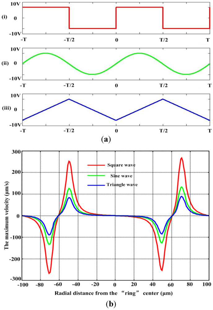
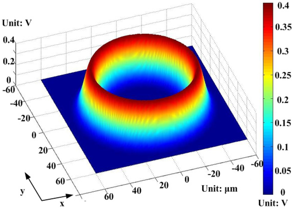
2.2. Dependence of ODEP Force on AC Electric Field Waveforms

As reported by many research groups (e.g., see [1,4,11]), an AC source with a sine function waveform is typically used to power ODEP devices. In this section, we show that a square waveform can actually increase the optically-induced DEP force in ODEP chips.
As discussed in [27], the maximum velocity that a particle can be transported by an ODEP ‘trap’ is related to the Stokes’ drag force, i.e., as long as the ODEP force magnitude used to transport a particle is greater the fluidic drag force on the moving particle, then the particle will remain inside a ‘ring trap’ as conceptually illustrated in Figure 1; otherwise, the particle will not remain inside the ring trap and cannot be transported at will in an ODEP chip. Furthermore, since Stokes’ drag force is directly proportional to the particle’s moving velocity, then the magnitude of ODEP force acting on a particle can be experimentally inferred if the velocity at which the particle ‘escapes’ the ring trap is measured. We define in this paper the maximum moving velocity above which a particle will escape from the ring trap as the ‘maximum velocity’ of a moving particle under certain ODEP parameters. The theoretical relationship between this maximum velocity and the applied AC electric field across the fluidic medium in an ODEP chip is presented below. Experimental results that validate this relationship are presented in the next section.
The maximum velocity of a particle due to an ODEP force field can be obtained by balancing the ODEP force and Stokes’ drag as discussed in [27]. Stokes’ drag formula for estimating the drag force on a particle moving in a fluid of dynamic viscosity η with velocity υ is given as:
Micromachines 03 00492 i004
Then, Equations (4) to (1) and solving the velocity υ yields the following expression for the critical particle velocity vc at which the ODEP force acting on the particle is equal to the Stokes’ drag force. That is, when a particle is manipulated at a velocity higher than the velocity given by Equation (5), an ODEP force field “trap” may become ineffective in moving a particle, i.e., a moving “ring” image cannot manipulate a particle effectively.
Micromachines 03 00492 i005
Equation (5) also shows that the maximum velocity at which a particle can be trapped by DEP force is directly related to the value of the applied voltage V across the liquid medium. That is,
Micromachines 03 00492 i006
Now, the RMS value of any periodical signal can be obtained by the following Equation [28]:
Micromachines 03 00492 i007
where u indicates the periodic signal, and T represents its cycle. For the square wave, the sine wave and the triangular wave with the same peak-to-peak voltage value of 20 V, and the same frequency of 30 kHz (as plotted in Figure 5(a)), their RMS values calculated using Equation (7) are 10 V, 10/sqrt(2) V, 10/sqrt(3) V, respectively. Thus, the ratio of the magnitude of maximum velocity generated by the three waveforms is (by substituting (7) into (5)):
Micromachines 03 00492 i008
Hence, theoretically, a square wave AC potential across the liquid medium can generate twice the magnitude of DEP force than sine wave AC potential, as shown in Figure 5(b).
Figure 5. (a)Waveforms of the (i) square wave, (ii) sine wave, and (iii) triangular wave with the same peak-to-peak voltage of 20 V and frequency of 30 kHz (T = 1/30 ms in the figure); (b) Numerical results of the maximum velocity induced by the DEP force acting on a 10 μm polystyrene bead with respect to the three waveforms utilizing the same “ring” image geometry shown in Figure 2(a). For these results, we have assumed a “green color ring”, and used the experimental dark conductivity of the a-Si:H at 1 × 10⁻¹¹ S/m, and photoconductivity at 4 × 10⁻⁵ S/m (measured by a Keithley 2410 Source Meter). Also, the experimental liquid conductivity used is 9 × 10⁻³ S/m (measured by a Cond 3110 conductivity meter).
Micromachines 03 00492 g005
Figure 6 shows the voltage distribution on a a-Si:H surface when a ring-shape light pattern is projected onto the surface, while a peak-to-peak voltage of 20 V is applied between the two ITO surfaces of an ODEP chip. The simulation geometry and parameters used to obtain this distribution are the same as those given in Figure 3(a), and the corresponding boundary settings are the same as those provided in [27]. The simulation result indicates that the voltage is higher at the edge of the ring and ~0 V at the inner part of the virtual electrode (i.e., “ring trap”).
Figure 6. Simulated potential voltage distribution for the “light trap” used in our experiments as the virtual electrode.
Micromachines 03 00492 g006
We note here that there are several AC related electrokinetic phenomena in an ODEP device, including the DEP force, light-induced electrothermal effect (LIET) [29], and ACEO. In addition, other physical phenomena such as Brownian motion [30] and buoyancy force [29] may also affect the motion of particles and fluid in an ODEP chip. When we select a specific frequency for the AC voltage potential between the two ITO surfaces of an ODEP chip to manipulate micro/nano particles, one of the above mentioned AC electrokinetic phenomena may dominate the manipulation process. Thus, ODEP-based manipulation has the additional advantage of being AC voltage frequency dependent, thereby offering an additional degree of freedom for trapping, manipulating, sorting, separating, and concentrating particles in micro/nano fluidic systems. For this study, the numerical solution for several electrokinetic phenomena (i.e., LIET and ACEO) were obtained using Comsol and MATLAB, with the same simulation parameters as those in [31], except that a liquid conductivity of 9 × 10⁻³ S/m and a Vp-p of 20 V were used to reflect the experimental conditions that will be discussed in Section 3. Figure 7 shows the results of electrokinetics analysis for a 10 μm polystyrene bead, which indicates that DEP force dominates the micro-manipulation process when the applied frequency is higher than ~15 kHz (given the conditions stated above). This is why we have used an AC frequency of 30 kHz in our experiments (as will be discussed in Section 3) and in simulation parameters in Figure 1, Figure 2, Figure 3, i.e., to ensure that dielectrophoresis is the main electrokinetic phenomenon governing the motion of the particles.
Figure 7. Electrokinetics analysis for a 10 μm polystyrene bead, which shows that the DEP force dominates the micro-manipulation process when the applied frequency is higher than ~15 kHz. Here, we have assume deionized water is the liquid medium at room temperature, with k = 0.6 J·m−1·s−1·K−1, ρm = 1 g·cm−3, α = −0.4% K−1, β = 2% K−1, and ∂ρm/∂T/ρm = 10−4 K−1.
Micromachines 03 00492 g007

3. Experimental Results

3.1. ODEP Force Dependence on AC Waveforms

We have performed several experiments using the ring-shape light pattern as a virtual electrode (as illustrated in Figure 3(a)), and successfully generated ODEP force to manipulate a single 10 μm polystyrene bead utilizing the square wave, sine wave, and triangular wave to power the ODEP chip (Figure 8(a–c)). Initially, the light pattern was projected onto the photoconductive layer through an objective lens attached to a projector, and no voltage potential was applied across the liquid medium (e.g., Figure 8a(i)). When an external square wave AC voltage potential with a peak-to-peak value of 20 V is applied, and the stage on which the ODEP chip is placed moves at a velocity of 50 μm/s, the bead can be trapped and moved along with the stage velocity (Figure 8a(ii)). As long as the stage velocity is below the velocity at which the Stokes’ drag force is equal to the induced DEP force, the bead remains trapped in the ring (i.e., as shown in Figure 8a(iii), where the velocity is 250 μm/s). When the velocity of the stage exceeds 260 μm/s, the bead remains behind the ring, i.e., it becomes “untrapped” (Figure 8a(iv); repeated experiments for the experimental configuration as shown in Figure 8(a) indicate that 260 μm/s is the maximum velocity at which the bead becomes “untrapped”). The experimental process using the sine wave and triangular wave AC potential to power the ODEP chip is the same as the above described process, and the maximum velocities for the sine wave and triangular waves are 140 and 85 μm/s, respectively. These experiments show that the ratio of the maximum velocity for the manipulation of a single polystyrene bead utilizing the square wave, sine wave, and triangular wave, respectively, is 6.1:3.3:2, which is similar to the theoretical results predicted by Equation (8) and Figure 5(b).
Figure 8. Experimental process of the ODEP manipulation of a 10 μm polystyrene bead using the square wave (a); sine wave (b); and triangular wave (c). (a) (i): No bias voltage was applied across the liquid medium; (ii): Bias voltage was applied and the stage on which the ODEP chip is placed moves at a velocity of 50 μm/s; the bead is trapped in the “ring” as it moves; (iii): The velocity of the stage increases to 250 μm/s, and the bead remains trapped; (iv): The bead lags behind when the velocity of the stage exceeds 260 μm/s; (b) Steps in (i) and (ii) are the same as those explained in (a); (iii): The velocity of the stage is increased to 135 μm/s; (iv): The bead lags behind when the stage velocity exceeds 140 μm/s; (c) Steps in (i) and (ii) are the same as those explained in (a); (iii): The stage velocity is increased to 80 μm/s; (iv): The bead lags behind when the stage velocity exceeds 85 μm/s. Thus the maximum velocities for manipulating a 10 μm bead utilizing the square wave, sine wave, and triangular wave are 260, 140, and 85 μm/s, respectively.
Micromachines 03 00492 g008

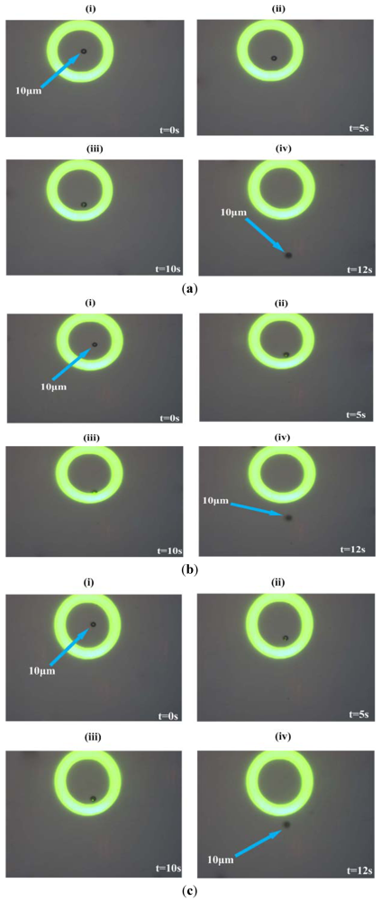
3.2. ODEP Force Dependence on Light Spectrum

Figure 9(a,b) shows the experimental results which confirm the theoretical prediction that higher frequency optical colors generate higher ODEP force in an ODEP chip (Figure 3(b)). The experimental processes shown in Figure 9(a,b) are similar. We take Figure 9(a) as an example to describe the experimental details. A green color ring was used as the external and stationary ring, while a purple color ring was used as an inner and moving ring. Both rings had equal width. These ring images were projected onto the photoconductive layer through an objective lens attached to a projector, and no voltage potential was initially applied across the liquid medium (Figure 9a(i)). Note that the purple color ring images were enhanced manually as the color filter and optical refraction of our microscope blur any non-green colors, i.e., only green rings are shown clearly in our ODEP microscope system. Then, a square wave AC bias voltage was switched on and the purple ring was continuously stretched outward. Experimentally, the 10 μm polystyrene beads were observed to be pushed toward the inner edge of the green ring, as shown in Figure 9a(ii). The beads stayed between the gap of the two rings when the distance of the gap is equal to or greater than the diameter of the beads (Figure 9a(iii)). Then, as the purple ring was further stretched to decrease the gap size, the beads were pushed through the green ring (Figure 9a(iv)), indicating that the ODEP force generated by the purple color ring is higher than that generated by the green color ring. Furthermore, the experimental results in Figure 9(b) indicate that the ODEP force induced by the green color is higher than that induced by the red color. These experimental observations qualitatively validate the theoretical prediction that higher frequency colors induce higher ODEP force.
Figure 9. (a) Experimental results showing that the magnitude of the ODEP force induced by a purple color ring is higher than that induced by a green color ring. (i): A purple color ring (as an inner and moving ring) and a green color ring (outer and stationary ring) were projected onto the ODEP chip and no bias voltage was applied; (ii): Bias voltage was switched on (20 Vp-p, 30 kHz, square wave) and the purple ring was continuously enlarged. Then, the 10 μm polystyrene beads were pushed toward the inner edge of the green ring; (iii): The beads stayed between the gap of the two rings when the gap was equal to or greater than the diameter of the beads; iv: The purple ring continues to expand and pushes the bead through the green ring; (b) Experimental results for green and red rings using the process as described in (a). The experimental results confirm that higher frequency light colors can generate higher magnitude ODEP force. Note that the color ring images were enhanced manually as color filtering and optical refraction blurs any non-green colors, i.e., only green rings are shown clearly in our ODEP microscope system.
Micromachines 03 00492 g009

4. Conclusions

In this paper, two important factors that affect the magnitude of the DEP force generated in an ODEP chip are discussed and analyzed both theoretically and experimentally. The effects of AC potential waveforms across the liquid medium of an ODEP chip were analytically determined. Moreover, the effects of the optical spectrum of the projected image on the a-Si:H layer on an ODEP chip were obtained numerically utilizing the finite element software Comsol. Analytical results indicate that an AC square waveform potential applied across an ODEP chip can produce twice the magnitude of DEP force in an ODEP chip as compared to a sine waveform. Numerical results indicate that the maximum DEP force generated on an ODEP chip decreases with increasing optical wavelength of the projected image on the a-Si:H layer. This decreasing trend closely follows the Fermi-Dirac function. Both of these theoretical results were validated by experimental results, which are also presented in this paper.

Acknowledgments

This work is supported by a self-sponsored project of the State Key Laboratory of Robotics (No. 2009Z02). This project is also partially supported by the CAS/SAFEA International Partnership Program for Creative Research Teams. Wen J. Li would like to thank the City University of Hong Kong for providing partial support (Funding No.: 9610216) to this project. The authors would like to thank all the members of the Micro/Nano Automation Group of the State Key Laboratory of Robotics, SIA, CAS, for their valuable discussions and support.

References

  1. Chiou, P.Y.; Ohta, A.T.; Wu, M.C. Massively parallel manipulation of single cells and microparticles using optical images. Nature 2005, 436, 370–372. [Google Scholar] [CrossRef]
  2. Grier, D.G. A revolution in optical manipulation. Nature 2003, 424, 810–816. [Google Scholar]
  3. Wong, T.S.; Li, W.J. Bulk Carbon Nanotubes as Sensing Element for Temperature and Anemometry Micro Sensing. In Proceedings of the 16th IEEE International Conference Micro Electro Mechanical Systems, Kyoto, Japan, 19–23 January 2003; pp. 41–44.
  4. Lin, Y.H.; Lee, G.B. An integrated cell counting and continuous cell lysis device using an optically induced electric field. Sens. Actuat: B: Chem. 2010, 145, 854–860. [Google Scholar] [CrossRef]
  5. Lin, Y.H.; Lee, G.B. Optically induced flow cytometry for continuous microparticle counting and sorting. Biosens. Bioelectron. 2008, 24, 572–578. [Google Scholar] [CrossRef]
  6. Lin, Y.H.; Chang, C.M.; Lee, G.B. Manipulation of single DNA molecules by using optically projected images. Opt. Express 2009, 17, 15318–15329. [Google Scholar]
  7. Pauzauskie, P.J.; Jamshidi, A.; Valley, J.K.; Satcher, J.H.; Wu, M.C. Parallel trapping of multiwalled carbon nanotubes with optoelectronic tweezers. Appl. Phys. Lett. 2009, 95, 113104:1–113104:3. [Google Scholar]
  8. Lee, M.W.; Lin, Y.H.; Lee, G.B. Manipulation and patterning of carbon nanotubes utilizing optically induced dielectrophoretic forces. Microfluid. Nanofluid. 2010, 8, 609–617. [Google Scholar] [CrossRef]
  9. Jamshidi, A.; Pauzauskie, P.J.; Schuck, P.J.; Ohta, A.T.; Chiou, P.Y.; Chou, J.; Yang, P.D.; Wu, M.C. Dynamic manipulation and separation of individual semiconducting and metallic nanowires. Nature 2008, 2, 85–89. [Google Scholar]
  10. Jamshidi, A.; Neale, S.L.; Yu, K.; Pauzauskie, P.J.; Schuck, P.J.; Valley, J.K.; Hsu, H.Y.; Ohta, A.T.; Wu, M.C. Nanopen: Dynamic, low-Power, and light-actuated patterning of nanoparticles. Nano Lett. 2009, 9, 2921–2925. [Google Scholar]
  11. Hung, S.H.; Lin, Y.H.; Lee, G.B. A microfluidic platform for manipulation and separation of oil-in-water emulsion droplets using optically induced dielectrophoresis. J. Micromech. Microeng. 2010, 20, 1–8. [Google Scholar]
  12. Chiou, P.Y.; Ohta, A.T.; Jamshidi, A.; Hsu, H.Y.; Wu, M.C. Light-actuated AC electroosmosis for nanoparticle manipulation. J. Microelectromech. S 2008, 17, 525–531. [Google Scholar] [CrossRef]
  13. Hwang, H.; Park, J.K. Dynamic light-activated control of local chemical concentration in a fluid. Anal. Chem. 2009, 81, 5865–5870. [Google Scholar] [CrossRef]
  14. Hwang, H.; Park, J.K. Measurement of molecular diffusion based on optoelectrofluidic fluorescence microscopy. Anal. Chem. 2009, 81, 9163–9167. [Google Scholar] [CrossRef]
  15. Hwang, H.; Park, Y.H.; Park, J.K. Optoelectrofluidic control of colloidal assembly in an optically induced electric field. Langmuir 2009, 25, 6010–6014. [Google Scholar]
  16. Hwang, H.; Chon, H.; Choo, J.; Park, J.K. Optoelectrofluidic sandwich immunoassays for detection of human tumor marker using surface-enhanced Raman scattering. Anal. Chem. 2010, 82, 7603–7610. [Google Scholar] [CrossRef]
  17. Hwang, H.; Park, J.K. Rapid and selective concentration of microparticles in an optoelectrofluidic platform. Lab Chip 2009, 9, 199–206. [Google Scholar] [CrossRef]
  18. Ohta, A.T.; Chiou, P.Y.; Huan, L.P.; Sherwood, S.W.; Yang, J.M.; Lau, N.K.; Hsu, H.Y.; Jamshidi, A.; Wu, M.C. Optically controlled cell discrimination and trapping using optoelectronic tweezers. J. Sel. Top. Quantum 2007, 13, 235–243. [Google Scholar]
  19. Li, W.Y.; Lin, Y.H.; Lee, G.B. Separation of micro-particles utilizing spatial difference of optically induced dielectrophoretic forces. Microfluid. Nanofluid. 2010, 8, 217–229. [Google Scholar]
  20. Jone, T.B. Electromechanics of Particles; Cambridge University Press: New York, NY, USA, 1995; pp. 17–20. [Google Scholar]
  21. Stutzmann, M.; Jackson, W.B.; Tsai, C.C. Light-induced metastable defects in hydrogenated amorphous silicon: A system study. Phys. Rev. B 1985, 32, 23–47. [Google Scholar]
  22. Carlson, D.E.; Wronski, C.R. Amorphous silicon solar cell. Appl. Phys. Lett. 1976, 28, 671–673. [Google Scholar] [CrossRef]
  23. Hishikawa, Y.; Nakamura, N.; Tsuda, S.; Nakano, S.; Kishi, Y.; Kuwano, Y. Interference-free determination of optical absorption coefficient and the optical gap of amorphous silicon thin films. Jpn. J. Appl. Phys. 1991, 30, 1008–1014. [Google Scholar] [CrossRef]
  24. Adachi, S. Optical Properties of Crystalline and Amorphous Semiconductors: Materials and Fundamental Principles; Kluwer Academic Publishers: Boston, MA, USA, 1999; pp. 207–208. [Google Scholar]
  25. Liu, E.K. Semiconductor Physics, 6th ed; Publishing House of Electronics Industry: Beijing, China, 2005; pp. 333–335. [Google Scholar]
  26. Okamoto, H.; Kida, H.; Nonomura, S.; Fukumoto, K.; Hamakawa, Y. Mobility-lifetime product and interface property in amorphous silicon solar cells. J. Appl. Phys. 1983, 54, 3236–3243. [Google Scholar] [CrossRef]
  27. Liang, W.F.; Wang, S.E.; Qu, Y.L.; Dong, Z.L.; Lee, G.B.; Li, W.J. An Equivalent Electrical Model for Numerical Analyses of ODEP Manipulation. In Proceedings of the 6th IEEE International Conference Nano/Micro Engineered and Molecular Systems, Kaohsiung, Taiwan, 20-23 February 2011; pp. 825–830.
  28. Li, Q. Fundamentals of Circuit; Xi’an Jiaotong University Press: Beijing, China, 2004; pp. 132–134. [Google Scholar]
  29. Castellanos, A.; Ramos, A.; Gonzalez, A.; Green, N.G.; Morgan, H. Electrohydrodynamics and dielectrophoresis in microsystems: Scaling laws. J. Phys. D: Appl. Phys. 2003, 36, 2584–2597. [Google Scholar] [CrossRef]
  30. Zheng, L.F.; Li, S.D.; Brody, J.P.; Nakano, S.; Kishi, Y.; Kuwano, Y. Manipulating nanoparticles in solution with electrically contacted nano-tubes using dielectrophoresis. Langmuir 2004, 20, 8612–8619. [Google Scholar]
  31. Li, M.L.; Qu, Y.L.; Dong, Z.L.; Wang, Y.C.; Li, W.J. Limitations of Au particle nanoassembly using dielectrophoretic force-A parametric experimental and theoretical study. IEEE Trans. Nanotechnol. 2008, 7, 477–479. [Google Scholar]

