Nonlinear Dual-Phase Multiplexing in Digital Microfluidic Architectures

Abstract
: A 16 × 16 digital microfluidic multiplexer is demonstrated. The device makes use of dual-phase AC activation in a bi-layered electrode structure for actuating microdrops independently. A switching arrangement is employed to localize two out-of-phase AC waveforms in one overlapped region of the two-dimensional multiplexer grid. The superimposed AC waveforms overcome the threshold voltage for motion of a local microdrop. The demonstrated dual-phase activation and nonlinear threshold-based motion overcomes the previously-reported microdrop interference effect, as it successfully actuates individual microdrops in systems with multiple neighbouring microdrops. The device is demonstrated with an integrated centre-tap transformer using a 10.0 Vrms input voltage and minimal power consumption.1. Introduction
In recent years, microfluidic devices have begun to receive a great deal of attention [1-4]. Such structures can perform conventional laboratory analyses with significant practical advantages. These advantages include the potential for high throughput and sensitivity, enhanced portability, and greatly reduced power consumption. The benefits of microfluidic systems are brought about by the micron-scale of the devices and the ability to manipulate microlitre and nanolitre fluid volumes. Such lab-on-a-chip structures are now finding applications in numerous biotechnology applications (e.g., enzymatic analysis [5], DNA analysis [6]), and proteomics [7]), clinical diagnostics [8,9], and pharmaceutical research [10].
An interesting subset of microfluidic technology has emerged in recent years by way of digital microfluidic systems [11-15]. These devices can provide two-dimensional microdrop actuation on a generalised platform—in contrast to in-line and one-dimensional flow channels [16]. Dynamic control in these digital implementations is instead based upon an electric-field-induced modification of interfacial surface tensions [17]. Voltages are applied at desired locations throughout the chip to initiate this electric field perturbation and dynamically control the fluid flow. Ultimately, the benefits of digital microfluidic architectures are seen by the fact that these processes are entirely reconfigurable and lend themselves to software-based sensing/actuation for a wide variety of fluid control applications.
Digital microfluidic devices are typically implemented as droplet-based systems. The most general form for these on-chip operations, with the highest level of actuation freedom, is the two-dimensional square electrode grid [18,19]. Voltages are applied to individual square electrodes in a plane to draw microdrops into their neighbouring minimum energy positions. This square electrode grid has the benefit that it can be applied to actuate microdrops in systems with multiple microdrops being present. On the other hand, such a configuration has practical limitations when implemented as an exceedingly large matrix. Grid structures beyond 5 × 5 [19] can become difficult to design and fabricate on the plane of the chip (if one wishes to avoid fabrication with underlying via holes). Each individual square electrode requires a separate electrical address line/input which must be patterned onto the actuating plane without crossing neighbouring electrodes or address lines. The design and fabrication of such a layout can therefore become difficult or even impossible for exceedingly small square electrodes and/or massively parallel architectures.
To overcome the addressability issues of the square electrode structure an intriguing solution is often used, whereby a cross-referenced grid minimizes the number of electrode inputs by applying voltages to orthogonal upper row and lower column electrodes in a bi-layer structure. In essence, the address lines and actuating electrodes are the same structures, and the overall complexity of the system is greatly reduced. The remaining challenge for these cross-referenced grid structures is, however, the initiation of undesired microdrop motion when multiple microdrops are present in the system. This undesired motion is the result of interference between microdrops that share common row/column electrodes. These interference challenges for the cross-referencing grid have been the focus of numerous analyses: Xiao et al. demonstrated a microdrop router to overcome electrode interference [20] and demonstrated Integer Linear Programming (ILP) to solve placement problems [21] and Xu et al. proposed a method of mapping the microdrop movement to the graph theory clique-partitioning problem [22]. These techniques offer methods to minimize the chances of microdrop interference when numerous microdrops are present, although such methods lead to an exponential increase in actuation complexity when attempting to avoid multiple microdrop interference.
In this paper, a new nonlinear localization method based upon a multiplexing grid and dual-phase excitation is introduced for actuating microdrops in a digital microfluidic system. The technique provides both the complete actuation freedom demonstrated by the square electrode grid (as locations in the two-dimensional plane can be individually addressed) and the minimal complexity of the cross-referenced grid (as the voltage inputs are only applied to linear row and column electrodes). This enhanced addressability with minimal inputs is brought about by the nonlinear localization of microdrop motion beyond a well-defined threshold voltage. This threshold voltage phenomenon is exhaustively analyzed by Renaudot et al. [23]. In our system, the desired microdrop is actuated by an above-threshold voltage only in the overlapped region of the upper row and lower column electrodes, while neighbouring microdrops remain below the threshold voltage value required for motion. The digital microfluidic multiplexer is demonstrated in this work with an integrated voltage transformer, giving AC dual-phase addressing onto the upper row and lower column electrodes. The system is driven by an input voltage of Vin = 10 Vrms, and actuation is demonstrated with multiple microdrops being present.
2. Architectures
Within this section, three generalized digital architectures are described for providing microdrop motion. The advantages and disadvantages of each system are discussed.
2.1. Square Electrode Grid
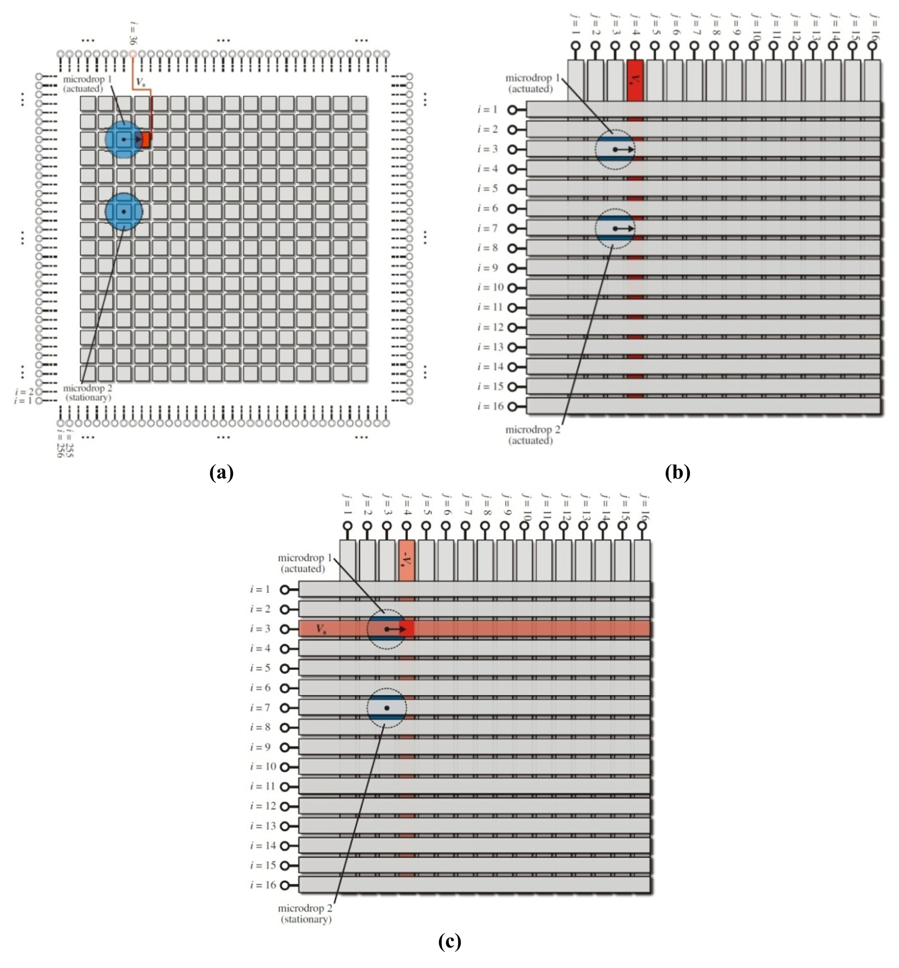
Digital microfluidic devices must apply spatially-defined voltage distributions to bring about the desired two-dimensional fluid motion. Ultimately, one wishes to have maximal control over this fluid flow, and the standard structure for applying the spatially-defined voltage distribution has been the two-dimensional electrode matrix with square electrodes arranged in M rows and N columns [18,19]. Such a structure is shown in Figure 1(a) with two microdrops on a 16 × 16 grid. When one wishes, for example, to actuate microdrop 1 and leave microdrop 2 stationary, the appropriate address line and square electrode can be activated with a sufficiently high voltage V0. This is shown in bright red in the figure. The resulting high electric field in this region leads to a modification of the local solid-liquid surface tension [17], and the microdrop is pulled toward this high field region. The microdrop moves to the right. This basic process can be continually carried out to dynamically direct the motion of numerous microdrops throughout this digital microfluidic architecture while leaving other microdrops stationary. It should be mentioned that the reconfigurable benefits of the two-dimensional square electrode grid are hampered, however, by practical limitations when one wishes to implement small electrode pitches or numerous row/column electrodes. A total number of M × N electrical address lines are needed from contact pads at the side of the chip, and these address lines must be routed in the plane between the square electrodes of the matrix (within the gaps) without crossing or overlapping the address lines. Thus large structures become impractical.
2.2. Cross-Referenced Grid
To alleviate the addressing complexity of the basic square electrode grid, an innovative cross-referenced architecture is sometimes used [20,21]. The cross-referenced grid avoids the use of square electrodes and uses, instead, M row electrodes and N column electrodes. Such a scenario is shown in Figure 1(b) with horizontal row electrodes (indexed with i) patterned onto the upper plane and vertical column electrodes (indexed with j) patterned onto the lower plane. Microdrops are located in the gap between these planes. For Figure 1(b), microdrops 1 and 2 are located at i = 3, j = 3 and i = 7, j = 3, respectively. A voltage is applied to the j = 4 column electrode (shown in bright red), and both microdrops are pulled toward the high field region on their right. Note that this motion is accomplished with the simplified cross-referenced geometry having only M + N inputs, as opposed to the M × N inputs of the same electrode grid, as the metallized lines in the cross-referenced grid operate effectively as both the address lines and actuating electrodes. Such a structure can therefore be scaled up for operation with larger numbers of row and column electrodes.
An additional complexity arises for cross-referenced digital microfluidic architectures when actuation of one microdrop is desired with multiple microdrops being present. Microdrops that share a common row or column will be simultaneously actuated, although the motion of both microdrops may not be desired. Such a scenario would occur for Figure 1(b) if it is desired that microdrop 1 move to the right while microdrop 2 is stationary. In its present form, the cross-referenced grid cannot accomplish this because of electrode interference. For these multi-microdrop systems, a digital microfluidic multiplexer grid can instead be employed.
2.3. Multiplexer Grid
The multiplexer grid makes use of the same physical structure as the cross-referenced grid. However, there are two additional design points addressed by the multiplexer grid: the unit is operated in a nonlinear actuation regime with a well-defined threshold voltage, and it is driven with bipolar voltage waveforms. The system is shown in Figure 1(c). Voltage actuation in this case is accomplished with two voltage signals. For the demonstrated scenario, +V0 is applied to the i = 3 upper row electrode and – V0 is applied to the j = 4 lower column electrode, where the positive variable V0 is the actuating voltage amplitude. This biasing creates a voltage difference between the upper and lower plates of V0 in all regions along the row and column electrodes, with the exception of the overlapped region where the voltage difference is 2V0. The nonlinear threshold voltage response for the onset of microdrop motion can then exploit this localized doubling of the voltage by way of a threshold voltage, Vth. The actuating voltage amplitude is selected such that V0 is less than the threshold voltage and 2V0 is greater than the threshold voltage (i.e., Vth/2 < V0 < Vth). For the system shown in Figure 1(c), microdrop 1 moves to the right, while microdrop 2 remains stationary. Such a system ultimately has M × N control with only M + N inputs and the capability to isolate an individual microdrop when multiple microdrops are present.
3. Theoretical Multiplexer Operation
3.1. Applied Voltages
The digital microfluidic multiplexer grid relates input applied voltages on row and column electrodes to the desired two-dimensional microdrop actuation. The voltage distribution on the upper row electrodes is denoted by Vi with the subscript i denoting the ith row electrode, and the voltage distribution on the lower column electrodes is denoted by Vj with the subscript j denoting the jth column electrode. The system contains M rows and N columns. For a particular case, an actuating voltage amplitude V0 is applied to the i = m row of the upper row electrodes, thus the corresponding spatial voltage distribution can be written as
Similarly, a voltage of −V0 is applied to the j = n column of the lower column electrodes, thus the corresponding spatial voltage distribution can be written as
Since the motion is induced by the internal electric field, it is the resulting local voltage differences between the upper row and lower column electrodes, Vij = Vi − Vj, which are important for motion, and the voltage differences can be expressed as
This voltage difference can then be related to the fluid capillary forces. The internal electric field modifies the local solid-liquid surface tension γsl from the nominal value of γsl,0. A discrete distribution of modified surface tensions, Δγij = γsl − γsl,0, is then found by way of the modified Lippmann equation,
The relationship between the applied voltage amplitude V0 and the threshold voltage Vth forms an important distinction in the operation of the device. For the standard cross-referenced grid, the electrodes are activated well above the threshold voltage, i.e., V0 ≫ Vth, which leads to a modified surface tension distribution of
It is important to note that such a result, representing the operation of a cross-referenced grid, can lead to inadvertent microdrop motion across the full i = m upper row and j = n lower column electrodes. This adds a heightened level of complexity for systems operating with multiple microdrops, as careful path planning, scheduling, and routing [24,25] will be required to avoid inadvertent actuation of neighbouring microdrops along the length of activated electrodes.
In contrast, the digital microfluidic multiplexer grid offers an opportunity to isolate motion at i = m, j = n if one intentionally selects the actuating voltage amplitude V0 to be within the range Vth/2 < V0 < Vth. With this inequality the modified surface tension distribution becomes
The distribution now activates only one location on the grid at the overlapped region of the m and n electrodes. At this specific location, the overall voltage is sufficient to overcome the threshold voltage needed for motion.
3.2. Threshold Voltages
The previous subsection concluded that actuation voltage amplitudes for digital microfluidic multiplexers must lie within the range Vth/2 < V0 < Vth. This is an intriguing actuation voltage condition, as it is in stark contrast to the simple inequality, Vth ≪ V0, observed for typical square electrode systems [18]. Standard digital microfluidic systems apply actuation voltages that are much larger than the device threshold voltage to overcome the inherent static friction forces and provide rapid microdrop transport. This desire for rapid droplet transport becomes far more complex for the digital microfluidic multiplexer, as there exists for V0 both a lower limit of Vth/2 and an upper limit of Vth. Clearly one cannot increase the multiplexer actuation voltage amplitude without bound. To provide rapid microdrop transport in a digital microfluidic system, it is necessary to understand the underlying nature of the threshold voltage, and such an understanding is the focus of this subsection.
Threshold voltages are a result of microdrop contact angle hysteresis [26,27], with the contact angle of interest being a function of the present electric field distribution and the microdrop's contact angle history (i.e., the microdrop profile exhibits irreversibility with voltage application). The difference between advancing and receding contact angles can be quantified by the empirical hysteresis angle, α, which characterizes the irreversibility brought about (mainly) by impurities and surface roughness. These anomalous surface characteristics lead to a non-zero hysteresis angle for advancing and receding microdrop conditions and the presence of a minimum voltage needed for actuation: the threshold voltage, Vth. The empirical quantity Vth is defined for each set of experimental conditions and/or device and can be linked to the hysteresis angle through the relation
The digital microfluidic multiplexer inequality Vth/2 < V0 < Vth suggests that large actuation voltage amplitudes can be applied for rapid microdrop transport only in a system with a sufficiently high threshold voltage Vth. This must be accomplished carefully, however. It would be to the disadvantage of the microdrop transport rates to increase the threshold through impurities and surface roughness, by way of the empirical parameter α in Equation (7), as these same characteristics would lead to dynamic frictional forces. As an alternative, one can employ a device with reduced capacitance per unit area, c, to allow for both ease of motion and a sufficiently high threshold voltage. The larger Vth value allows V0 to be increased, which in turn provides for a greater above-threshold voltage difference, 2V0 − Vth, in the localized actuation region of the two-dimensional grid. (Practical considerations for applying these higher electrode voltages are addressed with the phase-switched transformer technique introduced in Section 4).
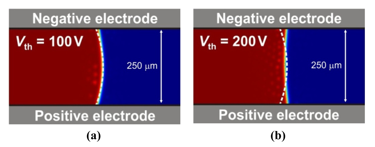
To visualize the role of threshold effects in microdrop actuation, finite-element modeling is used to characterize electrohydrodynamics in the device. The fluid dynamics are linked to electrostatic conditions with a multiphysics solver (COMSOL), and the results are shown in Figure 2 for systems with low and high threshold voltages.
Figure 2(a) shows an initial microdrop cross-section as a dashed-line, transformed to a final microdrop cross-section for a device with a small threshold voltage, Vth = 100 V. The actuation voltage amplitude is V0 = 0.6 Vth = 60 V, with −V0 applied to the upper electrode and +V0 applied to the lower electrode. In such a configuration, the microdrop witnesses a doubling of the actuation voltage amplitude, to 2V0 = 1.2 Vth, and a small contact angle deflection of Δθ = −8° is observed. The small contact angle deflection seen here is a result of the low threshold voltage and its fundamental limitations on the multiplexer's actuation voltage amplitude.
Figure 2(b) shows an initial microdrop cross-section as a dashed line, transformed to a final microdrop cross-section for the same multiplexer voltage biasing arrangement. In this second case, the system is modeled with an increased threshold voltage of Vth = 200 V, with V0 = 0.6 Vth = 120 V scaled up accordingly. A large contact angle deflection of Δθ = −28° is now observed. In this second case, the larger threshold voltage allows V0, and the voltage difference 2V0 − Vth, to create a greater transfer of electric field energy to microdrop kinetic energy. This increased microdrop deflection can then induce rapid transport.
Given the importance of the threshold-voltage in digital microfluidic multiplexers, the following section will address the practical design considerations and fabrication details for implementing such a system.
4. Device Design and Fabrication
The methodology introduced in the previous section for independently activating locations on the multiplexer grid can be implemented with a bipolar electrical biasing arrangement applying dual-phase AC waveforms. Such an arrangement would allow a predefined voltage to appear on a select upper row electrode with its opposite polarity on the appropriate lower column electrode.
Certain practical design details must be accommodated by the bipolar electrical biasing arrangement. In particular, the actuating voltage amplitude V0 being applied to the electrodes must be sufficiently large to initiate microdrop motion; at the same time, the input voltage into the device should be relatively low for integration with existing digital or transistor-transistor-logic (TTL) systems. These seemingly contradictory constraints can be met through the use of a voltage transformer, as highly insulating dielectric layers are included in the device design to limit the current and reduce the overall power consumption. A centre-tap transformer is chosen for this task as it provides an appreciable voltage gain (defined by the centre-tap turns ratio) and the capability for dual-phase AC outputs (the two centre-tap outputs are phase-locked with a fixed 180° phase difference).
For the digital microfluidic multiplexer assembled here, a centre-tap transformer (Hammond 117E4) is integrated into the design. An input voltage, Vin, at a frequency of 470 Hz is coupled into the two-wire transformer input. The unit provides a voltage gain of 75 at this frequency, and two AC waveforms with opposite polarity are extracted from the three-wire centre-tap output and then applied to the digital microfluidic multiplexer with a controlled switching scheme. A device schematic is shown in Figure 3. The AC waveform V0(0°) is controlled by the i-phase switch and is applied to upper row electrodes; the out-of-phase AC waveform V0(180°) is controlled by the j-phase switch and is applied to lower column electrodes. An overhead apochromatic microscope (LEICA APOZ6) is connected to a high-resolution camera (not shown) to record the motion of microdrops within this digital microfluidic multiplexer.
The digital microfluidic multiplexer undergoing testing is constructed as a 16 × 16 two-layered system with an upper row electrode plate and lower column electrode plate positioned with a separation of 1 mm. Electrodes on both of these silica plates are patterned from 50 nm thick copper films using UV photolithography (photoresist is spin-coated at 5,000 RPM, hard-baked for 60 minutes, UV-exposed with a 250 nm source, developed, and wet-etched in ferric chloride to produce the final features).This process leaves the multiplexer electrodes with a width of 550 μm and centre-to-centre pitch of 600 μm. After patterning, both plates are spin-coated (5,000 RPM) with an approximately 10 μm thick polydimethylsiloxane (PDMS) layer having a 1:10 ratio of silicone elastomer curing agent to silicone elastomer base then spin-coated (2,000 RPM) with a thin Teflon layer. The process leaves PDMS and Teflon layers uniform and homogeneous throughout the multiplexer grid. The completed overlapped electrode plates are shown in the upper left inset of Figure 3. The device is electrically bonded on the exterior bias pads shown on the periphery of the figure. The high resolution camera monitors the resulting microdrop motion, and the results are shown in the following section.
5. Results
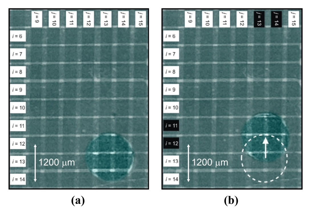
To begin investigating the operation of the digital microfluidic multiplexer, an experimental threshold voltage must be found. This is accomplished by positioning a microdrop with a diameter of 1,600 μm centred at i = 12.8, j = 13.4, where i row and j column fractions represent intermediate positions between electrodes. It is desired to translate this microdrop upward toward the intermediate position between the i = 11 and 12 pair and the j = 13 and 14 pair. These row and column electrodes are selected by phase-switching with V0(0°) onto the two row electrodes and V0(180°) onto the two column electrodes. The configuration is shown in Figure 4.
The input voltage is initially set to Vin = 0 Vrms and slowly increased. At an input voltage of Vin = 8.3 Vrms, the onset of motion is observed, corresponding to a threshold voltage on the chip of Vth = 620 Vrms. The initial microdrop position is shown in Figure 4(a), while the final microdrop position is shown in Figure 4(b). This threshold voltage defines the inequality Vth/2 < V0 < Vth for subsequent device testing. The actuating voltage amplitudes on the chip will be in the range 310 Vrms < V0 < 620 Vrms, while the device's input voltages, given by the transformer voltage gain of 75, will be in the range 8.3 Vrms < Vin < 16.6 Vrms.
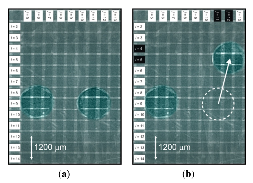
The fundamental capabilities for the digital microfluidic multiplexer lie in its ability to actuate a single microdrop without deflecting neighbouring microdrops. This capability is tested next with the two microdrop configuration shown in Figure 5(a).
Two microdrops with 1,700 μm diameter are positioned along the common i = 9 row electrode, with the left microdrop centred at j = 6 and the right microdrop centred at j = 11.3. An input voltage of Vin = 10.0 Vrms is applied to the device. With the appropriate phase-switching, this manifests itself as on-chip actuating voltage amplitudes of V0(0°) = 375 Vrms on the i = 4 and i = 5 electrodes and V0(180°) = 375 Vrms on the j = 11 and j = 12 electrodes. The result is shown in Figure 5(b). Given this biasing and switching arrangement, the right microdrop actuates to its final position at i = 4.8 and j = 12.1 with an average velocity of approximately 1.0 mm/s. Equally important to the rapid motion of the right microdrop, is the fact that the left microdrop remains completely stationary. Its current position does not have overlapped out-of-phase electrode voltages providing a doubling of the local field, thus it is unable to overcome the threshold for motion and it is successfully isolated from motion.
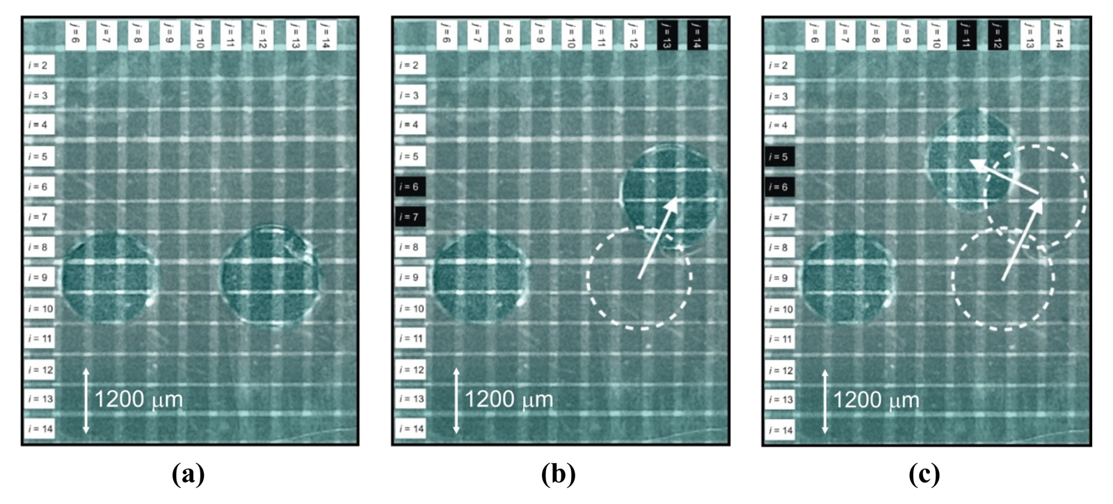
Figure 6 shows a heightened level of on-chip complexity for independent microdrop motion in the digital microfluidic multiplexer. Two-dimensional motion of the right microdrop in Figure 6(a) is demonstrated, with the left drop remaining stationary. Two microdrops with 2,000 μm diameter are initially positioned along the i = 9 row electrode, with the left microdrop centred at j = 7.2 and the right microdrop centred at j = 12.4. The input to the device is set at Vin = 10.0 Vrms, with phase-switching directing V0(0°) = 375 Vrms onto the i = 6 and i = 7 electrodes and V0(180°) = 375 Vrms onto the j = 13 and j = 14 electrodes. The right microdrop is actuated up and to the right, with a final position, i = 6.3 and j = 13.3, shown in Figure 6(b). The velocity for this actuation is approximately 1.0 mm/s. As a next step, the right microdrop is actuated up and to the left, with phase switching of V0(0°) = 375 Vrms onto the i = 5 and i = 6 electrodes and V0(180°) = 375 Vrms onto the j = 11 and j = 12 electrodes. The right microdrop actuates at an average velocity of 0.6 mm/s and arrives at the final position, i = 5.1 and j = 11.2, shown in Figure 6(c). The left microdrop is completely isolated from the independent and two-dimensional motion of the right microdrop during this entire process.
Droplet actuation throughout chip is found to be equally effective, suggesting that the chip is uniform and homogenous in both the electrode grid structure and hydrophobic/insulative layering. Microdrops with a variety of sizes could be actuated with electrodes in isolation or in groupings—with the optimal actuation grouping depending on the volume for the microdrop of interest. For the above investigations, with nanolitre microdrop volumes and an approximate volume dispensing error of 10%, electrode pairings were found to be the most effective.
6. Conclusion
Within this work, a 16 × 16 digital microfluidic multiplexer was introduced. The bi-layered device made use of voltage activation with a dual-phase AC biasing scheme. A switching arrangement was employed to localize these two out-of-phase AC waveforms in the multiplexer and initiate motion of a single microdrop within the device. One microdrop could be successfully actuated (beyond its threshold voltage), while neighbouring microdrops could be held stationary. Complete two-dimensional addressability was demonstrated with a 10.0 Vrms input voltage and minimal power consumption. The device was ultimately successful in eliminating multiple microdrop interference and can be applied in future digital microfluidic applications requiring small electrode sizes or scaling to massively parallel architectures. Potential applications of this device include bioassay processes [28], highly parallel planar mixing processes [29], DNA analyses [6], and glucose monitoring systems [30].


Acknowledgments
The authors wish to acknowledge financial support from the Natural Sciences and Engineering Research Council of Canada (NSERC).
References
- Khoo, H.S.; Lin, C.; Huang, S.-H.; Tseng, F.-G. Self-assembly in micro- and nanofluidic devices: A review of recent efforts. Micromachines 2011, 2, 17–48. [Google Scholar]
- Cheng, D.; Jiang, H. A debubbler for microfluidics utilizing air-liquid interfaces. Appl. Phys. Lett. 2009, 95, 214103:1–214103:3. [Google Scholar]
- Au, A.K.; Lai, H.; Utela, B.R.; Folch, A. Microvalves and micropumps for biomems. Micromachines 2011, 2, 179–220. [Google Scholar]
- Bardaweel, H.K.; Anderson, M.J.; Richards, R.F.; Richards, C.D. Optimization of the dynamic and thermal performance of a resonant micro heat engine. J. Micromech. Microeng. 2008, 18, 104014. [Google Scholar]
- Miyazaki, M.; Honda, T.; Yamaguchi, H.; Briones, M.P.P.; Maeda, H. Enzymatic processing in microfluidic reactors. Biotechnol. Genet. Eng. 2008, 25, 405–428. [Google Scholar]
- Humphreys, T.; Andersson, J.; Södervall, U.; Melvin, T. World-to-chip interconnects for efficient loading of genomic DNA into microfluidic channels. J. Micromech. Microeng. 2009, 19, 105024. [Google Scholar]
- Lee, J.; Soper, S.A.; Murray, K.K. Microfluidics with MAlDI analysis for proteomics—A review. Anal. Chim. Acta 2009, 649, 180–190. [Google Scholar]
- Li, T.; Zhang, L.; Leung, K.M.; Yang, J. Out-of-plane microvalves for whole blood separation on lab-on-a-CD. J. Micromech. Microeng. 2010, 20, 105024. [Google Scholar]
- Chandrappan, J.; Ruiqi, L.; Su, N.; Yi, G.H.Y.; Vaidyanathan, K. Thermo-mechanical actuator-based miniature tagging module for localization in capsule endoscopy. J. Micromech. Microeng. 2010, 21, 045037. [Google Scholar]
- Welch, C.J.; Sajonz, P.; Biba, M.; Gouker, J.; Fairchild, J. Comparison of multiparallel microfluidic HPLC instruments for high throughput analyses in support of pharmaceutical process research. J. Liq. Chrom. Rel. Technol. 2006, 29, 2185–2200. [Google Scholar]
- Fair, R.B. Digital microfluidics: Is a true lab-on-a-chip possible? Microfluid. Nanofluid. 2007, 3, 245–281. [Google Scholar]
- Zhao, Y.; Chakrabarty, K. On-line testing of lab-on-chip using reconfigurable digital-microfluidic compactors. Int. J. Parallel Prog. 2009, 37, 370–388. [Google Scholar]
- Beyzavi, A.; Nguyen, N.-T. Modeling and optimization of planar microcoils. J. Micromech. Microeng. 2008, 18, 095018. [Google Scholar]
- Chabreyrie, R.; Vainchtein, D.; Chandre, C.; Singh, P.; Aubry, N. Robustness of tuned mixing within a droplet for digital microfluidics. Mech. Res. Commun. 2009, 36, 130–136. [Google Scholar]
- Malic, L.; Veres, T.; Tabrizian, M. Nanostructured digital microfluidics for enhanced surface plasmon resonance imaging systems. Biosens. Bioelectron. 2011, 26, 2053–2059. [Google Scholar]
- Vestad, T.; Marr, D.W.M.; Oakey, J. Flow control for capillary-pumped microfluidic systems. J. Micromech. Microeng. 2004, 14, 1503–1506. [Google Scholar]
- Dolatabadi, A.; Mohseni, K.; Arzpeyma, A. Behaviour of a moving droplet under electrowetting actuation: Numerical simulation. Can. J. Chem. Eng. 2006, 84, 17–21. [Google Scholar]
- Maftei, E.; Pop, P.; Madsen, J. Tabu search-based synthesis of digital microfluidic biochips with dynamically reconfigurable non-rectangular devices. Des. Autom. Embed. Syst. 2010, 14, 287–307. [Google Scholar]
- Davids, D.; Datta, S.; Mukherjee, A.; Joshi, B.; Ravindran, A. Multiple fault diagnosis in digital microfluidic biochips. ACM J. Emerg. Technol. 2006, 2, 262–276. [Google Scholar]
- Xiao, Z.; Young, E.F.Y. CrossRouter: A Droplet Router for Cross-Referencing Digital Microfluidic Biochips. Proceedings of the 15th Asia South Pacific Design Automation Conference, Hong Kong, China, 18–21 January 2010; pp. 269–274.
- Xiao, Z.; Young, E.F.Y. Droplet-Routing-Aware Module Placement for Cross-Referencing Biochips. Proceedings of the 19th International Symposium on Physical Design, San Francisco, CA, USA, 14–17 March 2010; pp. 193–199.
- Xu, T.; Chakrabarty, K. A droplet-manipulation method for achieving high-throughput in cross-referencing-based digital microfluidic biochips. IEEE Trans. Comput.-Aided Design Integr. Circuits Syst. 2008, 27, 1905–1917. [Google Scholar]
- Renaudot, R.; Agache, V.; Daunay, B.; Lambert, P.; Kumemura, M.; Fouillet, Y.; Collard, D.; Fujita, H. Optimization of liquid dielectrophoresis (LDEP) digital microfluidic transduction for biomedical applications. Micromachines 2011, 2, 258–273. [Google Scholar]
- Yuh, P.-H.; Yang, C.-L. BioRoute: A network-flow-based routing algorithm for the synthesis of digital microfluidic biochips. IEEE Trans. Computer-Aided Design Integr. Circuits Syst. 2008, 27, 1928–1941. [Google Scholar]
- Ricketts, A.J.; Irick, K.; Vijaykrishnan, N.; Irwin, M.J. Priority Scheduling in Digital Microfluidics-Based Biochips. Proceedings of the Design, Automation and Test in Europe, Munich, Germany, 6–10 March 2006; pp. 329–334.
- Berthier, J. Microdrops and Digital Microfluidics, 1st ed.; William Andrew: Norwich, NY, USA, 2008; pp. 196–201. [Google Scholar]
- Ahmadi, A.; Najjaran, H.; Holzman, J.F.; Hoorfar, M. Two-dimensional flow dynamics in digital microfluidic systems. J. Micromech. Microeng. 2009, 19, 065003. [Google Scholar]
- Mulvaney, S.P.; Cole, C.L.; Kniller, M.D.; Malito, M.; Tamanaha, C.R.; Rife, J.C.; Stanton, M.W.; Whitman, L.J. Rapid, femtomolar bioassays in complex matrices combining microfluidics and magnetoelectronics. Biosens. Bioelectron. 2007, 23, 191–200. [Google Scholar]
- Zhang, K.; Guo, S.; Zhao, L.; Zhao, X.; Chan, H.L.W.; Wang, Y. Realization of planar mixing by chaotic velocity in microfluidics. Microelectron. Eng. 2011, 88, 959–963. [Google Scholar]
- Pereira Rodrigues, N.; Sakai, Y.; Fujii, T. Cell-based microfluidic biochip for the electrochemical real-time monitoring of glucose and oxygen. Sens. Actuat. B: Chem. 2008, 132, 608–613. [Google Scholar]
© 2011 by the authors; licensee MDPI, Basel, Switzerland. This article is an open access article distributed under the terms and conditions of the Creative Commons Attribution license (http://creativecommons.org/licenses/by/3.0/).
Share and Cite
Collier, C.M.; Wiltshire, M.; Nichols, J.; Born, B.; Landry, E.L.; Holzman, J.F. Nonlinear Dual-Phase Multiplexing in Digital Microfluidic Architectures. Micromachines 2011, 2, 369-384. https://doi.org/10.3390/mi2040369
Collier CM, Wiltshire M, Nichols J, Born B, Landry EL, Holzman JF. Nonlinear Dual-Phase Multiplexing in Digital Microfluidic Architectures. Micromachines. 2011; 2(4):369-384. https://doi.org/10.3390/mi2040369
Chicago/Turabian StyleCollier, Christopher M., Michael Wiltshire, Jacqueline Nichols, Brandon Born, Emily L. Landry, and Jonathan F. Holzman. 2011. "Nonlinear Dual-Phase Multiplexing in Digital Microfluidic Architectures" Micromachines 2, no. 4: 369-384. https://doi.org/10.3390/mi2040369
APA StyleCollier, C. M., Wiltshire, M., Nichols, J., Born, B., Landry, E. L., & Holzman, J. F. (2011). Nonlinear Dual-Phase Multiplexing in Digital Microfluidic Architectures. Micromachines, 2(4), 369-384. https://doi.org/10.3390/mi2040369