
All-Aluminum Thin Film Transistor Fabrication at Room Temperature

 , ,
, ,  , ,
, ,
Abstract
:
1. Introduction
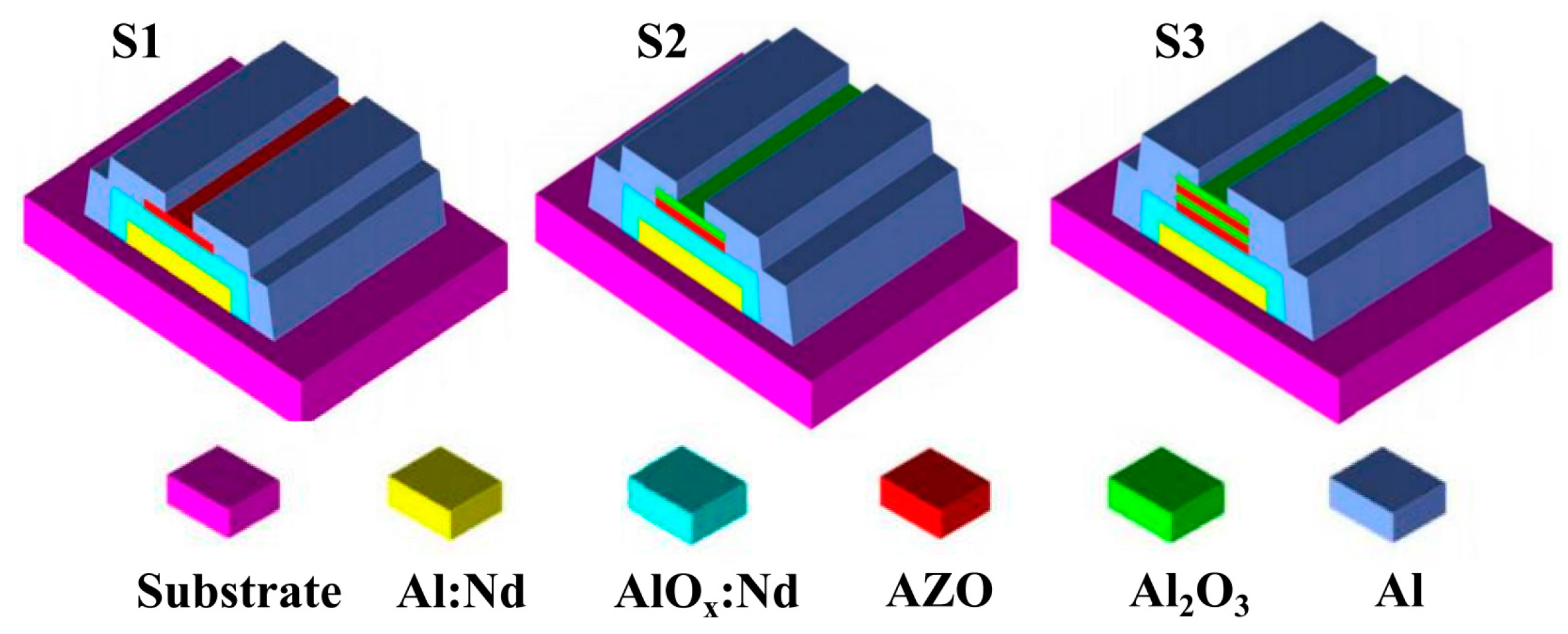
2. Experiments
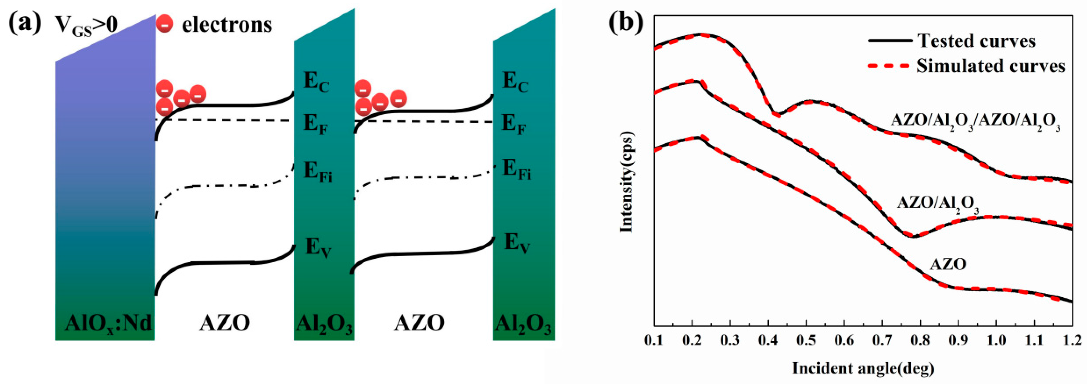
3. Results and Discussion
4. Conclusions
Acknowledgments
Author Contributions
Conflicts of Interest
References
- Kenji, N.; Ohta, H.; Takagi, A.; Kamiya, T.; Hirano, M.; Hosono, H. Room-temperature fabrication of transparent flexible thin-film transistors using amophous oxide semiconductors. Nature 2004, 432, 488–492. [Google Scholar]
- Jung, S.W.; Chae, S.S.; Park, J.H.; Oh, J.Y.; Bhang, S.H.; Baik, H.K.; Lee, T.I. Microscale soft patterning for solution processable metal oxide thin film transistors. ACS Appl. Mater. Interfaces 2016, 8, 7205–7211. [Google Scholar] [CrossRef] [PubMed]
- Yabuta, H.; Zhu, B.; Ast, D.G.; Greene, R.G.; Thompson, M.O. High-mobility thin-film transistor with amorphous InGaZnO4 channel fabricated by room temperature RF-magnetron sputtering. Appl. Phys. Lett. 2006, 89, 112123. [Google Scholar] [CrossRef]
- Park, J.S.; Maeng, W.; Kim, H.; Park, J. Review of recent developments in amorphous oxide semiconductor thin-film transistor devices. Thin Solid Films 2012, 520, 1679–1693. [Google Scholar] [CrossRef]
- Homola, T.; Buršíková, V.; Ivanova, T.V.; Souček, P.; Maydannik, P.S.; Cameron, D.C.; Lackner, J.M. Mechanical properties of atomic layer deposited Al2O3/ZnO nanolaminates. Surf. Coat. Technol. 2015, 284, 198–205. [Google Scholar] [CrossRef]
- Nayak, P.K.; Wang, Z.; Anjum, D.H.; Hedhili, M.N.; Alshareef, H.N. Highly stable thin film transistors using multilayer channel structure. Appl. Phys. Lett. 2015, 106, 103505. [Google Scholar] [CrossRef]
- Ahn, C.H.; Senthil, K.; Cho, H.K.; Lee, S.Y. Artificial semiconductor/insulator superlattice channel structure for high-performance oxide thin-film transistors. Sci. Rep. 2013, 3, 2737. [Google Scholar] [CrossRef] [PubMed]
- Lee, S.; Hwang, C.; Pi, J.; Yang, J.; Oh, H.; Cho, S.H.; Cho, K.; Chu, H.Y. Characterization of amorphous multilayered ZnO-SnO2 heterostructure thin films and their field effect electronic properties. Appl. Phys. Lett. 2014, 105, 201601. [Google Scholar] [CrossRef]
- Ahn, C.H.; Cho, H.K.; Kim, H. Carrier confinement effect-driven channel design and achievement of robust electrical/photostability and high mobility in oxide thin-film transistors. J. Mater. Chem. C 2015, 4, 727–735. [Google Scholar] [CrossRef]
- Park, J.H.; Alshammari, F.H.; Wang, Z.; Alshareef, H.N. Interface engineering for precise threshold voltage control in multilayer-channel thin film transistors. Adv. Mater. Interfaces 2016, 1600713. [Google Scholar] [CrossRef]
- Ahn, C.H.; Bo, H.K.; Kim, H.; Cho, H.K. Improved electrical stability in the Al doped ZnO thin-film-transistors grown by atomic layer deposition. J. Electrochem. Soc. 2011, 158, H170–H173. [Google Scholar] [CrossRef]
- Hua, X.; Luo, D.; Li, M.; Xu, M.; Zou, J.; Tao, H.; Lan, L.; Wang, L.; Peng, J.; Cao, Y. A flexible AMOLED display on the PEN substrate driven by oxide thin-film transistors using anodized aluminium oxide as dielectric. J. Mater. Chem. C 2014, 2, 1255–1259. [Google Scholar]
- Prabhakar, T.; Dai, L.; Zhang, L.; Yang, R.; Li, L.; Guo, T.; Yan, Y. Effects of growth process on the optical and electrical properties in Al-doped ZnO thin films. J. Appl. Phys. 2014, 115, 083702. [Google Scholar] [CrossRef]
- Kusayanagi, M.; Uchida, A.; Oka, N.; Jia, J.; Nakamura, S.; Shigesato, Y. Al-doped ZnO films deposited on a slightly reduced buffer layer by reactive dc unbalanced magnetron sputtering. Thin Solid Films 2014, 555, 93–99. [Google Scholar] [CrossRef]
- Hagendorfer, H.; Lienau, K.; Nishiwaki, S.; Fella, C.M.; Kranz, L.; Uhl, A.R.; Jaeger, D.; Luo, L.; Gretener, C.; Buecheler, S.; et al. Highly transparent and conductive ZnO: Al thin films from a low temperature aqueous solution approach. Adv. Mater. 2014, 26, 632–636. [Google Scholar] [CrossRef] [PubMed]
- Zan, H.; Yeh, C.C.; Meng, H.F.; Tsai, C.C.; Chen, L.H. Achieving high field-effect mobility in amorphous indium-gallium-zinc oxide by capping a strong reduction layer. Adv. Mater. 2012, 24, 3509–3514. [Google Scholar] [CrossRef] [PubMed]
- Seo, J.; Bae, B. Improved electrical performance and bias stability of solution-processed active bilayer structure of indium zinc oxide based TFT. ACS Appl. Mater. Interfaces 2014, 6, 15335–15343. [Google Scholar] [CrossRef] [PubMed]
- Jia, J.; Torigoshi, Y.; Kawashima, E.; Utsuno, F.; Yano, K.; Shigesato, Y. Amorphous indium-tin-zinc oxide films deposited by magnetron sputtering with various reactive gases: Spatial distribution of thin film transistor performance. Appl. Phys. Lett. 2015, 106, 023502. [Google Scholar] [CrossRef]
- Rembert, T.; Battaglia, C.; Anders, A.; Javey, A. Room temperature oxide deposition approach to fully transparent, all-oxide thin-film transistors. Adv. Mater. 2015, 27, 6090–6095. [Google Scholar] [CrossRef] [PubMed]
- Gupta, M.; Chowdhury, F.R.; Barlage, D.; Mosnier, J.-P. Optimization of pulsed laser deposited ZnO thin-film growth parameters for thin-film transistors (TFT) application. Appl. Phys. A 2013, 110, 793–798. [Google Scholar] [CrossRef]
- Inguva, S.; Vijayaraghavan, R.K.; McGlynn, E.; Mosnier, J.-P. Highly transparent and reproducible nanocrystalline ZnO and AZO thin films grown by room temperature pulsed-laser deposition on flexible Zeonor plastic substrates. Mater. Res. Express 2015, 2, 096401. [Google Scholar] [CrossRef]
- An, S.; Mativenga, M.; Kim, Y.; Jang, J. Improvement of bias-stability in amorphous-indium-gallium-zinc-oxide thin-film transistors by using solution-processed Y2O3 passivation. Appl. Phys. Lett. 2014, 105, 053507. [Google Scholar] [CrossRef]
- Choi, S.H.; Han, M.K. Effect of deposition temperature of SiOx passivation layer on the electrical performance of a-IGZO TFTs. IEEE Electron Device Lett. 2012, 33, 396–398. [Google Scholar] [CrossRef]
- Wu, J.; Chen, Y.; Zhou, D.; Hu, Z.; Xie, H.; Dong, C. Sputtered oxides used for passivation layers of amorphous InGaZnO thin film transistors. Mater. Sci. Semicond. Process. 2015, 29, 277–282. [Google Scholar] [CrossRef]
- Lin, Y.; Faber, H.; Labram, J.G.; Stratakis, E.; Sygellou, L.; Kymakis, E.; Hastas, N.A.; Li, R.; Zhao, K.; Amassian, A.; et al. High electron mobility thin-film transistors based on solution-processed semiconducting metal oxide heterojunctions and quasi-superlattices. Adv. Sci. 2015, 2, 1500058. [Google Scholar] [CrossRef] [PubMed]
- Fortunato, E.; Barquinha, P.; Martins, R. Oxide semiconductor thin-film transistors: A review of recent advances. Adv. Mater. 2012, 24, 2945–2986. [Google Scholar] [CrossRef] [PubMed]
- Calatayud, M.; Markovits, A.; Menetrey, M.; Mguig, B.; Minot, C. Adsorption on perfect and reduced surfaces of metal oxides. Catal. Today 2003, 85, 125–143. [Google Scholar] [CrossRef]
- Nomura, K.; Kamiya, T.; Hirano, M.; Hosono, H. Origins of threshold voltage shifts in room-temperature deposited and annealed a-In-Ga-Zn-O thin-film transistors. Appl. Phys. Lett. 2009, 95, 0135021. [Google Scholar] [CrossRef]
- Byungki, R.; Noh, H.; Choi, E.; Chang, K.J. O-vacancy as the origin of negative bias illumination stress instability in amorphous In-Ga-Zn-O thin film transistors. Appl. Phys. Lett. 2010, 97, 022108. [Google Scholar]


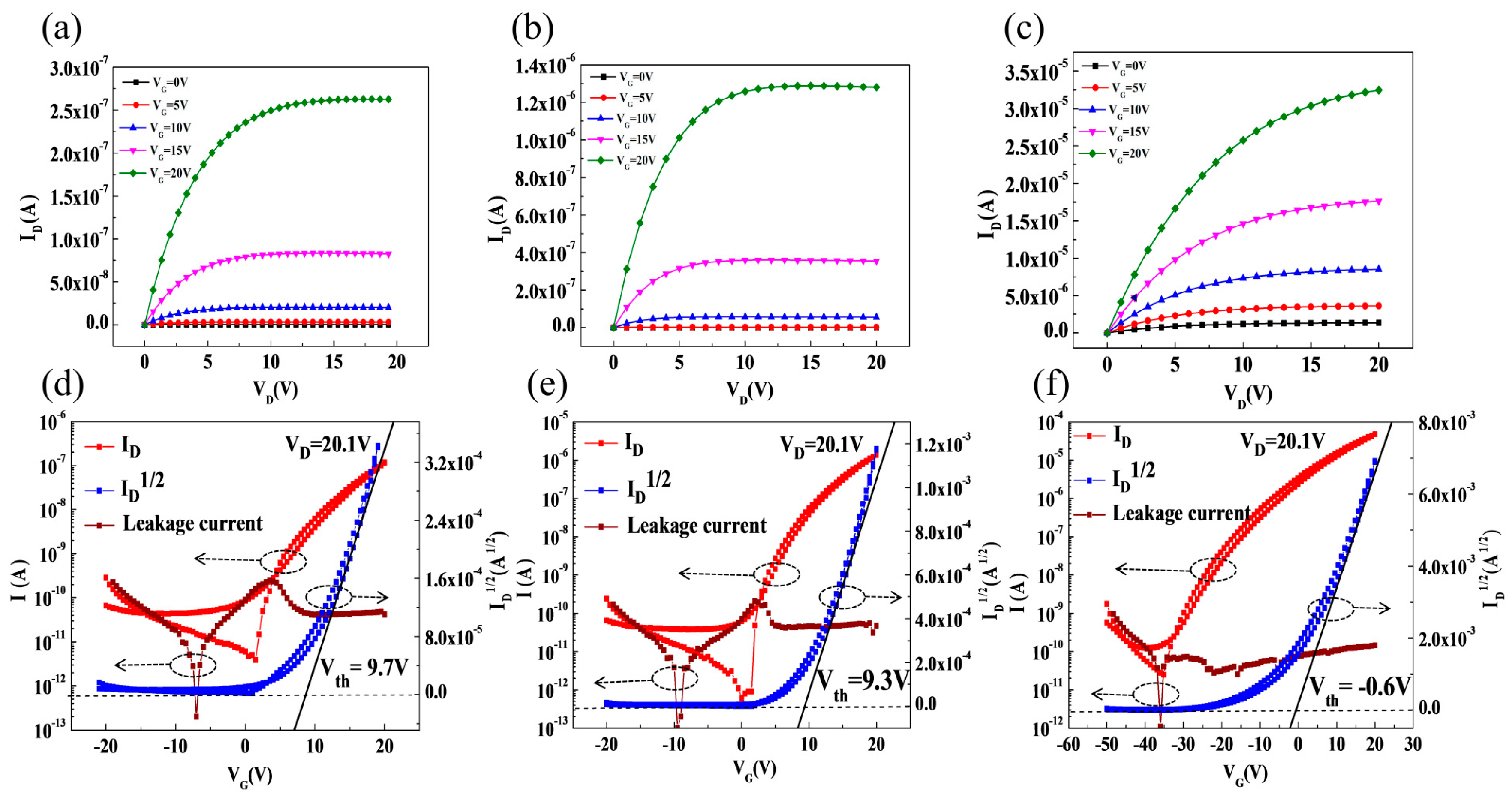
| Device | Ion/Ioff | SS (V/Decade) | μsat (cm2/V·s) | Vth (V) |
|---|---|---|---|---|
| S1 | 3.02 × 10⁴ | 0.86 | 0.04 | 9.7 |
| S2 | 7.47 × 10⁴ | 1.53 | 0.50 | 9.3 |
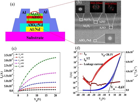
| S3 | 1.92 × 10⁶ | 2.34 | 2.47 | −0.6 |
© 2017 by the authors. Licensee MDPI, Basel, Switzerland. This article is an open access article distributed under the terms and conditions of the Creative Commons Attribution (CC BY) license ( http://creativecommons.org/licenses/by/4.0/).
Share and Cite
Yao, R.; Zheng, Z.; Zeng, Y.; Liu, X.; Ning, H.; Hu, S.; Tao, R.; Chen, J.; Cai, W.; Xu, M.; et al. All-Aluminum Thin Film Transistor Fabrication at Room Temperature. Materials 2017, 10, 222. https://doi.org/10.3390/ma10030222
Yao R, Zheng Z, Zeng Y, Liu X, Ning H, Hu S, Tao R, Chen J, Cai W, Xu M, et al. All-Aluminum Thin Film Transistor Fabrication at Room Temperature. Materials. 2017; 10(3):222. https://doi.org/10.3390/ma10030222
Chicago/Turabian StyleYao, Rihui, Zeke Zheng, Yong Zeng, Xianzhe Liu, Honglong Ning, Shiben Hu, Ruiqiang Tao, Jianqiu Chen, Wei Cai, Miao Xu, and et al. 2017. "All-Aluminum Thin Film Transistor Fabrication at Room Temperature" Materials 10, no. 3: 222. https://doi.org/10.3390/ma10030222