Article

Amorphous InGaMgO Ultraviolet Photo-TFT with Ultrahigh Photosensitivity and Extremely Large Responsivity

1
School of Microelectronics and Solid-State Electronics, University of Electronic Science and Technology of China, Chengdu 610054, China
2
State Key Laboratory of Electronic Thin Films and Integrated Devices, Chengdu 610054, China
*
Authors to whom correspondence should be addressed.
Materials 2017, 10(2), 168; https://doi.org/10.3390/ma10020168
Submission received: 28 December 2016 / Revised: 30 January 2017 / Accepted: 9 February 2017 / Published: 13 February 2017
(This article belongs to the Special Issue Oxide Semiconductor Thin-Film Transistor)

Abstract

:
Recently, amorphous InGaZnO ultraviolet photo thin-film transistors have exhibited great potential for application in future display technologies. Nevertheless, the transmittance of amorphous InGaZnO (~80%) is still not high enough, resulting in the relatively large sacrifice of aperture ratio for each sensor pixel. In this work, the ultraviolet photo thin-film transistor based on amorphous InGaMgO, which processes a larger bandgap and higher transmission compared to amorphous InGaZnO, was proposed and investigated. Furthermore, the effects of post-deposition annealing in oxygen on both the material and ultraviolet detection characteristics of amorphous InGaMgO were also comprehensively studied. It was found that oxygen post-deposition annealing can effectively reduce oxygen vacancies, leading to an optimized device performance, including lower dark current, higher sensitivity, and larger responsivity. We attributed it to the combined effect of the reduction in donor states and recombination centers, both of which are related to oxygen vacancies. As a result, the 240-min annealed device exhibited the lowest dark current of 1.7 × 10⁻¹⁰ A, the highest photosensitivity of 3.9 × 10⁶, and the largest responsivity of 1.5 × 10⁴ A/W. Therefore, our findings have revealed that amorphous InGaMgO photo thin-film transistors are a very promising alternative for UV detection, especially for application in touch-free interactive displays.

1. Introduction

The amorphous oxide semiconductors based thin film transistors (TFTs), represented by amorphous InGaZnO (a-IGZO) TFTs, have been intensively developed for a variety of applications in flat panel displays (FPDs), including electronic papers (e-papers), organic light-emitting-diode displays (OLEDs), and liquid crystal displays (LCDs) [1,2,3]. In addition, a-IGZO TFTs have also been demonstrated to act as ultraviolet (UV) photo thin-film transistors (photo-TFTs) employed in an active matrix, accordingly realizing the contact-free interactive display [4]. For example, Tze-Ching Fung et al. studied both the wavelength and intensity dependent photo-responses in a-IGZO photo-TFTs, suggesting the possibility of using a-IGZO TFT as UV-light photo-sensor/imager [5]; Hsiao-Wen Zan et al. fabricated an a-IGZO visible-light photo-TFT by employing a polymeric light absorption capping layer [6]; and T. H. Chang et al. improved a-IGZO photo-TFTs by optimizing the oxygen partial pressures during the deposition, resulting in a high responsivity (R) over 4.75 A/W [7]. Compared to conventional two-terminal photoconductors, a-IGZO photo-TFTs usually have a much higher photosensitivity (P) by selecting the operation voltage appropriately, leading to enhanced sensitivity to the irradiation [8]. However, due to the relatively low visible transmittance of a-IGZO thin films, the introduction of a-IGZO photo-TFTs will result in the sacrifice of aperture ratio. To solve this problem, most researchers have attempted to increase the field-effect mobility (μFE) of a-IGZO TFTs and thus reduce the switch size. L. X. Qian et al. treated the a-IGZO TFT with HaLaO gate dielectric in a CHF3/O2 plasma, and thus increased its μFE to an ultrahigh value of 39.8 cm2/Vs [3]. Moreover, G. M. Wu et al. proposed a-IGZO TFTs with a μFE of 33.5 cm2/Vs by using atmospheric pressure plasma treatment on e-beam deposited silicon dioxide gate dielectric layers [9]. Very recently, L.L. Zheng et al. fabricated a high-mobility a-IGZO TFT (μFE > 60 cm2/Vs) with an atomic-layer-deposited SiO2 gate insulator [10]. Nevertheless, it is still quite difficult to realize the μFE of a-IGZO TFTs over 70 cm2·v−1·s−1 so far. Recently, it was reported that the incorporation of light main-group metals—for example, Al, Mg and Ca—in oxide semiconductors could lead to improved optical transmission and enlarged bandgap (Eg) [11]. For instance, ZnMgO (3.68 eV) presents a larger Eg than ZnO (3.37 eV), and so can act like a barrier layer to build up ZnMgO/ZnO heterojunction and realize a high-electron-mobility transistor (HEMT) [12,13]. In this work, we tried to increase aperture ratio by enlarging the transmittance of photo-TFTs for each sensor pixel. Accordingly, the photo-TFT based on InGaMgO (IGMO) film, in which Zn was completely replaced by Mg, was firstly proposed, and its UV photodetection characteristics were comprehensively investigated. Moreover, the post-deposition annealing (PDA) in ambient oxygen was conducted to further optimize film quality and device performance. It was found that the density of oxygen vacancies (Ovac) in IGMO film was effectively reduced with the PDA treatment, leading to the decrease of dark current (Idark) and the increase of photo current (Iphoto). As a result, the UV photodetection characteristics of IGMO photo-TFT—including P, R, and internal gain (G)—were dramatically improved.

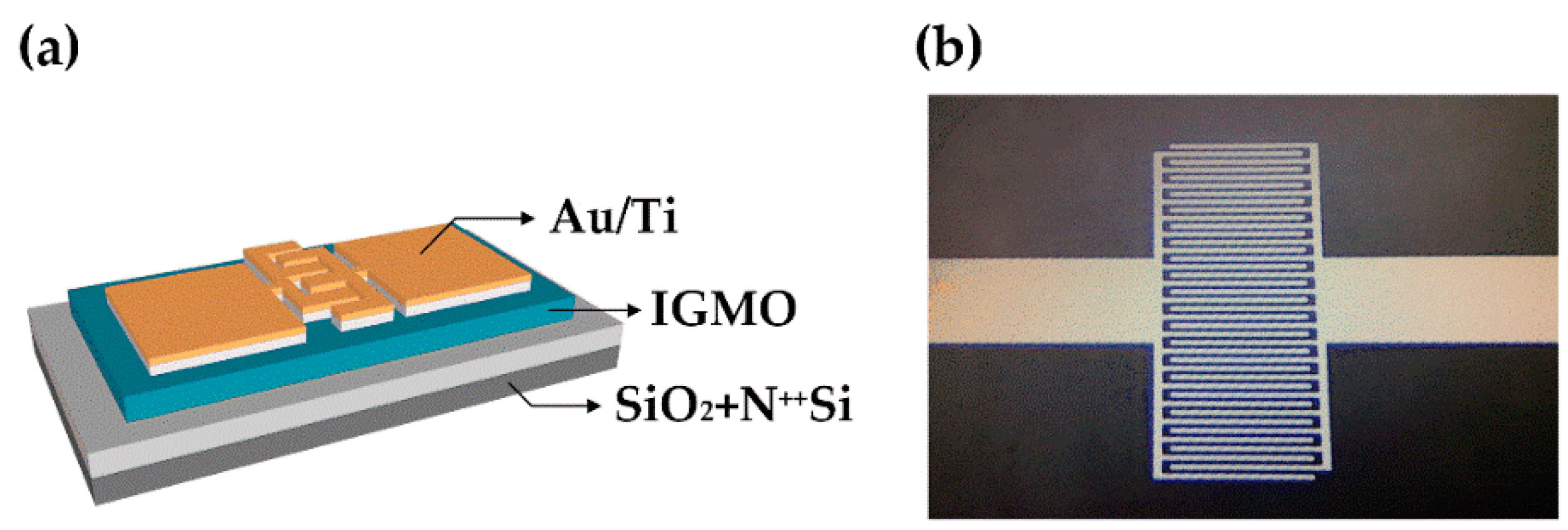
2. Experimental Details

The schematic and typical optical microscope image of IGMO photo-TFTs are shown in Figure 1a,b, respectively. Firstly, n-type (100) heavy-doped Si substrates (0.01 Ω·cm) with a 100-nm thermal grown SiO2 dielectric film at the top were cleaned by the conventional Radio Corporation of America (RCA) method. Secondly, IGMO films were synthesized on each sample by plasma-assisted molecular beam epitaxy (MBE) at room temperature. In order to compare with a-IGZO (In: Ga:Zn = 2:2:1) fairly, the composition of a-IGMO film was maintained at In: Ga:Mg = 2:2:1 [14]. During the synthesis, the background vacuum in the growth chamber was about 3 × 10⁻⁸ torr, the RF power of O2 plasma was fixed at 300 W, and the O2 flow rate was fixed at 2 sccm by a mass flow controller. Thirdly, considering the ultra-high vacuum demanded in MBE chamber, the flow rate of O2 must be lower than 4 sccm, which is far from enough for the optimization of the oxygen contents in a-IGMO films, even with the assistance of RF plasma. Therefore, the O2 PDA treatments at 350 °C in the furnace were conducted at different time periods (0, 120, and 240 min). The PDA treatment was employed at the atmospheric pressure with a fixed O2 flow rate of 1.2 × 10³ sccm. Finally, the conventional lift-off process was utilized to form the interdigital source/drain electrodes, which consisted of 30-nm Ti and 50-nm Au deposited by e-beam evaporator. The width, length, and spacing of the electrode fingers were 12.5, 500, and 12.5 μm, respectively.
As for the material properties, the crystallinities, thicknesses, transmittance spectra, and binding energies of the IGMO films were investigated by Bede D1 multi-functional X-ray diffraction (XRD), Veeco Dektak 150 surface profiler, ultraviolet spectrophotometer PERSEE TU-1810, and XSAM800 X-ray photoelectron spectroscopy (XPS), respectively. In addition, the current-voltage (I–V) characteristics of IGMO photo-TFTs were measured by an Agilent 4155B semiconductor parameter analyzer. Lighting emitting diode (LED) lamps with different wavelengths were employed as the light sources during the photosensitivity evaluation.

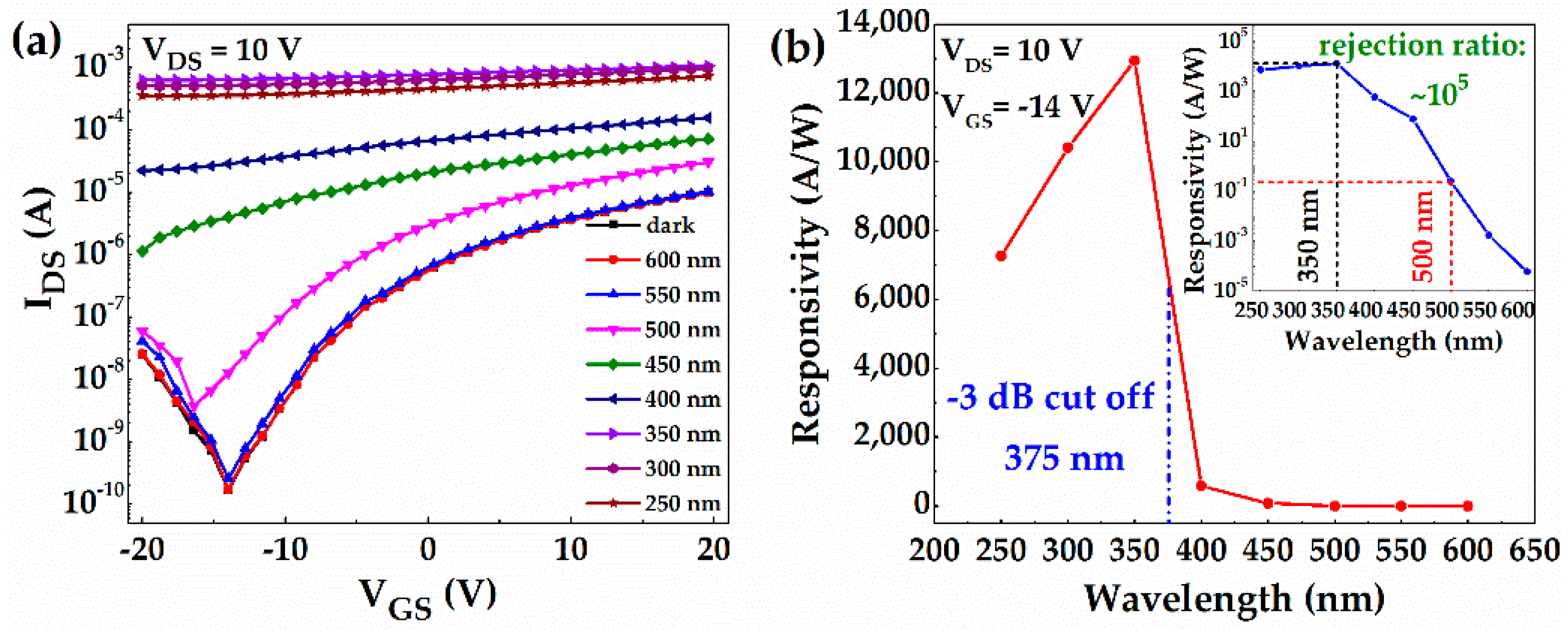
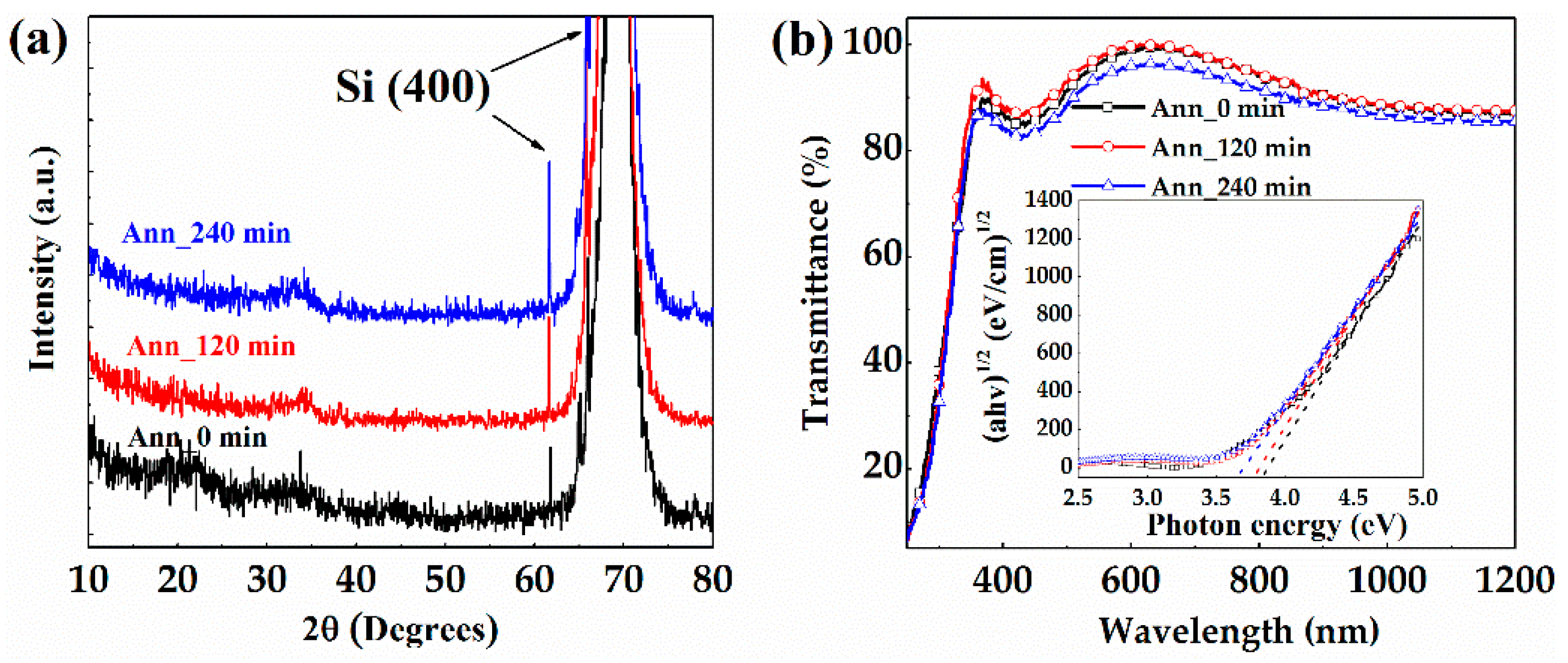
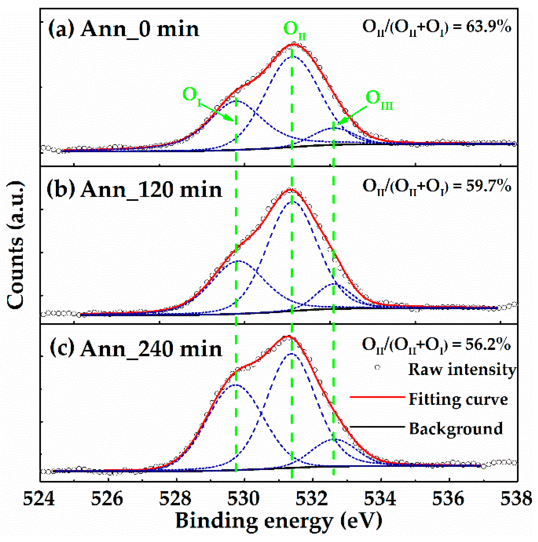
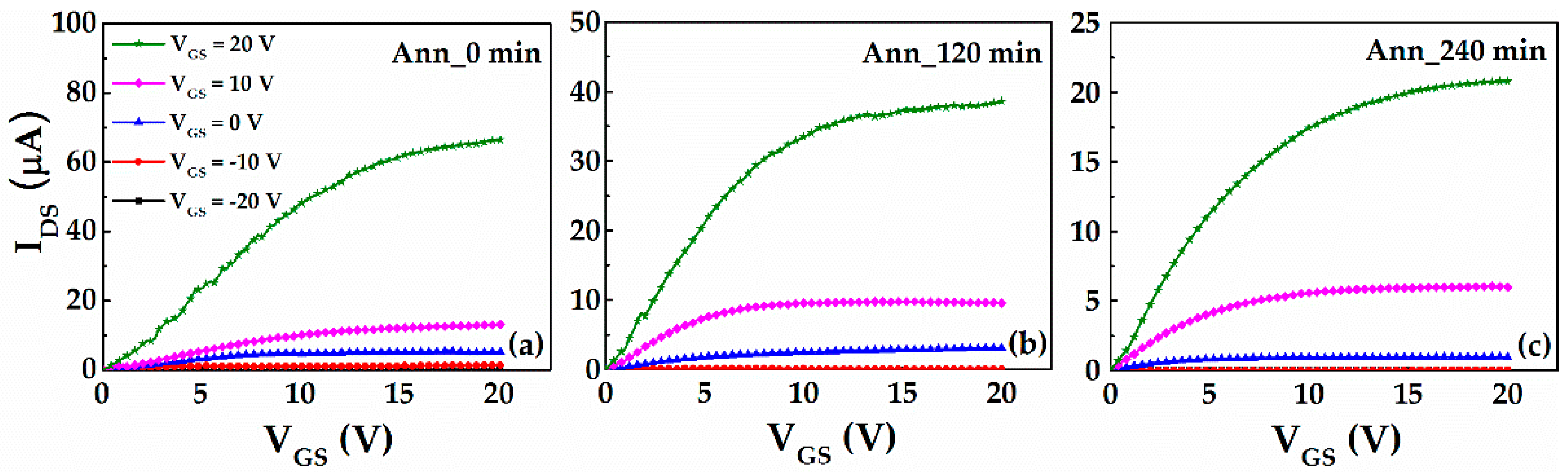
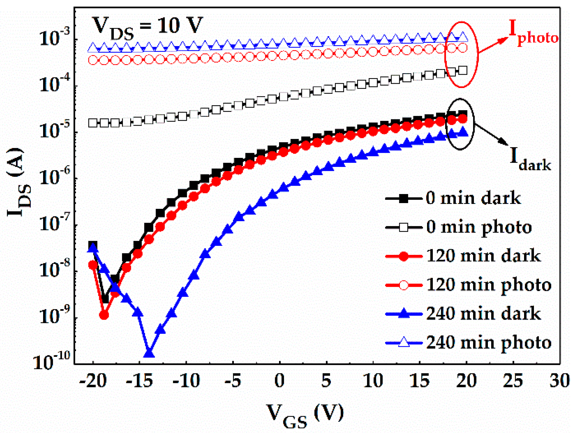
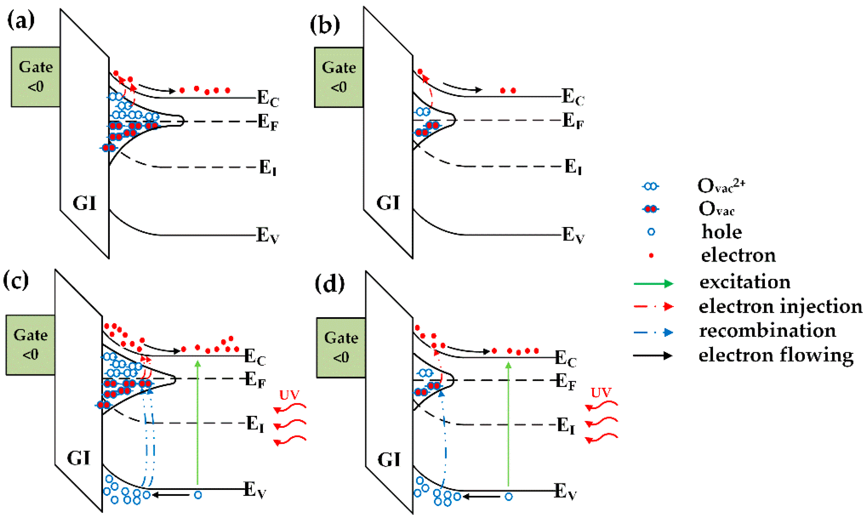
3. Results and Discussion

Figure 2a shows the XRD spectra of the IGMO films with different PDA time. For each sample, there is no evident peak except the (400) diffraction peak of Si substrate [15], implying that all samples remain in the amorphous phase even after the PDA treatment. This can be attributed to the room temperature deposition and relatively low PDA temperature of 350 °C. Furthermore, the transmittance spectra of a-IGMO films grown on vitreous quartz substrate were measured as shown in Figure 2b. All the samples exhibited high transmittances of approximately 90% in visible spectra, clearly larger than the previously-reported a-IGZO films, whose visible spectral transmittances are approximately 80% [16,17,18]. This has demonstrated the possibility of our proposed a-IGMO photo-TFTs for enlarging the aperture ratio of the sensor pixel. Furthermore, the Eg of a-IGMO films were extracted based on Tauc’s law as listed below [19]:
( α h υ ) 1 / 2 = A ( h υ E g )
where α is the absorption coefficient, is the incident photon energy, and A is a constant. In general, α can be expressed by the Equation [20]:
α = 1 t ln ( 1 T )
where t is the thickness of a-IGMO film, and T is its transmittance. The thicknesses of the 0-, 120-, and 240-min annealed a-IGMO films were 54.2, 49.4, and 48.3 nm, respectively. As shown in the inset of Figure 1b, Eg’s were determined to be 3.81, 3.78, and 3.62 eV for the 0-, 120-, and 240-min annealed a-IGMO films, respectively. Note that, all the values are larger than that of a-IGZO films (~3.1 eV) [21]. We attribute the monotonically decreasing Eg of a-IGMO films with prolonging PDA time to the Burstein-Moss (BM) effect [22,23]. It was reported that Eg can be enlarged with the increase of carrier concentration due to the occupation of the states near conduction band minimum (CBM) and accordingly the blue-shift of the optical absorption edge. According to XPS analysis, the percentage of oxygen atoms in the 0-, 120-, and 240-min annealed a-IGMO films are 41.3%, 45.4% and 52.7%, respectively (much lower than the stoichiometric ratio of 58.3%), suggesting our prepared a-IGMO films are all highly oxygen deficient. Usually, oxygen vacancies act as donor states in n-type metal oxide semiconductors and release electrons [24]. In our case, with the PDA treatment, the conduction band states near CBM in a-IGMO film become unoccupied due to the reduction of electron concentration, thus resulting in the narrowing of Eg.
The electrical properties of a-IGMO films were extracted from the results of Hall-effect measurement, and listed in Table 1. It reveals that the electrical resistivity of a-IGMO films increase monotonically when prolonging the PDA periods, due to the decrease of both electron concentration (Ne) and Hall mobility (μHall). It is attributed to the reduction of Ovac by PDA treatment in oxygen. Figure 3 exhibits the XPS spectra of O 1s core level for a-IGMO films with different PDA time. The binding energies have been calibrated according to the reference of C 1 s at 284.8 eV [25]. All the O 1s peaks were analyzed through Lorentzian-Gaussian fitting, and separated into those centered at (1) ~529.7 eV (OI), which represents the metal-oxygen bonds (M-O) without Ovac; (2) ~531.4 eV (OII), which represents the M-O in oxygen deficient regions; and (3) ~532.6 eV (OIII), which represents the loose oxygen bonds on the surface related to hydroxide (O-H) [26]. Accordingly, the atomic ratios of OII/(OII+OI) are 63.9%, 59.7%, and 56.2% for the 0-, 120-, and 240-min annealed a-IGMO films, respectively. Clearly, the as-deposited a-IGMO film has the highest density of Ovac within all the samples, and the Ovacs were effectively suppressed with the prolonging of PDA time which further confirmed the results of Hall-effect measurement.
As shown in Figure 4, the output characteristics of a-IGMO photo-TFTs with different PDA time were measured in dark. All the devices exhibit typical n-type TFT output characteristics with distinct linear and saturation regions. Figure 5 shows the transfer characteristics of a-IGMO photo-TFTs, which were measured under a drain-to-source voltage (VDS) of 10 V in dark and under 350-nm radiation, respectively. It was found that Idark was decreased about one order of magnitude with prolonging the O2 annealing time from 0 to 240 min, as shown in Figure 5. It can be attributed to the reduction of Ovacs, which act as shallow donor states (Figure 6a,b), as revealed by the previously discussed XPS result. Furthermore, the subthreshold swing (SS) and the trap density at/near the semiconductor/dielectric interface (Nit), was determined according to the equations [27]:
S S = [ log ( I D S ) V G S ] 1
N i t = [ S S log ( e ) k T / q 1 ] C O X q
where k is the Boltzmann constant, T is absolute temperature, COX is the gate-oxide capacitance per unit area, and q is the electronic charge. Accordingly, the SS were 0.87, 0.69, and 0.48 V/dec, while the Nit were calculated to be 8.01 × 10¹¹, 6.24 × 10¹¹, and 4.16 × 1011 cm−3 for 0-, 120-, and 240-min annealed a-IGMO photo-TFTs, respectively. It was revealed that both SS and Nit decreases as the PDA time rises from 0 to 240 min, partly demonstrating the effect of PDA treatment in oxygen on the suppression of defects.
When the devices were illuminated by a 350-nm and 25-μW/cm2 UV light, Iphoto was significantly increased with the prolonging of the PDA time from 0 to 240 min. According to previous reports, Iphoto in photo-TFTs might be reduced by the decrease of Ovac-related defects due to the suppression of photoconductive internal gain, which is contrary to our result [28]. In fact, Ovacs can also form deep states in the forbidden gap, which often act as effective recombination centers of photogenerated carriers as illustrated in Figure 6c,d [29]. Hence, we suggest the observed increase of Iphoto should be ascribed to the reduction of recombination centers with the PDA treatment in oxygen. Note that, in the 120-min annealed sample, the suppression effect of O2 annealing on Ovacs might be more obvious for the deep states due to their larger density. Consequently, it led to the different levels of impact on photo and dark currents. When the annealing time prolonged to 240 min, both deep and shallow Ovac-related states were intensively reduced simultaneously, resulting in the significant change in both photo and dark currents. To further evaluate the photodetection properties of a-IGMO photo-TFTs, the P, R, and G were also determined according to the following equations [30]:
P = s i g n a l n o i s e = I p h o t o I d a r k
R = I p h o t o I d a r k P o p t
G = I p h o t o I d a r k q η ( h ν P o p t )
where η is the quantum efficiency, and Popt is the incident light power. Here, η is assumed to be equal to 1, which means that an incident photon generated one pair of electron and hole [31]. In order to compare their best photodetection characteristics, different VGSs, which correspond to the lowest dark current for each sample, were selected. Accordingly, P’s were determined to be 6.3 × 10³, 3.1 × 10⁵, and 3.9 × 10⁶ for 0-, 120-, and 240-min annealed samples, respectively. Clearly, P of a-IGMO photo-TFTs was significantly improved by prolonging the PDA time. Similarly, both R and G were increased with a longer PDA treatment time, and listed in Table 1. In addition, there are extremely high Gs in our proposed devices, which is attributed to the holes trapping by Ovac-related defects. As a result, the 240-min annealed a-IGMO photo-TFTs exhibits the best device performance, including the lowest Idark of 1.7 × 10⁻¹⁰ A, the largest P of 3.9 × 10⁶, and the highest R of 1.5 × 10⁴ A/W. All the parameters are listed in Table 1 for comparison. However, the turn-on voltages (Vons) are too negative as shown in Figure 5, and the further optimization might be required in the future work, for example, by prolonging the O2 annealing time, increasing the O2 flow rate, or raising the annealing temperature.
Figure 7a reveals the λ-dependence of the 240-min annealed photo-TFT, which was measured by exposing them to 600-, 550-, 500-, 450-, 400-, 350-, 300-, and 250-nm lights with the fixed power of 25 μW/cm2. Under UV illumination, IDS increased significantly, which can be attributed to the generation of non-equilibrium carriers [32]. Moreover, the shorter the light wavelength, the more obvious the increase of IDS. In particular, the a-IGMO photo-TFT cannot be effectively modulated by VGS once upon the UV illuminations (λ < 400 nm). Moreover, threshold voltage (VTH), which was extracted from the equation [1]:
I D S 1 / 2 = W 2 L μ F E C O X ( V G S V T H )
negatively shifted in the 240-min annealed a-IGMO photo-TFT with the reduction of illumination light wavelength, which further confirmed the increase of photogenerated carriers. In addition, the spectral response characteristics of the 240-min annealed a-IGMO photo-TFT at VGS of –14 V and VDS of 10 V is exhibited in Figure 7b, in which the inset shows the plot in logarithmic scales. It is clear that the a-IGMO photo-TFT is only sensitive to illumination with a λ less than 450 nm. The peak response occurs at ~350 nm, and the −3 dB cutoff wavelength is ~375 nm, which indicates our proposed device is a true UV photodetector. According to the determined bandgap (3.62 eV), the intrinsic-absorption wavelength can be calculated to be ~340 nm. In contrast, the −3 dB cutoff wavelength is generally larger than the intrinsic-absorption one due to the transition from tail-states and other sub-bandgap defect states to the conduction band [33]. Moreover, the UV-to-visible rejection ratio, which is defined as the ratio of R at 350 and 500 nm [34], is about five orders of magnitude, proving the high sensitivity of our device. The observed decrease of R when the λ is less than 350 nm might be attributed to the exciton-exciton annihilation—i.e., the interaction of excitons with each other when their density is dramatically enhanced by high-energy photons [30]. As seen in Table 2, the 240-min annealed a-IGMO photo-TFT is compared with various previously reported a-IGZO UV photodetectors. Clearly, our fabricated device exhibits an extremely high performance in the key parameters.

4. Conclusions

In conclusion, the photo-TFT based on a-IGMO thin film has been proposed and fabricated, and a-IGMO exhibits larger bandgap and higher visible transmittance in comparison to a-IGZO. Moreover, the XPS results reveal that the PDA treatment in oxygen can effectively suppress the density of Ovacs in a-IGMO film, thus significantly reducing the Idark, SS, and Nit of the photo-TFT. Furthermore, a dramatically increased Iphoto was observed, which may be attributed to the reduction of recombination centers related to Ovacs. As a result, a continuous improvement in P, R, and η was exhibited by prolonging the PDA time from 0 to 240 min, and the 240-min annealed sample exhibited the lowest Idark of 1.7 × 10⁻¹⁰ A, the highest P of 3.9 × 10⁶, and the largest R of 1.5 × 10⁴ A/W to 350-nm UV radiation, exhibiting more outstanding performance compared to many previously-reported amorphous UV photodetectors. In summary, this work has demonstrated that a-IGMO photo-TFT is a promising alternative for UV photodetection, especially for application in transparent contact-free interactive displays.

Acknowledgments

This work was supported by the National Natural Science Foundation of China under contract 61504022 and the Fundamental Research Funds for the Central Universities under grant No. ZYGX2015KYQD010.

Author Contributions

Yiyu Zhang, Ling-Xuan Qian, and Xingzhao Liu conceived and designed the experiments; Yiyu Zhang and Zehan Wu performed the experiments; Yiyu Zhang and Ling-Xuan Qian analyzed the data; Ling-Xuan Qian and Xingzhao Liu contributed materials/analysis tools; Yiyu Zhang and Ling-Xuan Qian wrote the paper.

Conflicts of Interest

The authors declare no conflicts of interest.

References

  1. Kamiya, T.; Nomura, K.; Hosono, H. Present status of amorphous In-Ga-Zn-O thin-film transistors. Sci. Technol. Adv. Mater. 2010, 11, 044305. [Google Scholar] [CrossRef] [PubMed]
  2. Qian, L.X.; Lai, P.T.; Tang, W.M. Effects of Ta incorporation in La2O3 gate dielectric of InGaZnO thin-film transistor. Appl. Phys. Lett. 2014, 104, 123505. [Google Scholar] [CrossRef] [Green Version]
  3. Qian, L.X.; Lai, P.T. Fluorinated InGaZnO Thin-Film Transistor With HfLaO Gate Dielectric. IEEE Electron Device Lett. 2014, 35, 363–365. [Google Scholar] [CrossRef]
  4. Jeon, S.; Ahn, S.E.; Song, I.; Kim, C.J.; Chung, U.I.; Lee, E.; Yoo, I.; Nathan, A.; Lee, S.; Robertson, J.; et al. Gated three-terminal device architecture to eliminate persistent photoconductivity in oxide semiconductor photosensor arrays. Nat. Mater. 2012, 11, 301–305. [Google Scholar] [CrossRef] [PubMed]
  5. Fung, T.C.; Chuang, C.S.; Nomura, K.; Shieh, H.P.D.; Hosono, H.; Kanicki, J. Photofield-Effect in Amorphous In-Ga-Zn-O (a-IGZO) Thin-Film Transistors. J. Inf. Display 2008, 9, 21–29. [Google Scholar] [CrossRef]
  6. Zan, H.-W.; Chen, W.-T.; Hsueh, H.-W.; Kao, S.-C.; Ku, M.-C.; Tsai, C.-C.; Meng, H.-F. Amorphous indium-gallium-zinc-oxide visible-light phototransistor with a polymeric light absorption layer. Appl. Phys. Lett. 2010, 97, 203506. [Google Scholar] [CrossRef]
  7. Chang, T.H.; Chiu, C.J.; Weng, W.Y.; Chang, S.J.; Tsai, T.Y.; Huang, Z.D. High responsivity of amorphous indium gallium zinc oxide phototransistor with Ta2O5 gate dielectric. Appl. Phys. Lett. 2012, 101, 261112. [Google Scholar] [CrossRef]
  8. Pei, Z.; Lai, H.-C.; Wang, J.-Y.; Chiang, W.-H.; Chen, C.-H. High-Responsivity and High-Sensitivity Graphene Dots/a-IGZO Thin-Film Phototransistor. IEEE Electron Device Lett. 2015, 36, 44–46. [Google Scholar] [CrossRef]
  9. Wu, G.M.; Sahoo, A.K.; Lin, J.Y. Effects of e-beam deposited gate dilelctric layers with atmospheric pressure plasma treatment for IGZO thin-film transistors. Surf. Coat. Technol. 2016, 306, 151–158. [Google Scholar] [CrossRef]
  10. Zheng, L.-L.; Ma, Q.; Wang, Y.-H.; Liu, W.-J.; Ding, S.-J.; Zhang, D.W. High-performance unannealed a-InGaZnO TFT with an atomic-layer-deposited SiO2 insulator. IEEE Electron Device Lett. 2016, 37, 743–746. [Google Scholar] [CrossRef]
  11. Murat, A.; Medvedeva, J.E. Electronic properties of layered multicomponent wide-band-gap oxides: A combinatorial approach. Phys. Rev. B 2012, 85, 13. [Google Scholar] [CrossRef]
  12. Chen, H.; Gu, S.; Liu, J.; Ye, J.; Tang, K.; Zhu, S.; Zheng, Y. Two-dimensional electron gas related emissions in ZnMgO/ZnO heterostructures. Appl. Phys. Lett. 2011, 99, 211906. [Google Scholar] [CrossRef]
  13. Begum, K.R.; Kolvekar, S.B.; Sankeshwar, N.S. Electron mobility in MgZnO/ZnO heterojunctions. AIP Conf. Proc. 2013, 1536, 447–448. [Google Scholar]
  14. Park, J.S.; Maeng, W.J.; Kim, H.S.; Park, J.S. Review of recent developments in amorphous oxide semiconductor thin-film transistor devices. Thin Solid Films 2012, 520, 1679–1693. [Google Scholar] [CrossRef]
  15. Samsudin, M.E.A.; Zainal, N.; Hassan, Z. Deposition of a polycrystalline GaN layer on a porous Si/Si substrate by an electron beam evaporator with a successive ammonia annealing treatment. J. Alloys Compd. 2017, 690, 397–402. [Google Scholar] [CrossRef]
  16. Kim, E.; Jang, W.J.; Kim, W.; Park, J.; Lee, M.K.; Park, S.H.K.; Choi, K.C. Suppressed Instability of a-IGZO Thin-Film Transistors Under Negative Bias Illumination Stress Using the Distributed Bragg Reflectors. IEEE Trans. Electron Devices 2016, 63, 1066–1071. [Google Scholar] [CrossRef]
  17. Chen, M.C.; Chang, T.C.; Huang, S.Y.; Chen, S.C.; Hu, C.W.; Tsai, C.T.; Sze, S.M. Bipolar Resistive Switching Characteristics of Transparent Indium Gallium Zinc Oxide Resistive Random Access Memory. Electrochem. Solid-State Lett. 2010, 13, II191–II193. [Google Scholar] [CrossRef]
  18. Yoshidomi, S.; Kimura, S.; Hasumi, M.; Sameshima, T. Indium-gallium-zinc-oxide layer used to increase light transmittance efficiency of adhesive layer for stacked-type multijunction solar cells. Jpn. J. Appl. Phys. 2015, 54, 5. [Google Scholar] [CrossRef]
  19. Leenheer, A.J.; Perkins, J.D.; van Hest, M.; Berry, J.J.; O‘Hayre, R.P.; Ginley, D.S. General mobility and carrier concentration relationship in transparent amorphous indium zinc oxide films. Phys. Rev. B 2008, 77, 5. [Google Scholar] [CrossRef]
  20. Xue, S.W.; Zu, X.T.; Zhou, W.L.; Deng, H.; Xiang, X.; Zhang, L. Effects of post-thermal annealing on the optical constants of ZnO thin film. J. Alloys Compd. 2008, 448, 21–26. [Google Scholar] [CrossRef]
  21. Hays, D.C.; Gila, B.P.; Pearton, S.J.; Ren, F. ZrSiOx/IGZO heterojunctions band offsets determined by X-ray photoelectron spectroscopy. Vacuum 2015, 122, 195–200. [Google Scholar] [CrossRef]
  22. Liu, X.; Zhang, Q.; Yip, J.N.; Xiong, Q.; Sum, T.C. Wavelength Tunable Single Nanowire Lasers Based on Surface Plasmon Polariton Enhanced Burstein-Moss Effect. Nano Lett. 2013, 13, 5336–5343. [Google Scholar] [CrossRef] [PubMed]
  23. Lim, K.H.; Kim, K.; Kim, S.; Park, S.Y.; Kim, H.; Kim, Y.S. UV-visible spectroscopic analysis of electrical properties in alkali metal-doped amorphous zinc tin oxide thin-film transistors. Adv. Mater. 2013, 25, 2994–3000. [Google Scholar] [CrossRef] [PubMed]
  24. Xiao, X.; Deng, W.; Chi, S.P.; Shao, Y.; He, X.; Wang, L.Y.; Zhang, S.D. Effect of O2 Flow Rate During Channel Layer Deposition on Negative Gate Bias Stress-Induced Vth Shift of a-IGZO TFTs. IEEE Trans. Electron Devices 2013, 60, 4159–4164. [Google Scholar] [CrossRef]
  25. Yao, J.; Zhang, S.; Gong, L. Band offsets in ZrO2/InGaZnO4 heterojunction. Appl. Phys. Lett. 2012, 101, 093508. [Google Scholar] [CrossRef]
  26. Seo, S.-J.; Hwang, Y.H.; Bae, B.-S. Postannealing Process for Low Temperature Processed Sol–Gel Zinc Tin Oxide Thin Film Transistors. Electrochem. Solid-State Lett. 2010, 13, H357. [Google Scholar] [CrossRef]
  27. Ji, K.H.; Kim, J.I.; Mo, Y.G.; Jeong, J.H.; Yang, S.; Hwang, C.S.; Park, S.H.K.; Ryu, M.K.; Lee, S.Y.; Jeong, J.K. Comparative Study on Light-Induced Bias Stress Instability of IGZO Transistors With SiNx and SiO2 Gate Dielectrics. IEEE Electron Device Lett. 2010, 31, 1404–1406. [Google Scholar] [CrossRef]
  28. Soci, C.; Zhang, A.; Xiang, B.; Dayeh, S.A.; Aplin, D.P.R.; Park, J.; Bao, X.Y.; Lo, Y.H.; Wang, D. ZnO nanowire UV photodetectors with high internal gain. Nano Lett. 2007, 7, 1003–1009. [Google Scholar] [CrossRef] [PubMed]
  29. Guo, D.; Wu, Z.; Li, P.; An, Y.; Liu, H.; Guo, X.; Yan, H.; Wang, G.; Sun, C.; Li, L.; et al. Fabrication of β-Ga2O3 thin films and solar-blind photodetectors by laser MBE technology. Opt. Mater. Express 2014, 4, 1067. [Google Scholar] [CrossRef]
  30. Hamilton, M.C.; Martin, S.; Kanicki, J. Thin-film organic polymer phototransistors. IEEE Trans. Electron Devices 2004, 51, 877–885. [Google Scholar] [CrossRef]
  31. Tabares, G.; Hierro, A.; Ulloa, J.M.; Guzman, A.; Munoz, E.; Nakamura, A.; Hayashi, T.; Temmyo, J. High responsivity and internal gain mechanisms in Au-ZnMgO Schottky photodiodes. Appl. Phys. Lett. 2010, 96. [Google Scholar] [CrossRef]
  32. Park, S.; Park, S.; Ahn, S.-E.; Song, I.; Chae, W.; Han, M.; Lee, J.; Jeon, S. Effects of operational and geometrical conditions upon photosensitivity of amorphous InZnO thin film transistors. J. Vac. Sci. Technol. B 2013, 31, 050605. [Google Scholar] [CrossRef]
  33. Pankove, J.I. Optical Processes in Semiconductors; Dover Pubilcations, Inc.: New York, NY, USA, 1971; pp. 43, 62. [Google Scholar]
  34. Jiang, D.-Y.; Zhang, X.-Y.; Liu, Q.-S.; Bai, Z.-H.; Lu, L.-P.; Wang, X.-C.; Mi, X.-Y.; Wang, N.-L.; Shen, D.-Z. Improved ultraviolet/visible rejection ratio using MgZnO/SiO2/n-Si heterojunction photodetectors. Appl. Surf. Sci. 2010, 256, 6153–6156. [Google Scholar] [CrossRef]
  35. Chen, W.-T.; Zan, H.-W. High-performance light-erasable memory and real-time ultraviolet detector based on unannealed Indium-Gallium-Zinc-Oxide thin-film transistor. IEEE Electron Device Lett. 2012, 33, 77–79. [Google Scholar] [CrossRef]
  36. Jiang, D.L.; Li, L.; Chen, H.Y.; Gao, H.; Qiao, Q.; Xu, Z.K.; Jiao, S.J. Realization of unbiased photoresponse in amorphous InGaZnO ultraviolet detector via a hole-trapping process. Appl. Phys. Lett. 2015, 106, 171103. [Google Scholar] [CrossRef]
  37. Zhou, H.T.; Li, L.; Chen, H.Y.; Guo, Z.; Jiao, S.J.; Sun, W.J. Realization of a fast-resoponse flexible ultraviolet photodetector employing a metal-semiconductor-metal structure InGaZnO photodiode. RSC Adv. 2015, 5, 87993. [Google Scholar] [CrossRef]
Figure 1. (a) Schematic and (b) optical microscope image of IGMO photo-TFT.
Materials 10 00168 g001
Figure 2. (a) XRD spectra of 0-, 120-, and 240-min annealed IGMO films; (b) transmittance spectra of a-IGMO films, the inset was the plots of (αhν)1/2 vs. .
Materials 10 00168 g002
Figure 3. O 1 s XPS spectra of (a) 0-min; (b) 120-min; and (c) 240-min annealed a-IGMO films.
Materials 10 00168 g003
Figure 4. Output characteristics of (a) 0-min; (b) 120-min; and (c) 240-min annealed a-IGMO photo-TFTs.
Materials 10 00168 g004
Figure 5. Transfer characteristics of a-IGMO photo-TFTs in dark and under 350-nm UV radiation.
Materials 10 00168 g005
Figure 6. Energy band diagram of: (a) as-deposited a-IGMO photo-TFT in dark; (b) annealed a-IGMO photo-TFT in dark; (c) as-deposited a-IGMO photo-TFT under 350-nm UV illumination, and (d) annealed a-IGMO photo-TFT under 350-nm UV illumination. All the devices are in off states.
Materials 10 00168 g006
Figure 7. (a) Transfer characteristics vs. wavelength; (b) spectral response characteristics of the 240-min annealed a-IGMO photo-TFT.
Materials 10 00168 g007
Table 1. Electric and UV photodetection characteristics of a-IGMO photo-TFTs with different PDA time.
PDA Time
[min]
Eg
[eV]
μHall
[cm2/Vs]
Ne
[cm−3]
Resistivity
[Ωcm]
Idark
[A]
Iphoto
[A]
PR
[A/W]
G
03.812.67 × 10153.5 × 1025.2 × 10−91.6 × 10−56.3 × 1032.9 × 1021.0 × 103
1203.782.54.5 × 10155.4 × 1021.1 × 10−93.6 × 10−43.1 × 1056.5 × 1032.3 × 104
2403.622.12.7 × 10151.1 × 1031.7 × 10−106.5 × 10−43.9 × 1061.5 × 1044.2 × 104
Table 2. Comparison of the device performance of the present a-IGMO UV photo-TFT and some reported a-IGZO UV photodetectors.
Thin Film MaterialDevice TypeEg
[eV]
PR
[A/W]
Rejection RatioRef.
a-IGMOPhoto-TFT3.623.9 × 1061.5 × 104105this work
a-IGZOPhoto-TFT3.0NA4.75NA[7]
a-IGZOPhoto-TFT3.2104NANA[35]
a-IGZOMSM3.0NA4 × 10−3NA[36]
a-IGZOMSM3.181021 × 10−4102[37]

