1. Introduction
For semiconductor materials, the piezoresistive effect was discovered firstly in Ge and Si by Smith in 1954 [
1]. In general, the GF in silicon is ∼100 and varies with doping concentration, stress direction and crystal orientation. Noticeably, He
et al. and Rowe reported that Si nanowires [
2,
3] and Al-Si hybrid structures [
4] present giant piezoresistances. Although these homogeneous silicon based materials or structures have large piezoresistive responses, there are still several problems, such as p-n junction isolation, high temperature instability, etc., influencing their practical applications. The SOI technology can be brought to solve the isolation problem of devices and substrates, but increases the fabrication cost greatly. The discovery of piezoresistive effect in polysilicon in the 1970s [
5] facilitates its applications for sensing devices [
6,
7]. As for polysilicon, the p-n junction isolation is avoided, so that the devices can work at higher temperatures. Moreover, polysilicon based devices have the advantages of low cost, facile processing and good thermal stability, compared to homogeneous silicon based devices. Thus, the piezoresistive properties and electromechanical sensors based on the material have been investigated successively for over 20 years [
8-
11]. Many efforts have been spent on optimizing the film structure by improving fabrication technologies. The most popular technology is chemical vapor deposition, including APCVD, LPCVD, PECVD, etc. Subsequently, by the metal-induced lateral crystallization (MILC) technique, the GF was enhanced to be 60 [
12]. However, the sensor chips based on MILC technique could suffer the contamination from the metal layer. LPCVD is a stable and mature CVD method with advantages of low cost, good product uniformity, IC process compatibility, etc., so the PSNFs studied here were prepared by LPCVD to ensure the performance and uniformity of samples.
With the above review, it can be seen that it is necessary to investigate the piezoresistive properties of polysilicon and built up the theoretical model. The experimental results reported by other researchers indicated that the GF of polysilicon common films (PSCFs, film thickness ≥ 200 nm) reaches the maximum as the doping concentration is at the level of 10
19 cm
-3, and then decreases drastically as doping concentrations are increased further [
9,
13-
15]. Based on this phenomenon, the existing piezoresistive theories of polysilicon were established during 1980s∼1990s and used to predict the process steps for the optimization of device performance. In the early models proposed by Mikoshiba [
16], Erskine [
17] and Germer [
18], the contribution of GBs to piezoresistive effect was neglected, thereby resulting in the discrepancy between experimental data and theoretical results at low doping levels. To tackle this issue, Schubert
et al. took the piezoresistive effect of depletion region barriers (DRBs) arising from carrier trapping at GBs into account and established a theoretical model for calculating GFs [
14]. Thereafter, French
et al. suggested that the piezoresistive effect of p-type polysilicon is not only due to the shift in heavy and light hole band minima relative to each other, but also due to the warpage of two sub-bands [
15]. Moreover, the barrier effect of GBs was introduced into the model, achieving the good agreement with the experimental data. Noticeably, it was considered in these models that the PRCs of GBs and DRBs are much lower than that of grain neutral regions. Based on this viewpoint, since the PRC of grain neutral regions (bulk Si) falls off rapidly at high doping concentrations [
19], it has been considered that the GF of polysilicon could be degraded sharply with increasing doping concentrations. Accordingly, the optimization of fabrication technologies was emphasized on improving crystallinity and controlling doping concentration to prepare the films with larger grain sizes and lower trap densities. It results in that the research works have been mainly focused on PSCFs and scarcely involving PSNFs.
However, our previous experimental results indicated that boron-doped PSNFs exhibit higher piezoresistive sensitivity (GF ≥ 30) at high doping concentrations than PSCFs (GF is only 20∼25) at the same doping levels [
20,
21]. Interestingly, as the doping level exceeds 2×10
20 cm
-3, the GF of PSNFs increases with elevating doping concentration [
22]. This could not be explained reasonably by the existing piezoresistive model of polysilicon. Additionally, by adjusting doping concentration, PSNFs present good temperature stability (the temperature coefficient of resistance (TCR) is less than 10
-4/°C, one order of magnitude lower than that of PSCFs; the temperature coefficient of GF (TCGF) is less than 10
-3/°C, at least twice lower than that of PSCFs) [
23,
24]. Moreover, since the signs of TCR and TCGF in PSNFs could be contrary by adjusting technological parameters, the temperature self-compensation of sensors may be achieved. These unique physical properties of heavily doped PSNFs make the material potential for the development of low cost, high temperature stability and miniature volume piezoresistive sensors. Consequently, in order to analyze the piezoresistive properties of highly doped PSNFs, the tunneling effect was introduced and considered as the dominant transport mechanism of carriers traversing GBs in our previous work [
20,
22]. The theoretical prediction of GF versus doping concentration gives better agreement with the experimental data than the existing models [
21]. Significantly, the research work by He
et al. showed that silicon nanowires possess giant PRCs [
2]. The interpretation of this phenomenon was given by Rowe, and the origin of the giant piezoresistance was considered to be the stress-induced modulation of the surface DRB width [
3]. It seems to be relevant to the enhanced GF of PSNFs. However, for highly doped PSNFs here, the DRB width is reduced greatly so that the contribution of DRBs could be neglected and the tunneling effect becomes dominant. It will be demonstrated further in the model calculation later.
In our previous research work, the dependence of the GF on film thickness indicated that highly doped PSNFs with the thickness of ∼80 nm present the highest GF of 34 and the lowest TCR and TCGF. Therefore, the film thickness was selected to be 80 nm in this paper. Nevertheless, the nano-scale thickness is not the direct origin of the enhanced GF. In fact, the reduction of film thickness causes the contraction of grain sizes, which could increase the proportion of GB barriers to grain neutral regions and enhance the influence of the tunneling effect. Namely, the film microstructure (including grain size, GB width, trap density, etc.) has a decisive role in the piezoresistive properties of PSNFs. Deposition temperature is one of the significant technological parameters determining the film structure. Hence, in this paper, the piezoresistive sensitivity of heavily doped PSNFs with different deposition temperatures was firstly investigated. By calculating the tunneling current and the stress-induced changes in the effective mass and the concentration of heavy and light holes, the numerical relationship between the PRCs of GBs and grain neutral regions was obtained. Then the tunneling piezoresistive model of PSNFs was established preliminarily. Because the influences of deposition temperature and heat treatment on film microstructure are quite complicated, the dependence of GF on deposition temperature was analyzed qualitatively based on the obtained theoretical results. On the other hand, for the applications of sensing devices, the reliability and stability of PSNF material are of particular importance. The PRL and RTD of PNSF piezoresistors are two significant parameters characterizing the reliability and stability. Thus, the dependences of PRL and RTD on deposition temperature were given and studied. And the IV model was established to describe GBs and analyze PRL and RTD qualitatively. Also, the influence of residual H atoms in polysilicon was taken into account for RTD.
3. Piezoresistive sensitivity and tunneling piezoresistive theory
In this section, based on the tunneling piezoresistive effect, the tunneling current of carriers traversing GBs is derived, and the relationship between the PRCs of GBs and grain neutral regions is presented. Then, the measured results of resistivity and GF are given. Finally, the dependences of the GFs on deposition temperature is analyzed and discussed based on the tunneling piezoresistive theory.
3.1. Carrier transport mechanisms through grain boundaries
Polysilicon can be considered as composed of small crystals joined together by GBs. Each crystal is viewed as a Si single crystal, while the GBs are full of defects and dangling bonds and form extremely thin amorphous layers. The forbidden band width of GBs is larger than that of monocrystalline silicon (1.12eV [
25,
26]) and approaches that of amorphous silicon (1.5-1.6eV [
27]). The Fermi level is pinned near the midgap at GBs. In this case, the GB barriers are formed to hinder carriers from traversing GBs. Moreover, dangling bonds at GBs can be occupied by carriers and dopant atoms, so the DRBs are created on the sides of GBs. As a result, the GB barriers and the DRBs form the composite GB barriers.
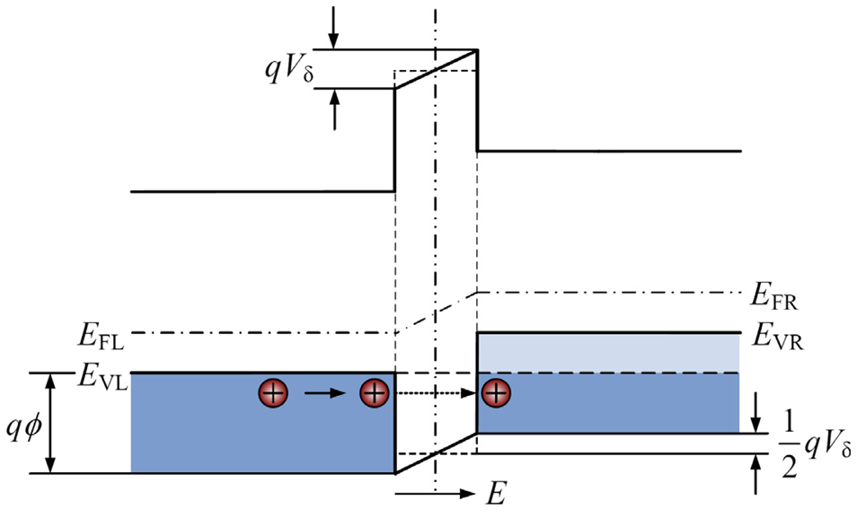
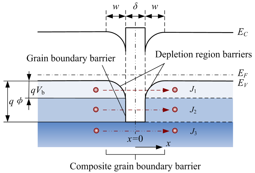
Theoretically, carriers pass through GBs by two transport mechanisms of thermionic emission and tunneling. For simplification, the carrier transport is considered to be one-dimensional. So, according to the kinetic energy
Ex of carriers, there are three current components in the conduction current of carriers traversing GBs (
Figure 7), where
w, δ, qϕ and
qVb are the DRB width, the GB width, the GB barrier height and the DRB height, respectively. At very low temperatures,
Ex<
qVb, carriers traverse the composite GBs only by tunneling, forming the field emission current
J1; At intermediate temperatures,
qVb<
Ex<
qϕ, carriers cross the DRBs by thermionic emission and penetrate the GB barrier by tunneling, forming the composite current
J2; At very high temperatures,
Ex>
qϕ, carriers traverse the composite GB completely by thermionic emission, forming the thermionic emission current
J3. In the temperature range of polysilicon devices working,
J2 is dominant, and
J1 and
J3 could be neglected [
25].
In our tunneling piezoresistive model, the piezoresistive effect of GBs is due to that the stress-induced deformation gives rise to the split-off of the degenerate heavy and light hole sub-bands, thereby causing the carrier transfer between two bands and the conduction mass shift. Inside each grain, due to the single crystal nature of grain neutral regions, the GF of this regions, GFg, is dependent on the PRC of Si single crystals, πg. The GF of composite GBs, GFb, is dependent on the PRC of DRBs (πd) and the PRC of GB barriers (πδ). Hence, in order to explain the piezoresistive behavior of PSNFs with different deposition temperatures theoretically, it is necessary to deduce the relationship between πg, πd and πδ.
For DRBs, based on the dependence of thermionic emission current on strain, the relational expressions of longitudinal PRC
πdl and transversal PRC
πdt in the [111] orientation have been derived in our previous work [
28] and expressed as:
where
πgl and
πgt are the longitudinal and transversal PRCs of p-type monocrystalline silicon in the [111] orientation, respectively.
3.2. Tunneling current through grain boundary barriers
Before deducing the PRC
πδ, the conduction current of carriers penetrating GB barriers must be determined.
Figure 8 provides the energy band diagram and tunneling mechanism of GB barrier omitting DRBs. It is assumed that the voltage drop over the GB barrier is
Vδ. Using Fermi-Dirac statistics, the number of holes having energy within the range d
Ex incident from left to right on the GB barrier per unit time per unit area is [
29]:
where
md is the effective mass of holes for state density,
ξ =
EF - EV, is the difference of Fermi level and valence band edge,
h is Planck's constant,
k is Boltzmann's constant,
T is the absolute temperature.
The GB width
δ is very small (around 1nm), and the number of the holes with high energies around
qϕ is few. Hence, when calculating the current density, the oblique distribution of energy band at the top of GB barrier in
Figure 8 can be substituted by the horizontal line approximately. So, the probability of carriers with the energy
Ex (0 ≤
Ex ≤
qϕ −
qVδ/2) tunneling the GB barrier is given by:
where
mi is the hole effective mass in the tunneling direction. In
Figure 8, the left valence band edge
EVL is taken to be the zero point of energy. By deducing from
Eqs. (6)-
(8), the current density of holes tunneling GB barrier from left to right is:
The current density of holes tunneling GB barrier from right to left is:
By simplifying the logarithmic term in
Eq. (6) into the exponential form,
Eq. (9) can be expressed as:
Considering the fact that the holes gather mostly near the valence band edge, when solving the integration in
Eq. (12), the square root term is expended by the Taylor's series as follows:
Substituting
Eq. (13) into
Eq. (7),
Eq. (12) can be solved out by integrating:
where
Similarly,
Then, the current density of tunneling the GB barrier can be given by:
where
In the case of low voltage bias (
qVδ ≪
kT), the exponential terms in
Eq. (17) can be expanded by using the Taylor's series. After taking the first order approximation, it yields:
Considering the hole concentration formula:
and then
Eq. (19) can be rewritten as:
When two sub-bands split off under an axial stress, the total tunneling current (
Jδ) consists of tunneling currents of heavy holes (
Jδ1) and light holes (
Jδ2) and can be expressed as:
where
Jδj is the tunneling current component of degenerate sub-band,
pj is the corresponding hole concentration, the subscript
j=1, 2, represents the heavy and light hole sub-bands, respectively.
3.3. Piezoresistance coefficient of grain boundary barriers
When the heavy and light hole sub-bands split off under stress, the band shift
ε′ is defined as the shift of two split-off sub-bands (
EV1 and
EV2) relative to the initial degenerate band (
EV). For the sake of simplification, the applied axial stress is assumed to be along the <111> orientation. According to the result of the cyclotron resonance experiment by Hensel and Feher [
30], the effective mass of holes under an axial stress is obtained in
Table 1, where
mlj and
mtj are the longitudinal and transversal effective mass of holes at the sub-band
EVj, respectively.
The split-off heavy and light hole sub-bands are
EV+
ε′ and
EV-
ε′, respectively. By differentiating
Eq. (20) and substituting d
EV by
ε′, the concentration changes of two sorts of holes are, respectively:
When the uniaxial stress is
σ̄, the band shift
ε′ is [
30]:
where
Du is deformation potential constant,
C44 is the corresponding elastic stiffness constant. Due to the different effective mass of heavy and light holes, the change in the corresponding hole concentra-tions can lead the tunneling current
Jδ to vary, which is the principle of tunneling piezoresistive effect. The relative change of the equivalent tunneling resistivity is:
From
Eqs. (21)-
(23), it results in:
where (
c1)
j and (
c2)
j can be determined by
Eqs. (15) and
(18), respectively. According to the experiment data provided by Mandurah [
25], the GB width
δ is set to be 1nm and the GB barrier height
qϕ is about 0.6eV. Thus, for heavy holes,
j=1, (
c1)
1 and (
c2)
1 are calculated to be -0.84 and -3.72, respectively; for light holes,
j=2, (
c1)
2 and (
c2)
2 are calculated to be -0.94 and -1.46, respectively. In general,
qVδ ≪
qϕ, it can be obtained from
Eq. (8) that
a ≈
qϕ. From
Eq. (29) and
Table 1, it yields:
Finally, using
Eqs. (26),
(28)-
(31), the longitudinal PRC of GB barriers along the <111> orientation is expressed as:
Similarly, the transversal PRC along <111> orientation is:
From our previous research results, the longitudinal and transversal PRCs of p-type monocrystalline silicon (grain neutral regions) under a uniaxial stress
σ̄ applied along the <111> orientation can be expressed as follows, respectively [
28]:
Comparing
Eqs. (32) and
(33) with
(34) and
(35) accordingly, it yields:
From
Eqs. (36) and
(37), it can be seen that the PRCs
πδ and
πg present a proportional relationship and the PRC
πδ is larger than
πg.
3.4. Piezoresistance coefficient of composite grain boundaries
From the above theoretical analysis, it can be seen that both the PRCs of DRBs and GB barriers are proportional to the PRC of grain neutral regions. Noticeably, according to
Eqs. (4),
(5),
(36) and
(37), the PRC of DRBs
πd is lower than
πg, while the PRC of GB barriers
πδ is higher than
πg. Therefore, the relationship between the PRC of composite GBs
πb and the PRC of grain neutral regions
πg is dependent on the weights of the equivalent resistivity
ρd (for DRBs) and
ρδ (for GB barriers) in the equivalent resistivity
ρb of composite GBs. In this case,
πb can be expressed as:
where
If the potential drops across DRBs on the left and right hand sides of the GB are denoted by VL and VR, respectively; then the potential drops on DRBs and GB barrier are VL+VR and Vδ, respectively. So,
Eq. (38) can be expressed as follows:
where
V0 is the potential drop over the composite GB. Thus, it can be seen that determining the proportional relationship between
VL+
VR and
Vδ is the key to solve out
πb.
Because the polysilicon usually work under low current and low voltage bias, the condition of
VL+
VR<4
Vb can be always satisfied. Then, the relationship of
VL, VR, Vb and
Vδ can be obtained [
25]:
According to the approximation of DRBs, it yields
where
NA is the boron doping concentration,
Nt is the trap density at GBs,
εs and
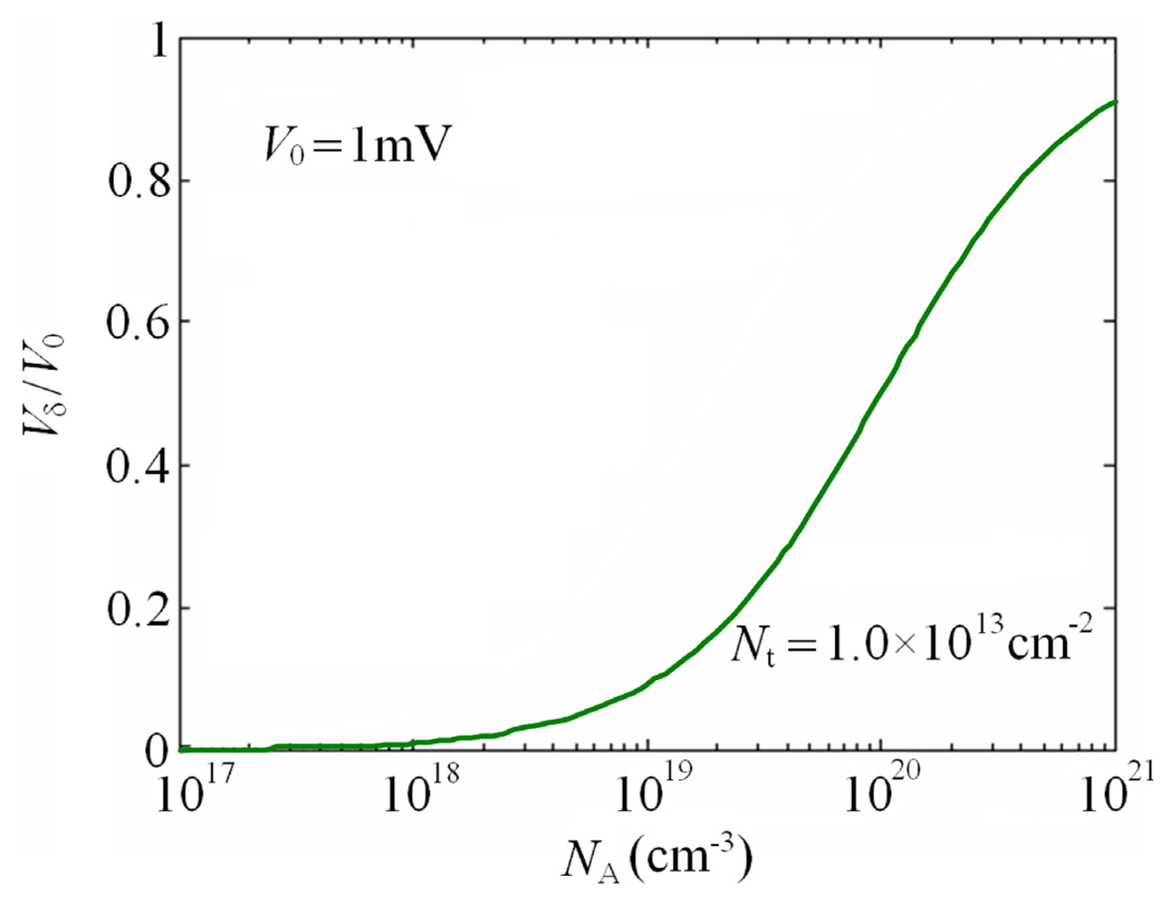
ε0 are the relative and vacuum dielectric constants of Si, respectively. In this paper,
Nt is taken to be 1.0×10
13 cm
-2. By calculating, the distribution of
Vδ normalized to
V0 as a function of
NA is provided in
Figure 9.
By substituting
Eqs. (4),
(5),
(36) and
(37) into
Eq. (39), the relational expression of longitudinal PRCs of composite GBs (
πbl) and grain neutral regions (
πgl) is obtained as:
For p-type monocrystalline silicon, π
11+2π
12 ≪2π
44, it yields [
1]:
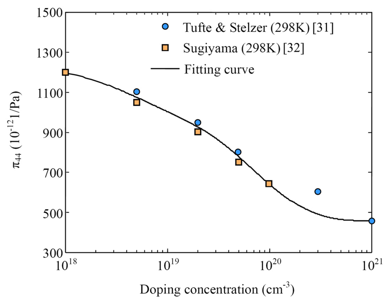
According to the experimental results from Tufte [
31] and Sugiyama [
32], the fitting curve of shear PRC
π44 on
NA is presented in
Figure 10. Consequently, using
Eqs. (46),
(47) and the curves in
Figure 9 and
10, the dependences of the longitudinal PRCs
πbl and
πgl on
NA is obtained, as shown in
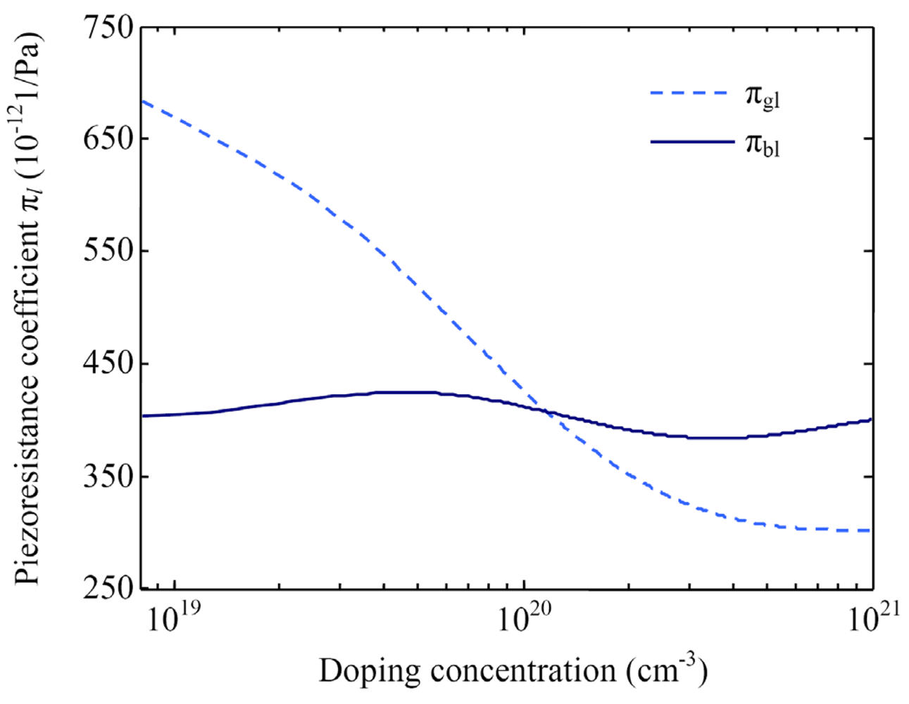
Figure 11. It can be seen that the relationship between the PRC
πbl and
NA is complicated and the variation range of
πbl is smaller than that of
πgl. However, the PRC of composite GBs is larger than that of grain neutral regions at high doping concentrations, which is opposite to the existing models. This conclusion could be used to explain the dependence of GFs on deposition temperature.
3.5. Resistivity and gauge factor versus deposition temperature
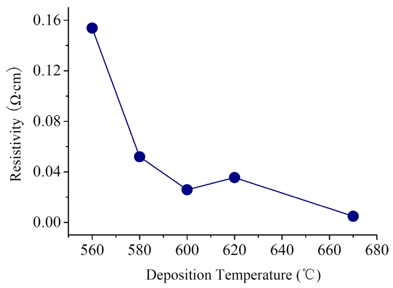
Figure 12 provides the resistivity versus the deposition temperature. It can be seen that the resistivity changes from 1.54×10
-1 to 4.9×10
-3 Ω·cm with elevating deposition temperature. Considering the experiment results that the grain size increases with raising deposition temperature, it indicates that the weight of the resistivity of composite GBs
ρb in the film resistivity
ρ is reduced by increasing deposition temperature. Because
ρb is dependent on the resistivity of GB barriers
ρδ and the resistivity of DRBs
ρd (i.e.,
ρb =
ρδ +
ρd), the elevation of deposition temperature might reduce either of
ρδ and
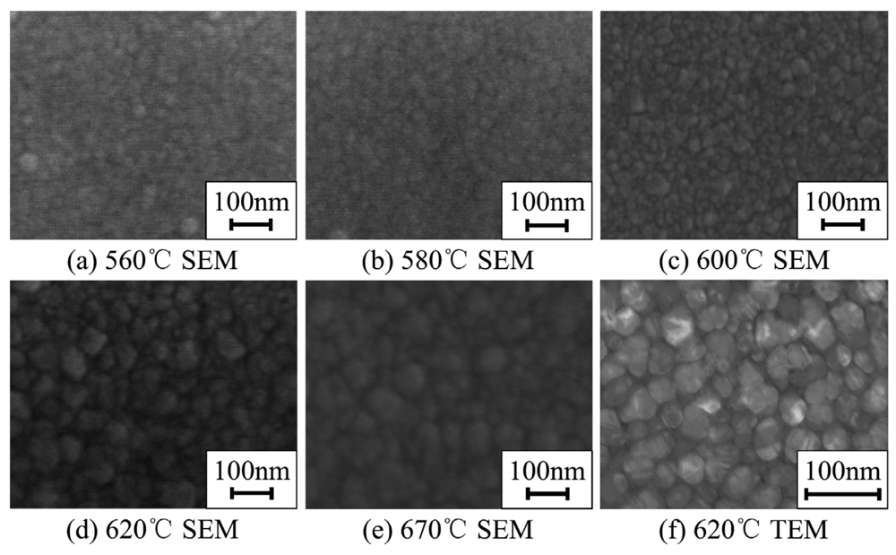
ρd. According to the SEM and XRD results, there are more amorphous contents in RC PSNFs than in DC PSNFs. The existence of amorphous phases at GBs could increase the resistivity
ρδ. On the other hand, the high doping concentration narrows the DRB width to a few angstroms, so that the contribution of
ρd to
ρb could be neglected. Therefore, at high doping concentration, the resistivity
ρb is mainly dependent on the resistivity
ρδ, and the reduction of amorphous contents at GBs caused by elevating deposition temperature is responsible for the falloff of the film resistivity
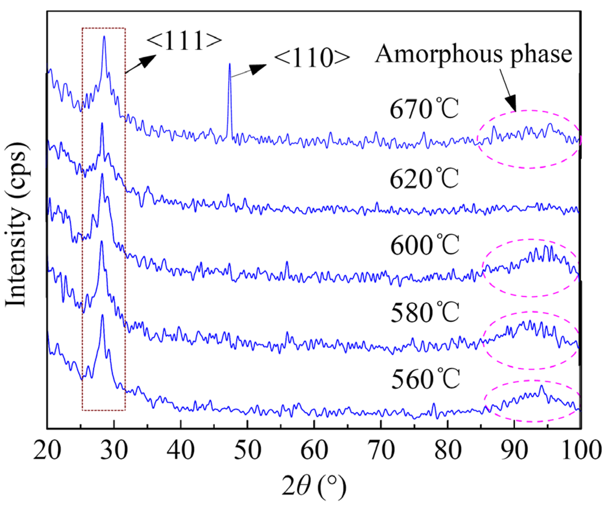
ρ. However, the resistivity of 620°C samples is slightly higher than that of 600°C ones. It is likely due to the recrystallization of 600°C samples after the pre-annealing at 950°C, which is discussed in details in the next section.
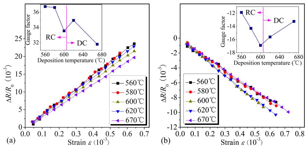
The dependences of the resistance change Δ
R/
R0 in longitudinal and transversal piezoresistors on the strain
ε with different deposition temperatures are shown in
Figures 13(a) and (b), respectively. Obviously, the longitudinal and transversal piezoresistances vary linearly with the strain. From the insets of
Figure 13(a) and (b), it can be seen that RC PSNFs and DC PSNFs exhibit different piezoresistive properties. And the critical deposition temperature differentiating RC PSNFs and DC PSNFs is around 605°C. The samples deposited below this critical temperature present amorphous appearance mixed with polycrystals, while the samples above this value present better polysilicon appearance. This critical value is consistent with the result by French
et al. [
15].
For the longitudinal piezoresistive sensitivity, it can be seen in
Figure 13(a) that the GFs of RC or DC PSNFs decrease with elevating deposition temperature. As discussed above, the amorphous contents at GBs are reduced by raising deposition temperature. For RC PSNFs, when the deposition temperature is lowered, the crystallinity of samples is aggravated and there are more amorphous phases existing at GBs. The increase of amorphous phases raises the resistivity
ρδ. Moreover, the deficient crystallinity increases the width of GB barriers
δ and further increases the weight of
ρb in the film resistivity
ρ. According to the existing piezoresistive model, the PRCs of DRBs (
πd) and GB barriers (
πδ) are lower than that of grain neutral regions
πg. Thus, it implies that the piezoresistive sensitivity of PSNFs with more amorphous contents and smaller grain size should be much lower. However, it is obvious that the deduction is inconsistent with the experiment results. Based on the tunneling piezoresistive theory presented here, the longitudinal PRC of composite GBs
πbl is much larger than that of grain neutral regions
πgl at high doping concentration. As a result of lowering deposition temperature, both the resistivity
ρb and the weight of
ρb in the film resistivity
ρ increase. It enhances the contribution of the PRC
πbl on the piezoresistive sensitivity, thereby increasing longitudinal GFs. For DC PSNFs, the XRD analysis indicates that there are more amorphous phases in the 670°C samples than in the 620°C ones, which is likely due to the <110> preferred growth aggravating disordered states of GBs. It makes the resistivity
ρδ of 670°C samples higher than 620°C samples. However, the SEM results show that the grain size of 670°C samples is ∼70nm and much larger than that of 620°C ones. This reduces severely the weight of the resistivity
ρb in the film resistivity
ρ and weakens the contribution of the PRC
πbl on the piezoresistive sensitivity. Therefore, the longitudinal GF of 670°C samples with larger grains is much lower than that of 620°C ones.
For the transversal piezoresistive sensitivity, the inset of
Figure 13(b) shows that the magnitude of the transversal GF in DC PSNFs increases with lowering deposition temperature, similar to the longitudinal GF dependence; while the magnitude of the transversal GF in RC PSNFs falls off drastically with lowering deposition temperature. Comparing the insets of
Figure 13(a) and (b), it can be seen that the longitudinal GF of DC PSNFs is about twice larger than the transversal one. However, the longitudinal and transversal GFs of RC PSNFs do not satisfy the above proportional relation. On the contrary, the transversal GF of RC PSNFs decreases from 1/2 to 1/3 of the longitudinal one with lowering deposition temperature, which might be due to the degradation of transversal piezoresistive effect in amorphous silicon.
It is noteworthy that the stress-induced modulation of surface depletion region width in silicon nanowires [
3] is not fit for the explanation of enhanced piezoresistive effect in PSNFs. For silicon nanowires, the surface depletion regions are parallel to the direction of carrier transport, and the change in surface potential barrier caused by stress only influences the conducting channel width of carriers along silicon nanowires. However, for PSNFs, the depletion regions are perpendicular to the direction of carrier transport and the carriers have to traverse them by thermionic emission or tunneling. Moreover, the depletion region width is reduced greatly at high doping concentration and can be neglected. So the tunneling effect of carriers becomes dominant.
Although the inset of
Figure 13(a) shows that the longitudinal GFs of 560°C and 580°C samples are slightly higher than those of DC PSNFs, it could not be proven that their sensing performance is better. The reliability and stability have to be also taken into consideration. Therefore, the PRL and RTD of PSNFs were investigated in this paper.
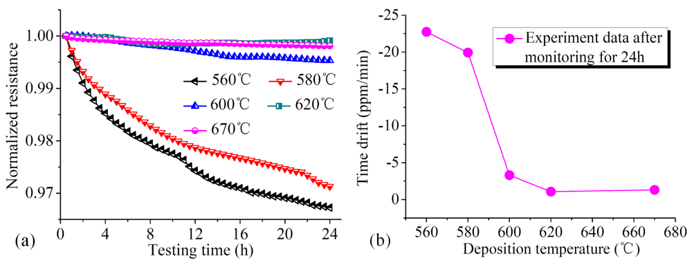
4. Piezoresistive linearity
The PRL of PSNFs is one of significant parameters estimating the static characteristics of piezoresistive sensors. In this section, the IV model is presented to describe the disordered states at GBs of PSNFs. Based on this model, the influence of high temperature annealing on amorphous phases at GBs is analyzed. Finally, the relationship between the PRL and deposition temperature is discussed and explained using this model.
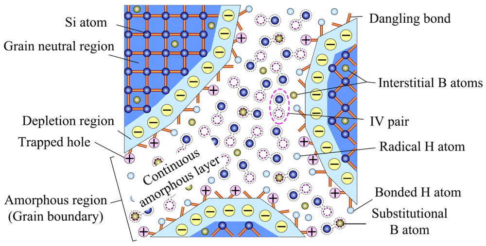
4.1. Interstitial-vacancy model of grain boundaries
Polysilicon is a monatomic silicon material with complex structure. The GBs have a significant impact on the material nature. Particularly, for PSNFs, both the film thickness and the grain size are nanometer sized, so the influence of GBs is enhanced greatly. Furthermore, there are higher amorphous contents existing at GBs of PSNFs, due to insufficient crystallization and fine grains. Thus, the nature of GBs is considered to be amorphous in this paper. In order to describe the amorphous phases at GBs, it is necessary to establish a theoretical model.
According to the work by Marques
et al. [
33], the disordered zones in amorphous silicon can be characterized as the accumulation of interstitial silicon atoms and vacancies. For simplification, these disordered zones are considered as comprised of basic point defects. The point defect structure consists of an interstitial atom and a vacancy and is called interstitial-vacancy pair (IV pair). Similarly, GBs of PSNFs can be modeled by the accumulation of IV pairs.
In the IV model, the amorphous regions at GBs can be classified into continuous amorphous layers (continuous a-layers) and amorphous pockets (a-pockets). And continuous a-layers and a-pockets exhibit similar features. In amorphous regions, the state of each IV pair is dependent on the number of neighboring IV pairs (defined as the IV pair coordination number). Under external energy excitation (e.g., heating, plastic deformation, ion bombardment), an IV pair can overcome the energy barrier of recombination and recombine at a certain probability, similar to the recrystallization of amorphous materials. And the recombination rate increases when the number of neighboring IV pairs decreases. According to the molecular dynamics (MD) calculations by Marques
et al. [
33], the activation energy of the recombination of an isolated IV pair is 0.43eV, while the IV pairs within amorphous regions (surrounded completely by neighboring IV pairs, hence with the full IV pair coordination number) have the activation energy of 5eV. Moreover, it should be noted that the IV pairs located at a planar amorphous/crystal (a/c) interface (with about half of the full coordination number) have the activation energy of 2.7eV [
34]. It indicates that the activation energy of IV pair recombination and the number of neighboring IV pairs satisfy the linear interpolation relationship approximately. Thus, the distribution of neighboring IV pairs determines the recombination rate and activation energy of an IV pair.
For continuous a-layers, all the IV pairs at an a/c interface have the same number of neighboring IV pairs, and therefore the same recombination rate. Because the IV pairs at an a/c interface have fewer neighboring IV pairs than in inner zones, the recombination of IV pairs takes place at the a/c interface firstly. It starts a cascade mechanism in which IV pairs could recombine layer by layer. A-pockets show a similar recombination behavior [
35]. However, due to their irregular and convex shapes, the IV pairs at the surface of a-pockets have different IV coordination numbers (fewer than those of continuous a-layers), so that the recombination active energies are different. The experiments indicate that the recombination of IV pairs in a-pockets is much faster than that of continuous a-layers [
36].
4.2. Influence of high temperature annealing on grain boundaries
The original RC PSNFs exhibit amorphous appearance mixed with polysilicon. Here, it is considered that the amorphous contents include continuous a-layers and a-pockets. Therefore, the pre-annealing was performed at 950°C for 30 min to induce the recrystallization of amorphous contents. However, even after the post-implantation annealing at 1080°C, the SEM and XRD results show that there are still many amorphous contents existing at GBs. It indicates that the further recrystallization of amorphous contents was prevented in the temperature range of 950∼1080°C. This is likely related to the concentration of IV pairs at GBs.
The MD simulation results by Marques
et al. [
33] show that when the temperature is around 1200 K, IV pairs with a concentration of 25% in amorphous regions produce polycrystalline material; when the temperature is higher than 1200 K and even 1600 K, IV pairs with a concentration of 25% generate amorphous matrix again. For IV pairs with a concentration of 10-20%, the recrystallization takes place in the temperature range between 1000 and 2000 K. For RC PSNFs, the experiments indicate that the pre-annealing of 950°C (≈1220 K) gives rise to the recrystallization of amorphous contents at GBs and the increase of polysilicon contents, but the post-implantation annealing of 1080°C (≈1350 K) increases amorphous contents to a certain extent. Consequently, the concentration of IV pairs at GBs of RC PSNFs is estimated to be about 25%. For PSCFs, the experimental results show that the annealing of 1080°C can increase the grain size and improve the film crystallinity [
15]. It can be considered that GBs of PSCFs contain IV pairs with a concentration of 10-20%. This verifies that the crystallinity of RC PSNFs is worse than that of PSCFs and there are more amorphous phases at GBs of RC PSNFs.
In this paper, a-pockets with fewer surface IV coordination numbers are considered to be eliminated during the pre-annealing, due to their faster recrystallization rate. Therefore, GBs of PSNFs can be modeled as continuous a-layers, as shown in
Figure 14. Boron dopants are ion-implanted into PSNFs, forming the interstitial atoms and substitutional atoms. The occupation of substitutional boron atoms to the vacancies also suppresses the recrystallization of IV pairs.
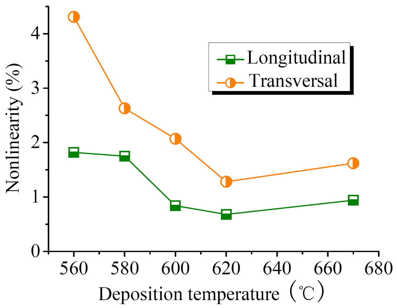
4.3. Piezoresistive nonlinearity versus deposition temperature
The dependences of PRNL of longitudinal and transversal PSNF piezoresistors on deposition temperature are given in
Figure 15. Obviously, the PRL of longitudinal piezoresistors is superior to the transversal ones. It should be noted that the PRNL of RC PSNFs and 670°C samples is higher than 620°C samples, indicating that amorphous phases at GBs are the origin of PRNL. In the case of room temperature and small stresses, only the first-order PRCs are taken into account, and the nonlinear piezoresistance effects (high-order PRCs) in silicon [
37] could be neglected. Therefore, the conditions of GBs make a significant impact on the PRL.
In the IV model, GBs are considered to be the accumulation of IV pairs and behave as continuous a-layers. According to the simulation results by Marques
et al. [
33], the IV pair is not stable and the lifetime of an isolated IV pair is only 3μs at room temperature. Even though an isolated IV pair is unstable (the energy barrier of recombination is only 0.43eV), the accumulation of IV pairs could increase the active energy to 5eV (in amorphous matrix) and improve the stability of IV pairs. However, there are still unstable IV pairs existing at GBs, they could recombine under external energy excitation. Due to the existence of GBs as a metastable non-crystal structure, polysilicon is not an absolute rigid material. The slight plastic deformation could occur, when a stress is applied to the material. Similar to the crystallization induced by deformations in non-crystal metals [
38], the deformation could increase the energies of inner atoms at GBs and cause some unstable IV pairs (with low energy barrier of recrystallization) to recombine. The recombination of IV pairs caused by material deformation leads the number of scattering centers to change, thereby resulting in the minute variation of film resistivity. This might be one of the prime reasons for PRNL. It should be noted that the change in resistivity caused by the recrystallization of IV pairs is very little and can not influence the change trend of resistance for piezoresistive effect.
Considering the type of applied stresses, the longitudinal piezoresistive effect is caused by tension stress, while the transversal piezoresistive effect is caused by compression stress. The experiment results based on metal materials show that the compression stress has a more remarkable role in stress-induced crystallization than tension stress. Similarly, it is believed that the recombination of IV pairs under compression stress is more prominent. Consequently, the PRNL of transversal piezoresistors is higher than that of longitudinal ones, which is in good agreement with the experimental results in
Figure 15. On the other hand, based on the explanations presented in our previous research work [
39], the higher amorphous contents increase trap density at GBs, resulting in that the probability of traps capturing heavy and light holes could change. This might be the secondary reason for PRNL.
Finally, the experimental results indicate that the 620°C PSNFs with the lowest amorphous contents have the best PRL. Although the high temperature annealing could improve the crystallinity of RC PSNFs, a large number of residual amorphous contents at GBs still produce the higher PRNL. It testifies that the disordered states of GBs determine the PRL of PSNFs.
6. Conclusions
In this paper, the piezoresistive sensitivity, PRL and RTD of highly boron doped LPCVD PSNFs were studied, and the influences of deposition temperature and high temperature annealing on the above-mentioned properties were analyzed. As for the tunneling piezoresistive effect, the tunneling piezoresistive model was established. The carrier transport mechanisms across GBs are considered to be thermionic emission and tunneling, and the tunneling current becomes dominant at high doping concentration. By theoretical calculation, a conclusion was drawn that the PRC of composite GBs is higher than that of grain neutral regions at high doping concentration. The dependences of longitudinal and transversal GFs on deposition temperature were obtained. The results indicate that the piezoresistive properties of the RC PSNFs are different from the DC ones. According to SEM and XRD results, it is considered that amorphous contents at GBs and grain size are important factors influencing the piezoresistive properties of PSNFs. The magnitude of GF is dependent on the equivalent resistivity of GB barriers and the weight of the resistivity of composite GBs in the film resistivity.
In the investigations on PRL and RTD of PSNF piezoresistors, the IV model was established to describe the nature of GBs. In our model, GBs are regarded as the accumulation of IV pairs. The PRNL is due to the reduction in the number of scattering centers caused by the stress-induced recrystallization of metastable IV pairs at GBs. For RTD of PSNFs, it is considered as due to the recombination of minority IV pairs under low field current excitation. And the motion of residual hydrogen atoms at GBs is also taken into account. Consequently, the conclusions were drawn that the deposition temperature is one of the significant parameters determining the nature of PSNFs. Optimizing the structure of grains and GBs by controlling deposition temperature could improve the piezoresistive performance of PSNFs. Even though the high temperature annealing could induce the recrystallization of amorphous contents at GBs, the transfer from amorphous phases to polycrystalline phases is dependent on the concentration of IV pairs at GBs and annealing temperature. The high temperature annealing on the PSNFs with high concentration (∼25%) of IV pairs is not very effective in improving the reliability and stability of the material. Finally, it is obtained that the optimal deposition temperature is about 620°C.


