A CMOS-Compatible, Low-Noise ISFET Based on High Efficiency Ion-Modulated Lateral-Bipolar Conduction

Abstract
:
1. Introduction
2. Experimental Section
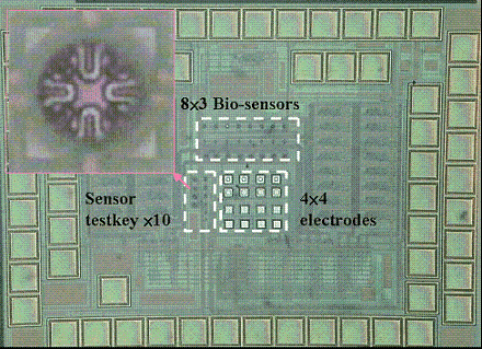
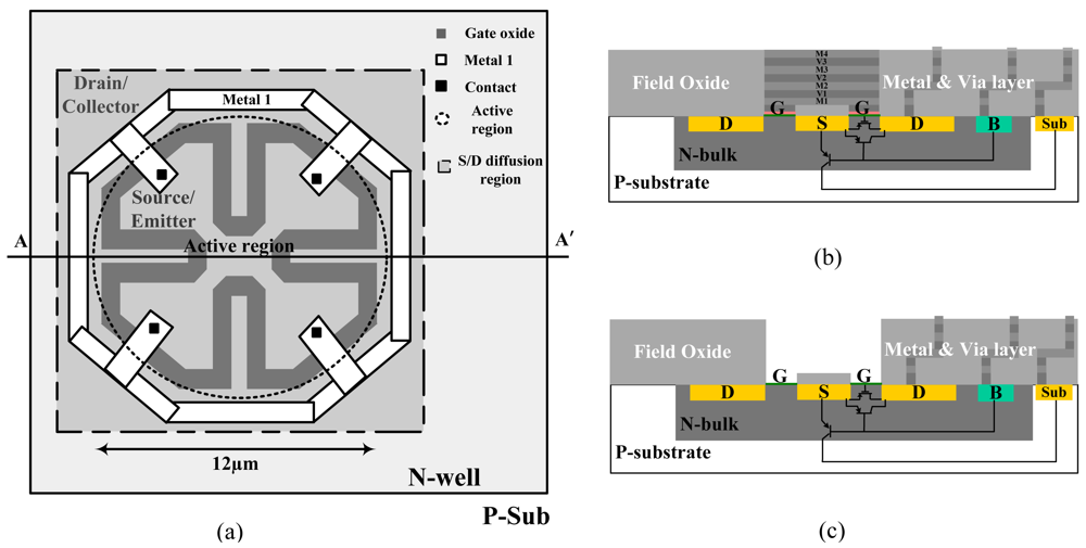
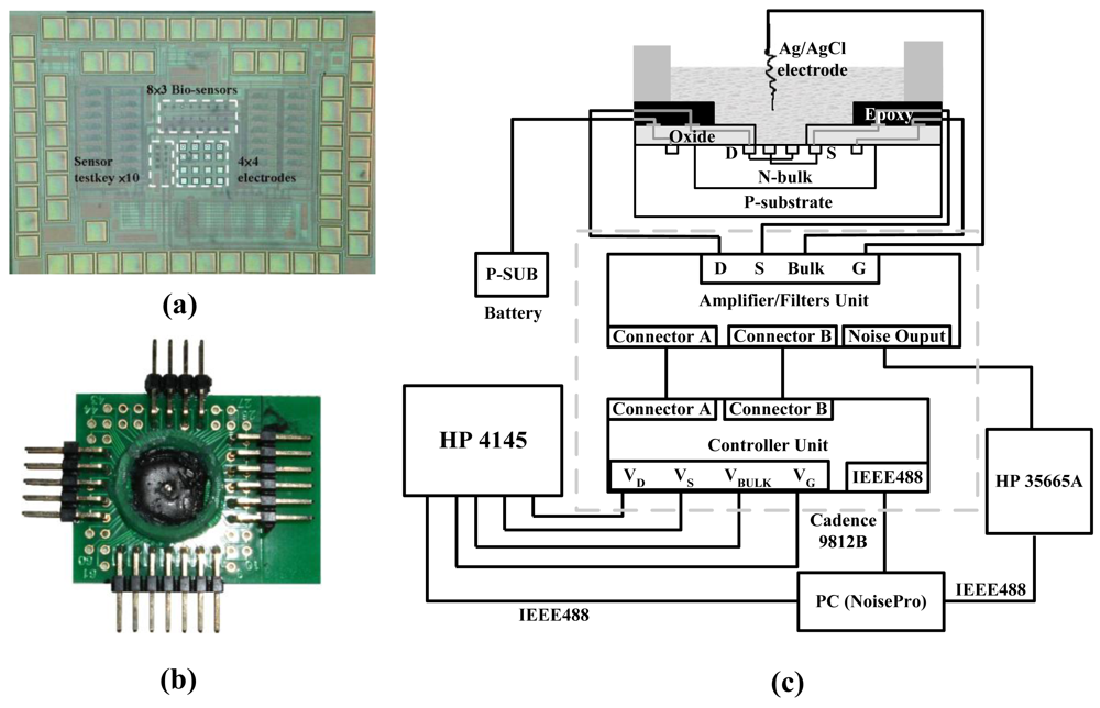
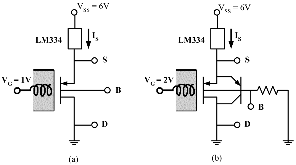
2.1. The layout and the structure of the ISFET
2.2. The post-CMOS process
2.3. Noise Measurement
2.4. pH Sensing
3. Results and Discussion
3.1. Device fabrication
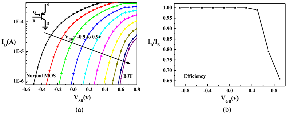
3.2. Operation modes and efficiency
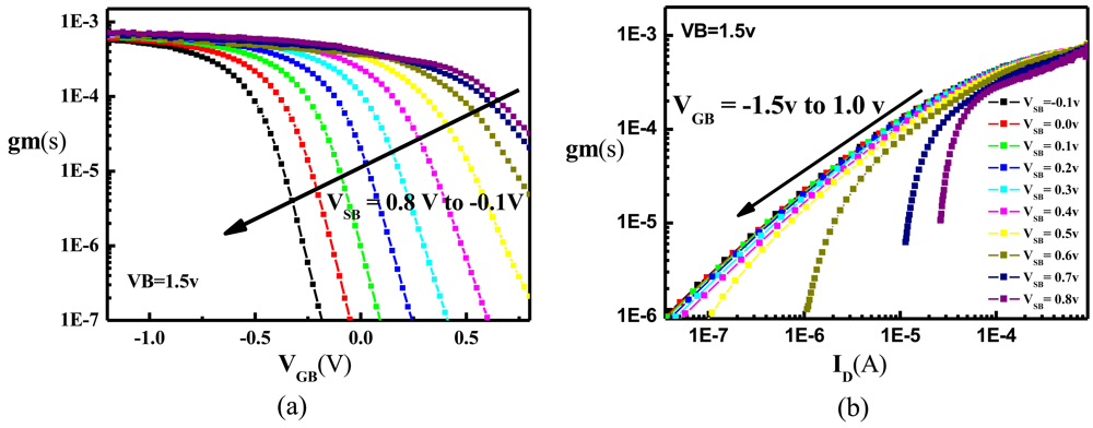
3.3. Transconductance
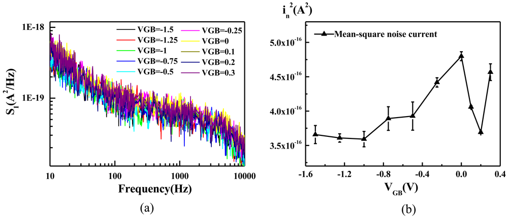
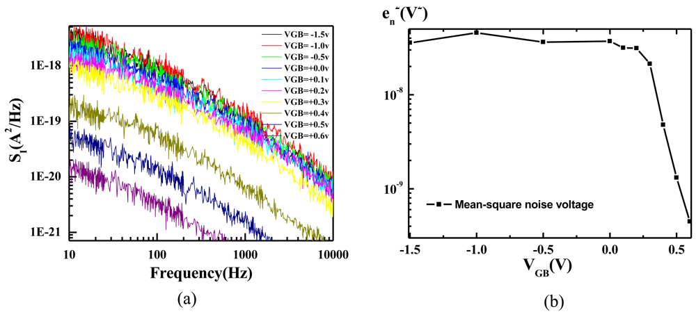
3.4. Noise performance with constant ID
3.5. Noise performance with constant gm
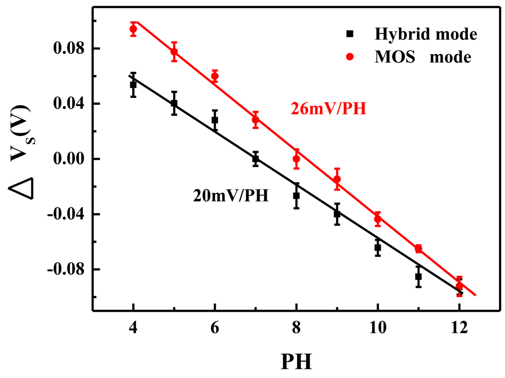
3.6. pH sensing
4. Conclusions
Acknowledgments
References and Notes
- Bergveld, P. Thirty years of ISFETOLOGY What happened in the past 30 years and what may happen in the next 30 years. Sens. Actuat. B: Chem. 2003, 88, 1–20. [Google Scholar]
- Kim, D.S.; Jeong, Y.T.; Park, H.J.; Shin, J.K.; Choi, P.; Lee, J.H.; Lim, G. An FET-type charge sensor for highly sensitive detection of DNA sequence. Biosens. Bioelectron. 2004, 20, 69–74. [Google Scholar]
- Dzyadevych, S.V.; Soldatkin, A.P.; El'skaya, A.V.; Martelet, C. Enzyme biosensors based on ion-selective field-effect transistors. Anal. Chim. Acta 2006, 568, 248–258. [Google Scholar]
- Fromherz, P.; Carsten, O.; Weis, R. Neuron transistor: Electrical transfer function measured by the patch-clamp technique. Phys. Rev. Lett. 1993, 71, 4079–4082. [Google Scholar]
- Fromherz, P.; Offenhausser, A. A neuron-silicon junction: A Retzius cell of the leech on an insulated-gate field-effect transistor. Science 1990, 252, 1290–1293. [Google Scholar]
- Hutzler, M.; Fromherz, P. Silicon chip with capacitors and transistors for interfacing organotypic brain slice of rat hippocampus. Eur. J. Neurosci. 2004, 19, 2231–2238. [Google Scholar]
- Milgrew, M.J.; Riehle, M.O.; Cumming, D.R.S. A large transistor-based sensor array chip for direct extracellular imaging. Sens. Actuat. B 2005, 111, 347–353. [Google Scholar]
- Hizawa, T.; Sawada, K.; Takao, H.; Ishida, M. Fabrication of a two-dimensional ph image sensor using a charge transfer technique. Sens. Actuat. B 2006, 117, 509–515. [Google Scholar]
- Eversmann, B.; Jenkner, M.; Hofmann, F.; Paulus, C.; Brederlow, R.; Holzap, B.; Fromherz, P.; Merz, M.; Steinhauser, M.M.; Eckstein, G; Schmitt-Landsiedel, D.; Thewes, R. A 128 × 128 CMOS biosensor array for extracellular recording of neural activity. IEEE J. Solid-State Circ. 2003, 38, 2306–2317. [Google Scholar]
- Parak, W.J.; George, M.; Gaub, H.E.; Bohm, S.; Lorke, A. The field-effect-addressable potentiometric sensor/stimulator (FAPS)Xa new concept for a surface potential sensor and stimulator with spatial resolution. Sens. Actuat. B: Chem. 1999, 58, 497–504. [Google Scholar]
- Hierlemann, A.; Baltes, H. CMOS-based chemical microsensors. Analyst 2003, 128, 15–28. [Google Scholar]
- Joo, S.; Brown, R.B. Chemical sensors with integrated electronics. Chem. Rev. 2008, 108, 638–651. [Google Scholar]
- Bausells, J.; Carrabina, J.; Errachid, A.; Merlos, A. Ion-sensitive field-effect transistors fabricated in a commercial cmos technology. Sens. Actuat. B 1999, 57, 56–62. [Google Scholar]
- Hammond, P.A.; Ali, D.; Cumming, D.R.S. Design of a single-chip ph sensor using a conventional 0.6μm CMOS process. IEEE Sens. J. 2004, 4, 706–712. [Google Scholar]
- Hammond, P.A.; Ali, D.; Cumming, D.R.S. A system-on-chip digital ph meter for use in a wireless diagnostic capsule. IEEE Trans. Biomed. Eng. 2005, 52, 687–694. [Google Scholar]
- Bergveld, P. BME-19. Development, operation, and application of the ion-sensitive field-effect transistor as tool for electrophysiology. IEEE Trans. Biom. Eng. 1972, 342–351. [Google Scholar]
- Eversmann, B.; Jenkner, M.; Hofmann, F.; Paulus, C.; Brederlow, R.; Holzapfl, B.; Fromherz, P.; Merz, M.; Brenner, M.; Schreiter, M.; Gabl, R.; Plehnert, K.; Steinhauser, M.; Eckstein, G.; Schmitt-Landsiedel, D.; Thewes, R. A 128 × 128 CMOS biosensor array for extracellular recordingof neural activity. IEEE J. Solid-State Circ. 2003, 38, 2306–2317. [Google Scholar]
- Lambacher, A.; Jenkner, M.; Merz, M.; Eversmann, B.; Kaul, R.A.; Hofmann, F.; Thewes, R.; Fromherz, P. Electrical imaging of neuronal activity by multi-transistor-array (MTA) recording at 7.8μm resolution. Appl. Phys. A-Mater. Sci. Process. 2004, 79, 1607–1611. [Google Scholar]
- Chin, Y.L.; Chou, J.C.; Sun, T.P.; Chung, W.Y.; Hsiung, S.K. A novel ph sensitive isfet with on-chip temperature sensing using CMOS standard process. Sens. Actuat. B 2001, 76, 582–593. [Google Scholar]
- Chin, Y.L.; Chou, J.C.; Sun, T.P.; Liao, H.K.; Chung, W.Y.; Hsiung, S.K. A novel SnO2/Al discrete gate ISFET ph sensor with CMOS standard process. Sens. Actuat. B 2001, 75, 36–42. [Google Scholar]
- Lauwers, E.; Suls, J.; Gumbrecht, W.; Maes, D.; Gielen, G.; Sansen, W. A CMOS multiparameter biochemical microsensor with temperature control and signal interfacing. IEEE J. Solid-state Circ. 2001, 36, 2030–2038. [Google Scholar]
- Witvrouw, A.; Steenkiste, F.V.; Maes, D.; Haspeslagh, L.; Gerwen, P.V.; Moor, P.D.; Sedky, S.; Hoof, C.V.; Vries, A.C.; Verbist, A.; Caussemaeker, A.D.; Parmentier, B.; Baert, K. Why CMOS-integrated transducers? A review. Microsyst. Technol. 2000, 6, 192–199. [Google Scholar]
- Chang, S.R. Die-level, post-CMOS processes for fabricating open-gate, field-effect biosensor arrays with on-chip circuitry. J. Micromech. Microeng. 2008, 18, 115032. [Google Scholar]
- Harrison, R.R. A versatile integrated circuit for the acquisition of biopotentials. Proceedings of IEEE Custom Integrated Circuits Conference, San Jose, CA, USA, September 16–19, 2007; pp. 115–122.
- Deen, M.J.; Levinshtein, M.E.; Rumyantsev, S.L.; Orchard-Webb, J. Generation-recombination noise in MOSFETs. Semicond. Sci. Technol. 1999, 14, 298–304. [Google Scholar]
- Phillip, E.A.; Douglas, R.H. CMOS Analog circuit Design, 2nd Ed. ed; Oxford University: New York, NY, USA, 2002; pp. 408–409. [Google Scholar]
- Deen, M.J.; Marinov, O. Effect of forward and reverse substrate biasing on low-frequency noise in silicon PMOSFETs. IEEE Trans. Electron Dev. 2002, 49, 409–413. [Google Scholar]
- Vandamme, L.K.J.; Li, X.; Rigaud, D. 1/f noise in MOS devices, mobility or number fluctuations? IEEE Trans. Electron Dev. 1994, 41, 1936–1945. [Google Scholar]
- Vittoz, E.A. MOS transistors operated in the lateral bipolar mode and their application in CMOS technology. IEEE J. Solid-State Circ. 1983, 18, 273–279. [Google Scholar]
- Holman, W.T.; Connelly, J.A. A compact low noise operational amplifier for a 1.2 μm digital CMOS technology. IEEE J. Solid-State Circ. 1995, 30, 710–714. [Google Scholar]
- MacSweeney, D.; McCarthy, K.G.; Mathewson, A.; Mason, B. A SPICE compatible subcircuit model for lateral bipolar transistors in a CMOS process. IEEE Trans. Electron Dev. 1998, 45, 1978–1984. [Google Scholar]
- Chung, W.Y.; Yang, C.H.; Pijanowska, D.G.; Grabiec, P.B.; Torbicz, W. ISFET performance enhancement by using the improved circuit techniques. Sens. Actuat. B: Chem. 2006, 113, 555–562. [Google Scholar]
- Bousse, L.; Shott, J.; Meindl, J.D. A process for the combined fabrication of ion sensors and CMOS circuits. IEEE Electron Dev. Lett. 1988, 9, 44–46. [Google Scholar]
- Chang, C.H.; Chang, S.R.; Lin, J.S.; Lee, Y.T.; Yeh, S.R.; Chen, H. A CMOS neuroelectronic interface based on two-dimensional transistor arrays with monolithically-integrated circuitry. Biosens. Bioelectron. 2009, 24, 1757–1764. [Google Scholar]


© 2009 by the authors; licensee Molecular Diversity Preservation International, Basel, Switzerland. This article is an open access article distributed under the terms and conditions of the Creative Commons Attribution license (http://creativecommons.org/licenses/by/3.0/).
Share and Cite
Chang, S.-R.; Chen, H. A CMOS-Compatible, Low-Noise ISFET Based on High Efficiency Ion-Modulated Lateral-Bipolar Conduction. Sensors 2009, 9, 8336-8348. https://doi.org/10.3390/s91008336
Chang S-R, Chen H. A CMOS-Compatible, Low-Noise ISFET Based on High Efficiency Ion-Modulated Lateral-Bipolar Conduction. Sensors. 2009; 9(10):8336-8348. https://doi.org/10.3390/s91008336
Chicago/Turabian StyleChang, Sheng-Ren, and Hsin Chen. 2009. "A CMOS-Compatible, Low-Noise ISFET Based on High Efficiency Ion-Modulated Lateral-Bipolar Conduction" Sensors 9, no. 10: 8336-8348. https://doi.org/10.3390/s91008336