Effect of Electrical Contact on the Contact Residual Stress of a Microrelay Switch

1
Department of Vehicle Engineering, National Pingtung University of Science and Technology, Pingtung, Taiwan
2
Department of Biomechatronics Engineering, National Pingtung University of Science and Technology, Pingtung, Taiwan
3
Department of Material Engineering, National Pingtung University of Science and Technology, Pingtung, Taiwan
*
Author to whom correspondence should be addressed.
Sensors 2007, 7(11), 2997-3011; https://doi.org/10.3390/s7112997
Submission received: 12 October 2007
/
Accepted: 14 November 2007
/
Published: 26 November 2007
(This article belongs to the Special Issue Modeling, Testing and Reliability Issues in MEMS Engineering)
Abstract
:This paper investigates the effect of electrical contact on the thermal contact stress of a microrelay switch. A three-dimensional elastic-plastic finite element model with contact elements is used to simulate the contact behavior between the microcantilever beam and the electrode. A model with thermal-electrical coupling and thermal-stress coupling is used in the finite element analysis. The effects of contact gap, plating film thickness and number of switching cycles on the contact residual stress, contact force, plastic deformation, and temperature rise of the microrelay switch are explored. The numerical results indicate that the residual stress increases with increasing contact gap or decreasing plating film thickness. The results also show that the residual stress increases as the number of switching cycles increases. A large residual stress inside the microcantilever beam can decrease the lifecycle of the microrelay.
1. Introduction
Microrelays are widely used in the field of electromechanical control, telecommunications, test equipment, and other MEMS devices. The general requirements for microrelays are low power consumption, good insulation, low contact resistance, and good reliability during its lifecycle. Among all types of actuation of the microrelay, the electrostatical actuation consumes less power. However, its high driving voltage requires additional circuits in practical applications. The magnetically actuated microrelay has the advantages of large actuating force, large displacement, low driving voltage as well as its insensitivity to the operating environment, which make it popular in many applications. Besides these noticeable features, to be of commercial interest, a magnetically actuated microrelay has to be as reliable as a conventional relay. Although a magnetically actuated microrelay has structural similarities with a conventional relay and can be regarded as a miniature of it, the design of a microrelay should not be as simple as reducing all the dimensions with the same proportions compared with a conventional relay. To function well and to have a good reliability, the knowledge of design parameters, such as the contact gap, plating film thickness of the electrode, contact force, and contact resistance is required.
To improve the reliability of the magnetically actuated microrelay, not many researches have been focused on the study of its design parameters as well as performing characteristics. Hosaka et al. [1] have shown that a gold-gold contact with a contact force greater than 100 μN has a contact resistance lower than 100 mΩ. They also depicted that the cycle lifetime of this device could be improved by a large break force which overcame any contact welding that might occur during switching. Schimkat [2] measured the resistance-force characteristics of AuNi5 contacts after certain cleaning procedure. He found that, at the very low forces following the transition region, the contact resistance was observed to deviate from the relationship derived from Holm's model [3]. In theoretical analysis of microrelay's behaviors, the finite element method is often used, but only few researches are presented. Li and Zhang [4] used the finite element method to do the modal analysis of the microcantilever beam and to analyze the static deflection in the coil center of a magnetically actuated microrelay. The results can help to find a set of logical physical parameters of the microrelay. Norberg et al. [5] used a finite element model to analyze the influence of a thin film constituting at least one of the contacting members of an electrical contact. The error introduced by using the traditional Maxwell/Holm contact constriction resistance theory was investigated. Numerical methods were used to present a way to approximate the total resistance for the thin metal film contact. Lee et al. [6] modeled the residual stress distributions within micro-fabricated bimorph cantilevers of varying thickness. A thermal elastic-plastic finite element model was utilized to calculate the residual stress distribution across the cantilever cross-section and to determine the beam tip deflection following heat treatment. The numerical results indicated that a larger beam thickness led to a greater residual stress difference at the interface between the beam and the film. The residual stress established in the poly-silicon cantilever was greater than that induced in the silicondioxide cantilever.
In this work, the effect of electrical contact on the thermal contact stress of a magnetically actuated microrelay switch is investigated. A three-dimensional elastic-plastic finite element model with contact elements is used to simulate the contact behavior between the microcantilever beam and the electrode. The effects of contact gap, plating film thickness and number of switching cycles on the contact residual stress, contact force, plastic deformation, and temperature rise of the microrelay switch are studied. The simulation data show that the residual stress increases with increasing contact gap or decreasing plating film thickness. The results also show that the residual stress increases with increasing switching cycles. A large residual stress inside the microcantilever beam can decrease the lifecycle of the microrelay.
2. Theoretical Analysis
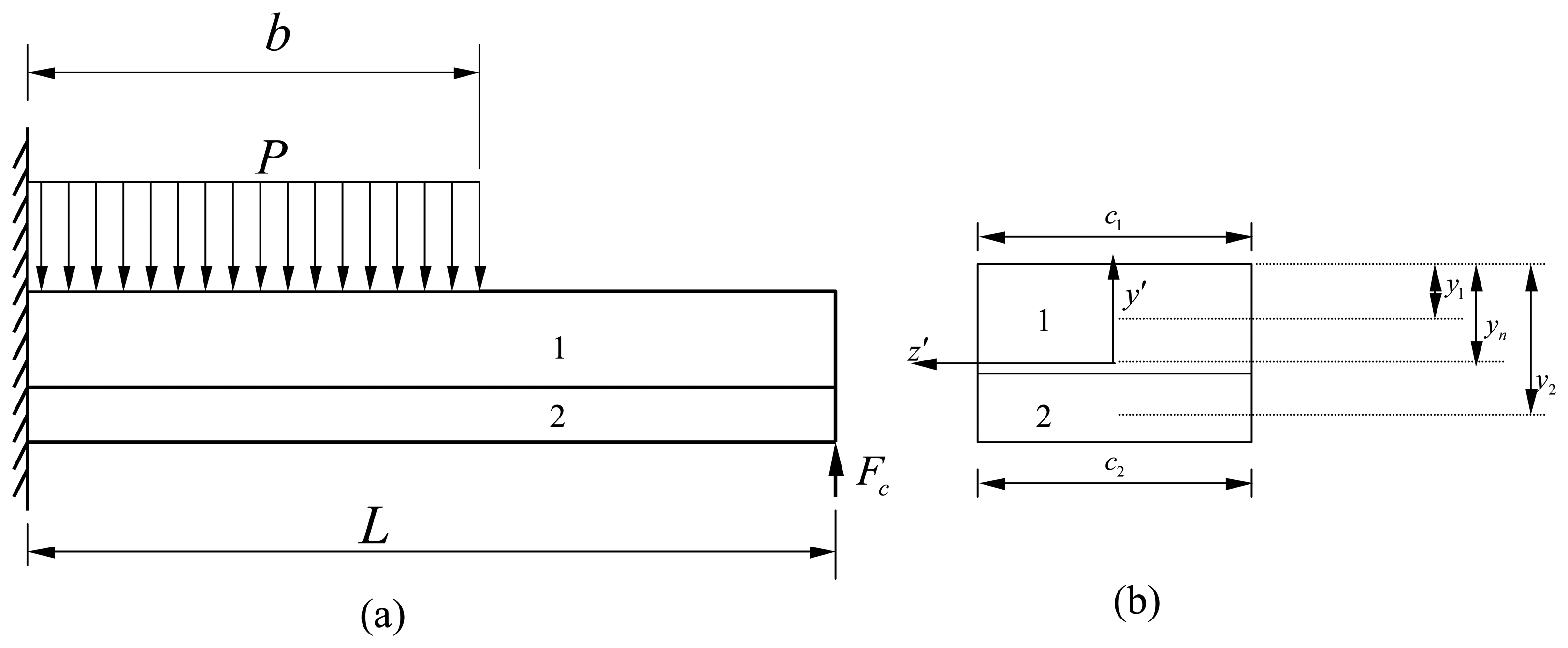
Typically, a microrelay consists of a microcantilever beam, a substrate (electrode) and a fixed support end. Figure 1 presents a schematic illustration of a microrelay and the corresponding geometrical model. In this research, without loss of generality, the length, width and thickness of the microcantilever beam are taken to be 600, 100 and 20 μm, respectively, and the length, width and thickness of the substrate are taken as 80, 100 and 20 μm, respectively. The materials of the microcantilever and the substrate are taken as permalloy and silicon, respectively. In Figure 1, g and γ are denoted as the contact gap and the film thickness, respectively. The other dimensions are shown in Figure 1. Thin Cu films are deposited both on the bottom surface of the microcantilever beam and the top surface of the substrate working as contact electrodes.
Figure 2 presents a schematic illustration of the contact load and the cross section of the microrelay. A uniform pressure P is used to simulate the action of the electromagnetic force. From Figure 1, it can be seen that a contact gap g existed between the microcantilever beam and the electrode when there is no energy supplied. It should be noted that this Cu-filmed electrode also serves to constrain the downward displacement of the microcantilever beam. When the microcantilever beam is actuated, a contact force Fc is created on the contact position, as shown in Figure 2. The thicknesses of the microcantilever beam and the film are denoted as t1 and t2, respectively. The subscripts 1 and 2, hereafter, represent the microcantilever beam and the film, respectively. The mismatch of the thermal expansion coefficients between the film and the beam when the microcantilever beam is subjected to an electromagnetic load induces different thermal deformations on these two components. This establishes residual stresses inside the two components. The neutral axis of the microrelay, as shown in Figure 2, can be obtained by solving the following equation:
where σx1 and σx2 are the bending stresses and can be expressed as:
where κ is the curvature, y' is the distance from the neutral axis as shown in Figure 2, and n is the Young's modulus ratio n=E2 / E1. Equation (1) can be rewritten as
Using the method of transformed section [7], the moment of inertia Ieq of the entire cross-sectional area with respect to the neutral axis can be obtained as
where yn is the distance between the neutral axis and the top surface of the microcantilever beam, y1 and y2 are the distances from the top surface of the microcantilever beam to the centroid of the beam and the film, respectively. From Figure 2, y1 and y2 can be obtained as t1/2 and, t1+ t2/2, respectively. The moment resultant of the bending stresses is equal to the bending moment M acting on the cross section,
Substituting Eqs. (2) and (3) into Eq. (6), the resultant moment M can be expressed as
Since the transformed beam is assumed to be made of only one material, the bending moment can be expressed as
where, from Eqs. (7) and (8), the equivalent Young's modulus Eeq is obtained as
Because the equivalent moment of inertia is Ieq = I1 + nI2 [7], the equivalent Young's modulus Eeq can be obtained as E1. The deflection v and angle of rotation θ of the microcantilever beam as shown in Figure 2 can be expressed as [7]
where b is the area of the region to which the electromagnetic force is applied and L is the length of the microcantilever beam. Thus, the maximum deflection, vmax, at the free end can be obtained by substituting x = b into the following equation:
The deflection, vc, at the free end obtained by applying an electrode contact reaction force Fc can be expressed as
The contact force Fc at the cantilever-electrode contact region can be obtained by adding Eqs. (13) and (14), and equating the result to the contact gap g:
The maximum tensile bending stress σx,max(tensile) can then be derived as
3. Finite Element Model
The effects of film thickness, contact gap and contact force on the contact deformation and residual stress distribution of the microrelay are studied. Three different film thicknesses, i.e. 1, 4 and 6 μm, four different contact gaps, i.e. 1, 5, 10 and 15 μm and four different contact forces, i.e. 1, 10, 15 and 20 mN, are considered in simulations. The origin of the coordinate system xyz is located at the interface of cantilever beam and film as shown in Figure 1 (b).
In this study, a three-dimensional elastic-plastic finite element model is used to simulate the electrical contact between the microcantilever beam and the electrode. The numerical simulations are performed using the ABAQUS commercial finite element package. A model with thermal-electrical coupling and thermal-stress coupling is used in finite element analysis to simulate interactions between the electricity, temperature and deformation arisen during the contact process. Due to the symmetry of the geometry, the finite element analysis considers only one half of the model. Various finite element mesh sizes are performed for the convergence test of the bending stress and contact resistance of the microcantilever beam. The total number of elements used in each simulation varies with the variation of film thickness. In this research, numerical simulations involve approximately 6760 eight-node brick elements and 8968 nodes, and a total of 480 contact elements are used to model the contact between the microcantilever beam and the electrode. The finite element model is shown in Figure 3. The physical properties and heat transfer coefficients of the materials used in the elastic-plastic finite element simulations are listed in Table 1. The nodes at bottom of the fixed support and the substrate are fixed in numerical simulations. The temperature rise in the microcantilever beam is caused by the electrical contact. Since both the microcantilever beam and the electrode are made of metals with good heat conductivity and most of the heat induced is dissipated by conduction, only the heat conduction is considered in finite element analyses. The effects of heat convection and radiation are neglected. A uniform distributed electric magnetic force is also assumed in all the numerical simulations.
4. Results and Discussion
At first, the elastic finite element approach is adopted to check the feasibility of using the contact model to simulate the microcantilever-electrode interaction. Figure 4 shows the variation of the maximum tensile bending stress σx,max(tensile) at the fixed end for various plating film thicknesses. In this case, a uniform distributed electromagnetic force P = 0.808 N / mm2 is applied. The solid line and the symbol in Figure 4 represent the results obtained from Eq. (16) and from the proposed finite element model, respectively. It can be seen that a good agreement exists between the finite element simulation results and the theoretical solution curve. The largest difference between the two sets of results is found to be less than 3 %. The elastic-plastic finite element model is then used to investigate the effects of film thickness, contact gap and contact force on the contact deformation and residual stress distribution of the microrelay. Due to the silicon is brittle, and, in all the simulations, the stress distributed in the silicon layer does not exceed the ultimate stress, the silicon can be simulated with an elastic model.
The bending stress distribution on the top surface of the microcantilever beam, i.e. the x-z plane at y=20 μm, is shown in Figure 5. It can be observed that the bending stress σx along the x-axis varies from a tensile stress at the region of x=0∼200 μm to a compressive one at the region of x=200∼ 600 μm. This can be attributed to a contact force being created at the microcantilever-electrode contact area. This contact force is applied upward to the microcantilever beam and results in a compressive bending stress distributed at the region from x=200 to 600 μm. Due to the effect of the reactive force acting on the fixed support end, the maximum bending stress occurs at x= 5 μm which is located near the fixed support end. It also can be observed that the maximum value of the stress σx distribution along the z-axis occurs at z=50 μm which is located at the symmetrical plane of the microcantilever beam.
The effect of contact gap on the residual stress σx,r distribution on the top surface of the microcantilever beam along the z-axis is shown in Figure 6. The residual stress is defined as the stress remains in the microcantilever beam when the applied load is removed. The results indicate that a compressive residual stress is produced along the z-axis. The compressive residual stress increases as the contact gap increases and the maximum value of the compressive residual stress occurs at z=0. This can be explained from the following discussions.
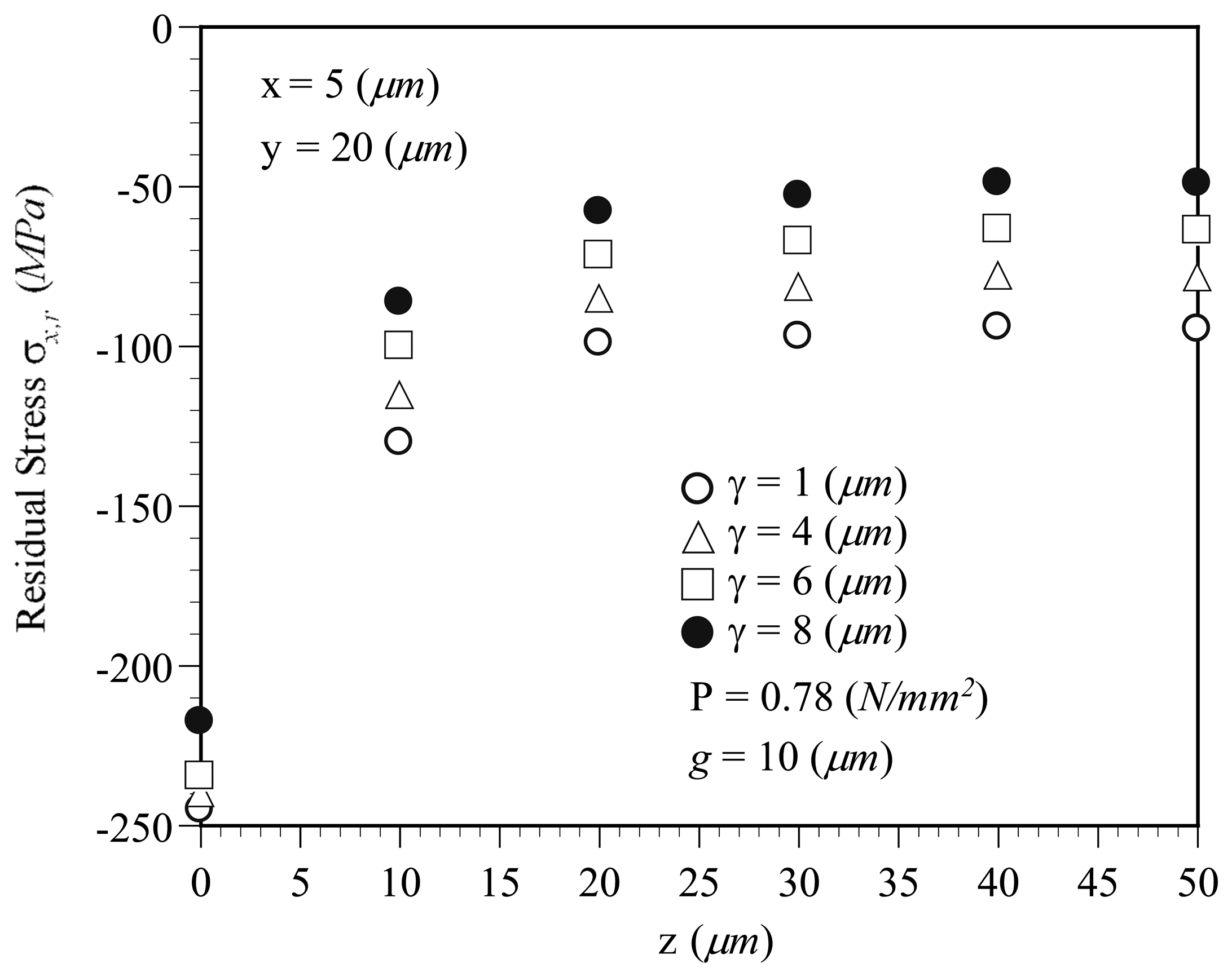
The effect of plating film thickness on the residual stress σx,r distribution along the z-axis is shown in Figure 7. In this case, the contact gap and the electromagnetic force are g=10 μm and P = 0.78 N / mm2, respectively. It is obvious that the residual stress σx,r is affected significantly by the film thickness. A larger film thickness results in a smaller compressive residual stress in the microcantilever beam. The contact location of the microcantilever beam and the electrode is affected by the contact gap as shown in Figure 8. The film thickness and the electromagnetic force used in this case are 6 μm and 10 mN, respectively. A load current of 100 mA is taken to emphasize the phenomenon of electrical contact. Figure 8 presents the electric current density distribution on the contact area for various contact gaps. The unit of the electric current density is mA / mm2. The microcantilever beam and the electrode do not contact at the free end for a small contact gap g=1 μm, as shown in Figure 8 (a). However, as the contact gap increases, the contact location moves gradually toward the free end of the beam. It can be observed that the maximum contact area occurs in the case of g=5 μm. The relationship between the contact reactive force and the contact gap is shown in Figure 9. It shows that the contact force decreases as the contact gap increases. Since the directions of the contact force and the magnetic actuating force are mutually opposite, a larger contact force leads to a larger reverse stress. This explains why a smaller contact gap results in a smaller compressive residual stress, as shown in Figure 7.
In addition, the variations in contact location and contact force induced by the variation of contact gap change the size of the contact area. As presented above, in this case, the maximum contact area occurs when the contact gap g is 5 μm. Therefore, the smallest contact resistance is obtained for the microrelay when the contact gap g is 5 μm. Figure 10 presents the variation in maximum contact resistance at the microcantilever-electrode contact area for four different contact gaps. It can be concluded that contact behaviors, such as the contact area, contact resistance and current density, are affected significantly by the contact gap. In this study, the microrelay with a contact gap of g=5 μm gives the smallest contact resistance. A smaller contact resistance produces less heat when an electrical current conducts and thus can have a smaller temperature rise in a microrelay.
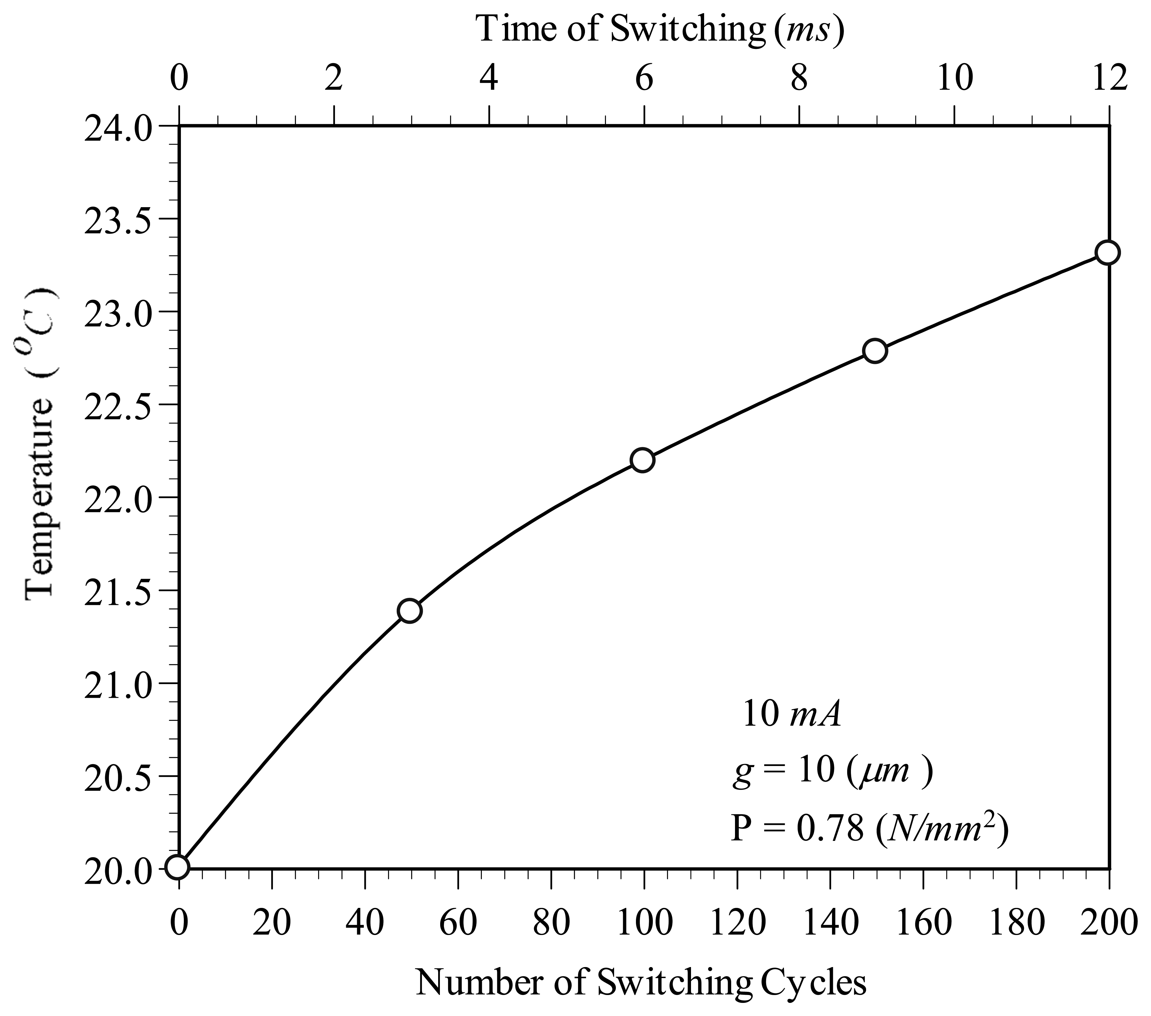
Figure 11 shows the variation in switching time used in the thermal-electrical coupling finite element simulation. In this figure, the amplitude “1” and “0” indicate the ON and OFF states, respectively. The switch contact time is 15 μs and the dwell time is 35 μs. The transition time between ON and OFF states is 5 μs. Figure 12 presents the distribution of the residual stress σx,r on the top surface of the microcantilever beam, i.e. y=20 μm and x=5 μm, along the z-axis for various switching cycles, i.e. Nc=1, 50, 100, 150 and 200. In this case, the contact gap, film thickness and electromagnetic force are taken as 10 μm, 6 μm and 0.78 N / mm2, respectively. It can be obtained that the compressive residual stress increases with increasing switching cycles. This can be attributed to the plasticity occurs on the top surface near the fixed support end of the cantilever beam. As the number of switching cycles increases, the amount of plasticity accumulates and the residual stress increases. A larger residual stress remains in the microcantilever beam can decrease the lifecycle of the beam. The accumulation of plasticity also makes the variation in vertical displacement at the free end increase, as shown in Figure 13. Figure 13 illustrates the variation in vertical displacement for various switching cycles at the free end on the bottom of the microcantilever beam, i.e. x=600, y=-6 and z=0 μm. It is observed that the vertical displacement increases as the switching cycle increases. A larger displacement at the microcantilever tip results in a gap with a smaller distance between the microcantilever beam and the electrode. This displacement change also changes the microcantilever-electrode contact location. Also, as discussed above, the decrease of the distance between the microcantilever beam and the electrode increases the contact reaction force. The augmented contact reaction force increases the reverse bending stress, i.e. the compressive bending stress, gradually. This is why the compressive residual stress accumulates when the number of switching cycles increases, as it can be seen in Figure 12. Figure 14 shows the effect of switching cycles on the maximum contact temperature rise. In this case, the contact gap, film thickness, electromagnetic force and contact current are taken as 10 μm, 6 μm, 0.78 N / mm2 and 10 mA, respectively. The results indicate that the temperature rise increases with increasing switching cycles. The temperature rise is about 3 °C after 200 times of continual contact. In case of the contact current is less than 10 mA, the effect of switching cycles on the temperature rise is not obvious. Thus, the thermal-electrical coupling in the finite element model can be neglected in the simulation.
5. Conclusions
This study has investigated the electrical contact and the residual stress of a microrelay using a three-dimensional elastic-plastic finite element model. A model with thermal-electrical coupling and thermal-stress coupling is used in finite element analysis. The effects of contact gap, plating film thickness and number of switching cycles on the contact residual stress, contact force, plastic deformation, and contact temperature of the microrelay switch are explored. Based upon the current simulation results, the following conclusions can be drawn:
- The residual stress is affected significantly by the contact gap and the film thickness. The residual stress increases with the increase of the contact gap and decreases as the film thickness increases.
- A smaller contact gap results in a larger microcantilever-electrode contact force. The contact location of the microcantilever beam and the electrode is varied with the size of the contact gap. The contact location is moved toward the free end of microcantilever beam as the contact gap increases.
- The residual stress increases as the number of switching cycles increases. A larger residual stress remains in the microcantilever beam can decrease the lifecycle of microrelay.
- The plastic deformation at the microcantilever tip increases as the number of switching cycles increases. This plastic deformation at the microcantilever tip decreases the gap distance between the microcantilever beam and the electrode, and changes the microcantilever-electrode contact location as well.
References and Notes
- Hosaka, H.; Kuwano, H.; Yanagisawa, K. Electromagnetic Microrelays: Concepts and Fundamental Characteristics. Proc. IEEE Microelectromechanical Sys. Conf. 1993; pp. 12–17. [Google Scholar]
- Schimkat, J. Contact Measurements Providing Basic Design Data for Microrelay. Sensors and Actuators A: Physical 1999, 73, 138–143. [Google Scholar]
- Holm, R. Electric Contacts, Theory and Applications; Springer-Verlag: New York, 1967. [Google Scholar]
- Li, D.; Zhang, Y. Finite Element Simulation and Theoretical Analysis of Microelectromechanical System Relays. Proc. Int. Conf. on MEMS, NANO and Smart Systems; 2003. [Google Scholar]
- Norgerg, G.; Dejanovic, S.; Hesselbom, H. Contact Resistance of Thin Metal Film Contacts. IEEE Trans. Components and Packaging Technologies 2006, 29, 371–378. [Google Scholar]
- Lee, C. Y.; Tsai, C. H.; Chen, L. W.; Fu, L. M.; Chen, Y. C. Elastic-Plastic Modeling of Heat-Treated Bimorph Micro-Cantilevers. Journal of Microsystem Technologies 2006, 979–986. [Google Scholar]
- Gere, J. M.; Timoshenko, S. P. Mechanics of Materials; Stanley Thornes: United Kingdom, 1999; Chapter 6; pp. 391–455. [Google Scholar]
- Hatafuku, H.; Sarudate, C.; Konno, A. Estimation of Residual Stresses in Magnetic Metals by Using Ultrasonic Method. IEEE Trans. Magn. 2002, 3309–3311. [Google Scholar]
Figure 1.
Geometrical configuration of the microrelay switch.
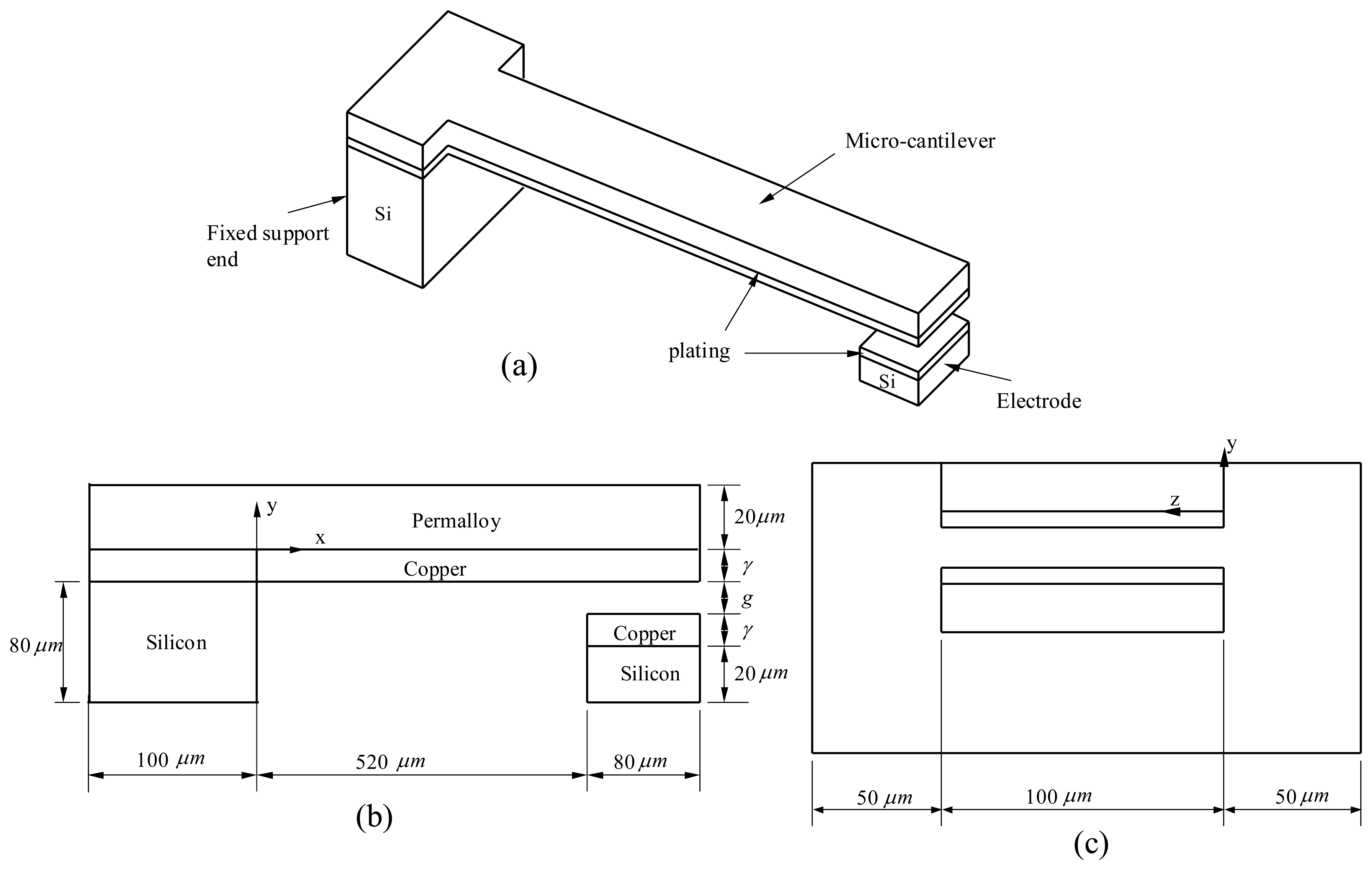
Figure 2.
Schematic illustration of the contact load and the cross section of the microrelay.

Figure 3.
Typical finite element model.
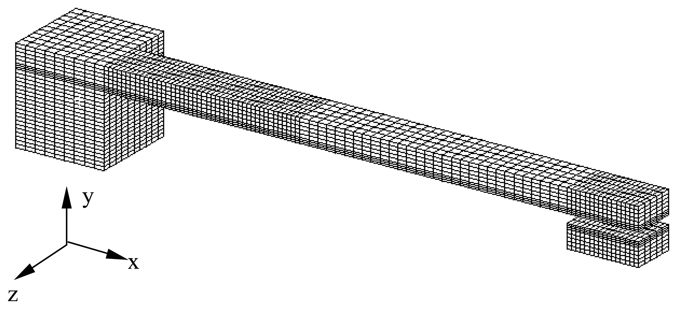
Figure 4.
Variation of maximum tensile bending stress σx,max(tensile) at fixed end for various plating film thicknesses.
Figure 4.
Variation of maximum tensile bending stress σx,max(tensile) at fixed end for various plating film thicknesses.
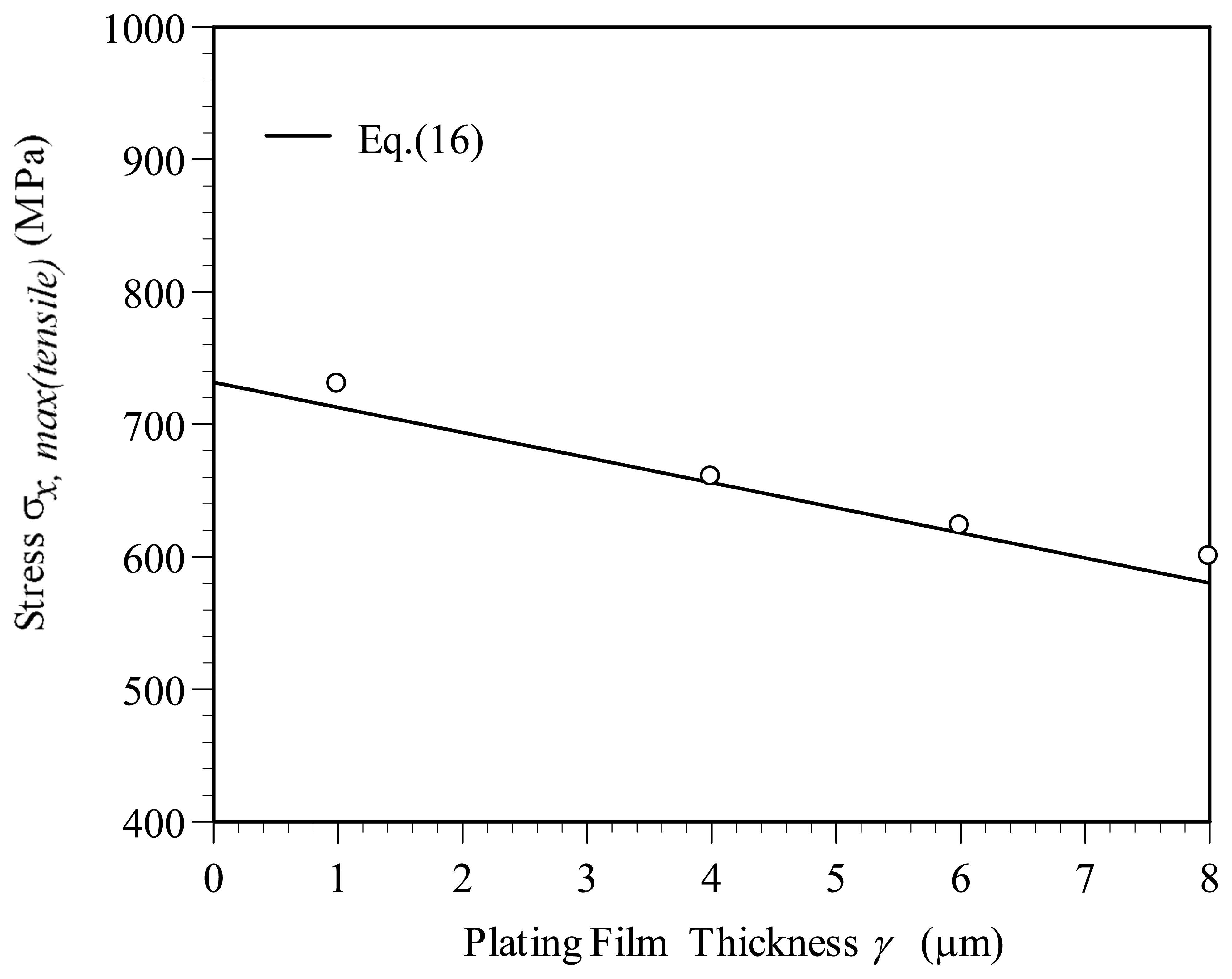
Figure 5.
Bending stress σx distribution on the top surface of the microcantilever beam.
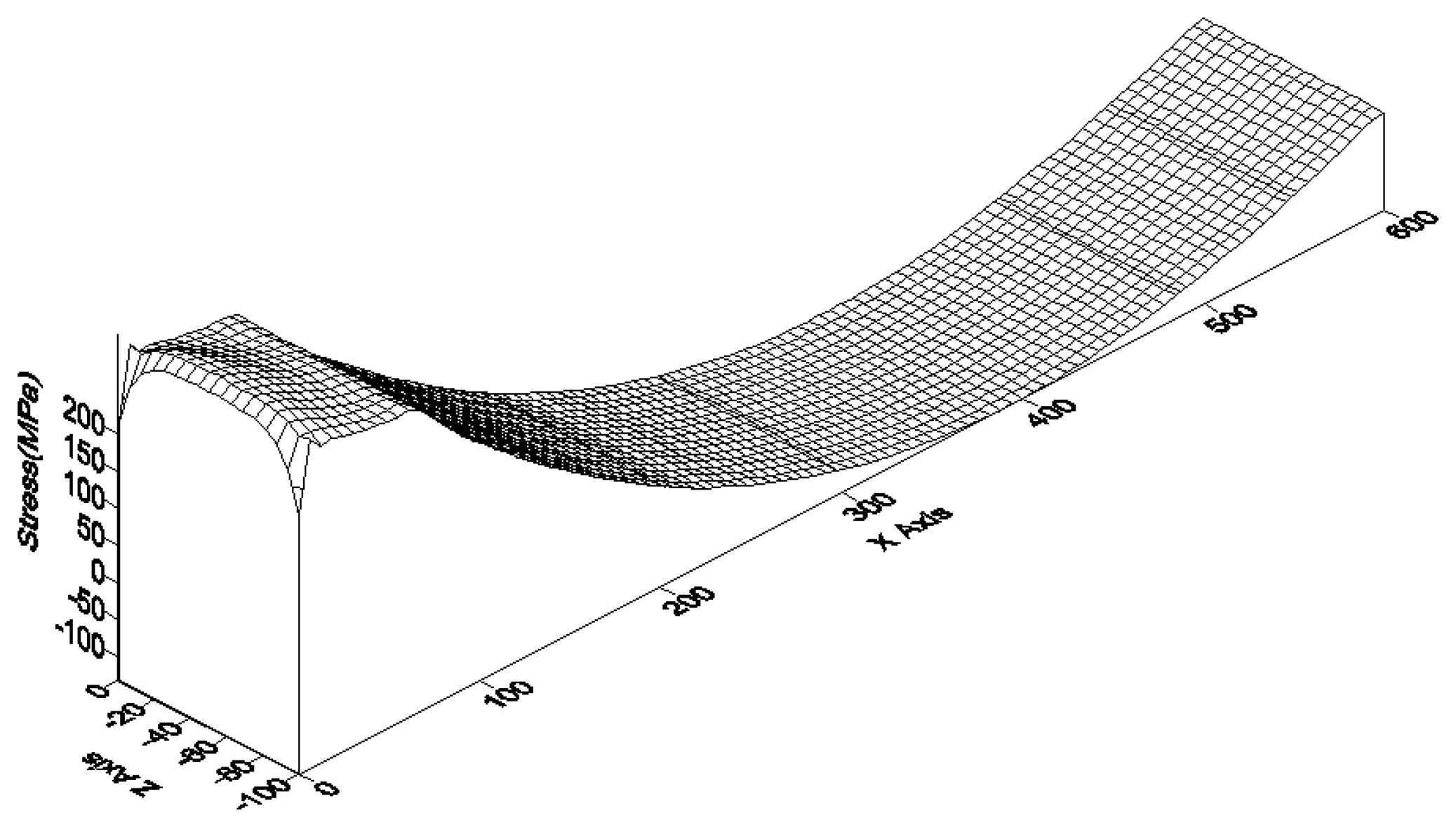
Figure 6.
Residual stress σx,r distribution on the top surface of the microcantilever beam along the z-axis for various contact gaps.
Figure 6.
Residual stress σx,r distribution on the top surface of the microcantilever beam along the z-axis for various contact gaps.
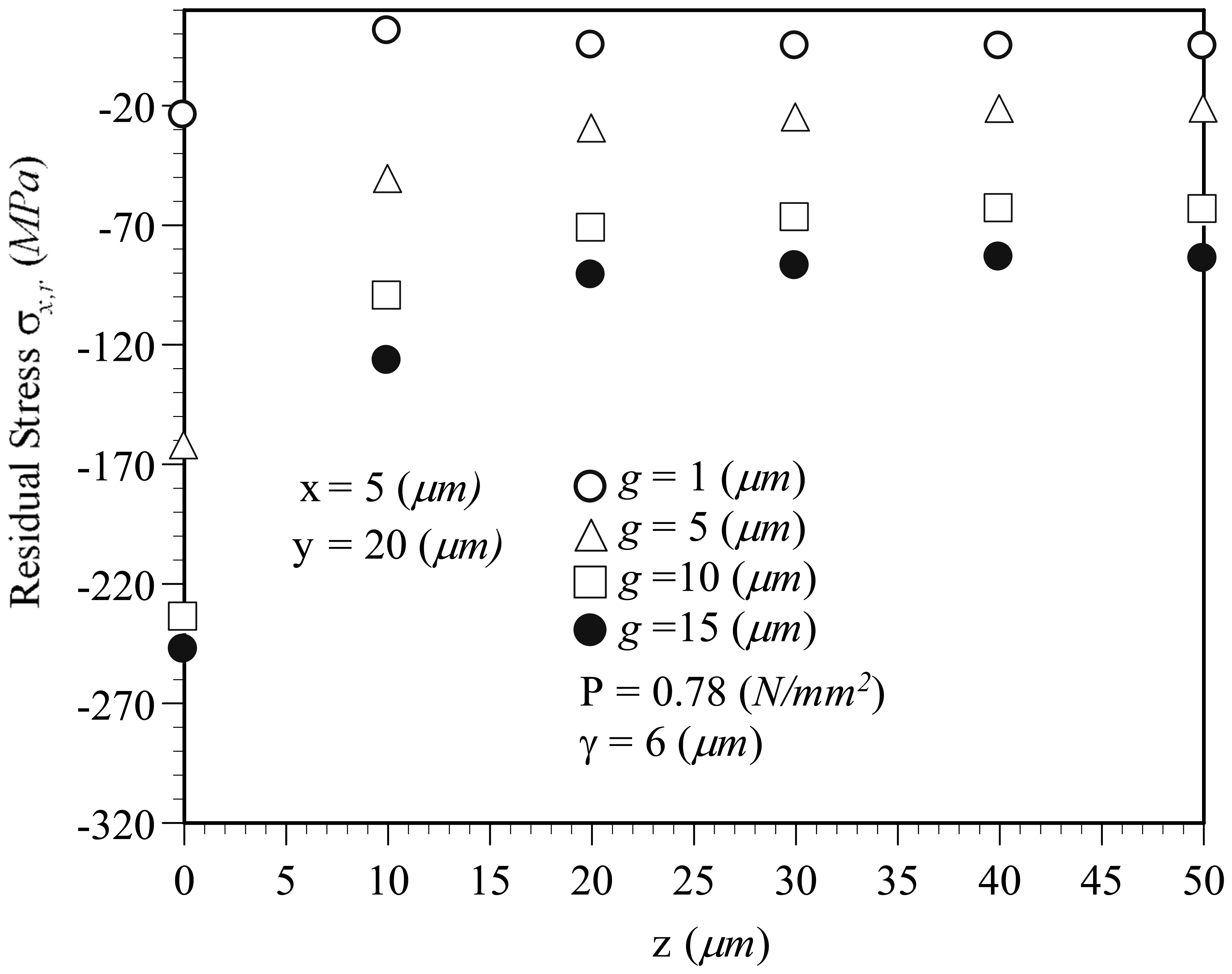
Figure 7.
Residual stress σx,r distribution on the top surface of the microcantilever beam along the z-axis for various film thicknesses.
Figure 7.
Residual stress σx,r distribution on the top surface of the microcantilever beam along the z-axis for various film thicknesses.

Figure 8.
The electric current density distribution on the contact area for various contact gaps.
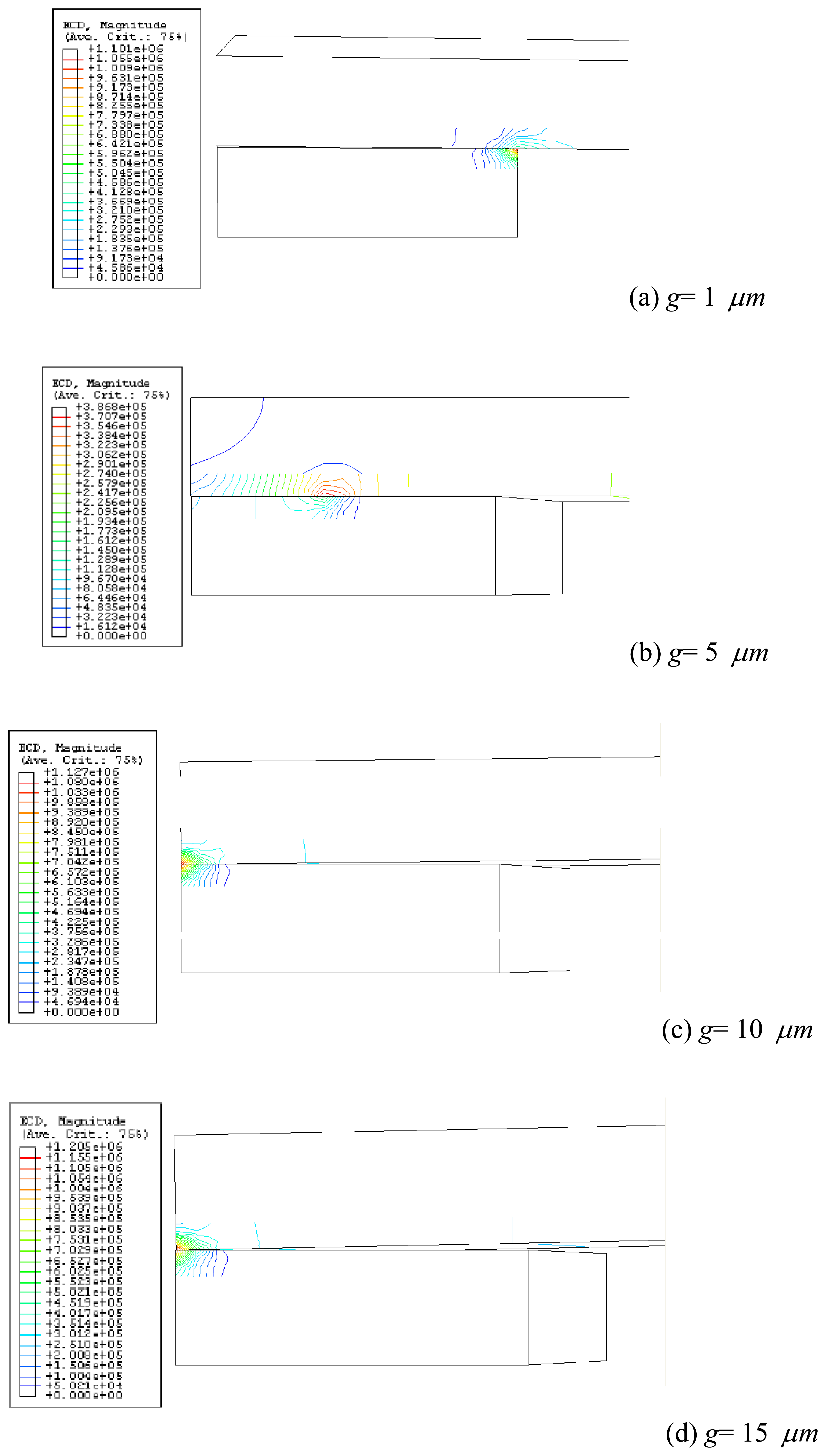
Figure 9.
Contact reactive force as a function of the contact gap.
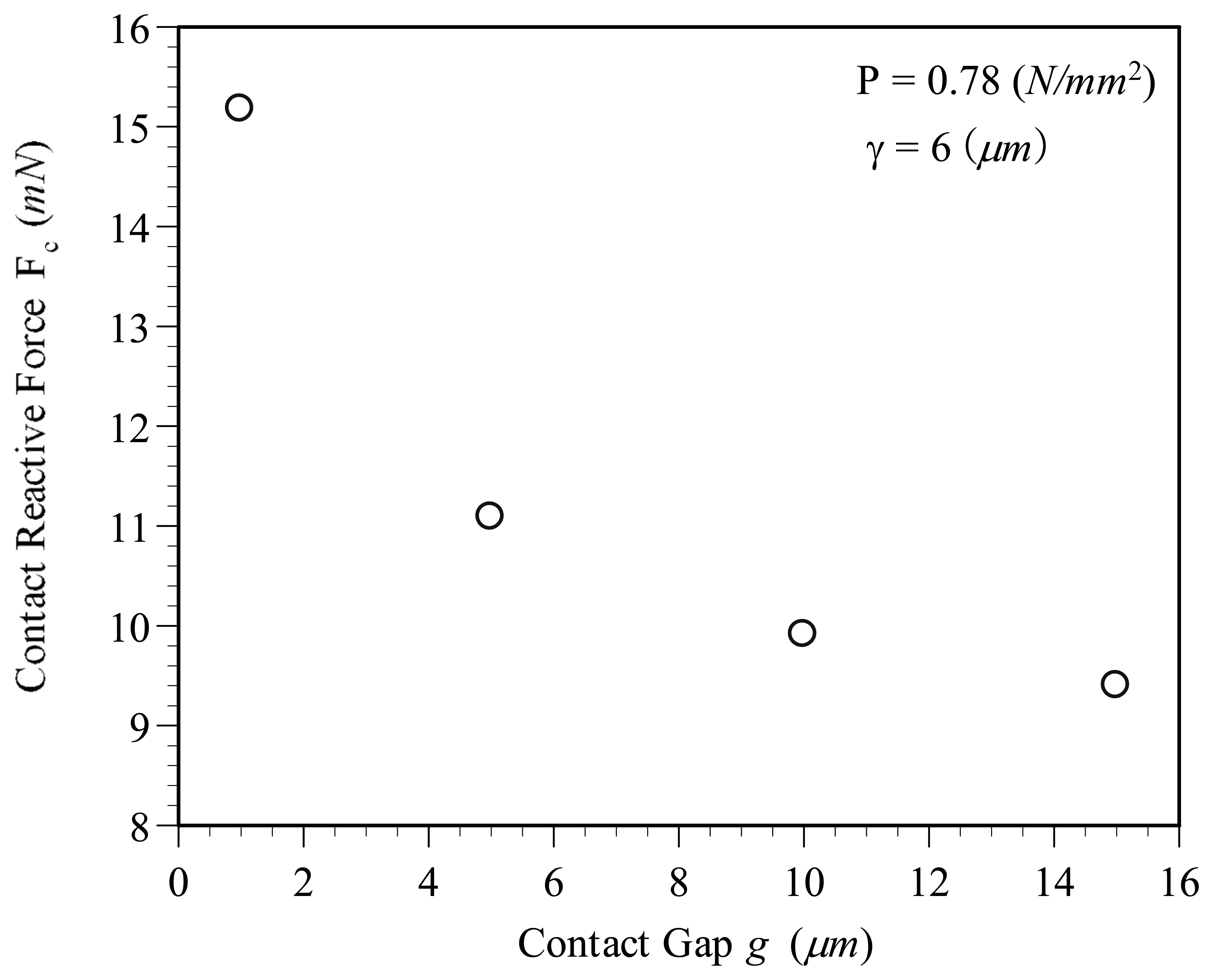
Figure 10.
Variation in maximum contact resistance at the microcantilever-electrode contact area for various contact gaps.
Figure 10.
Variation in maximum contact resistance at the microcantilever-electrode contact area for various contact gaps.
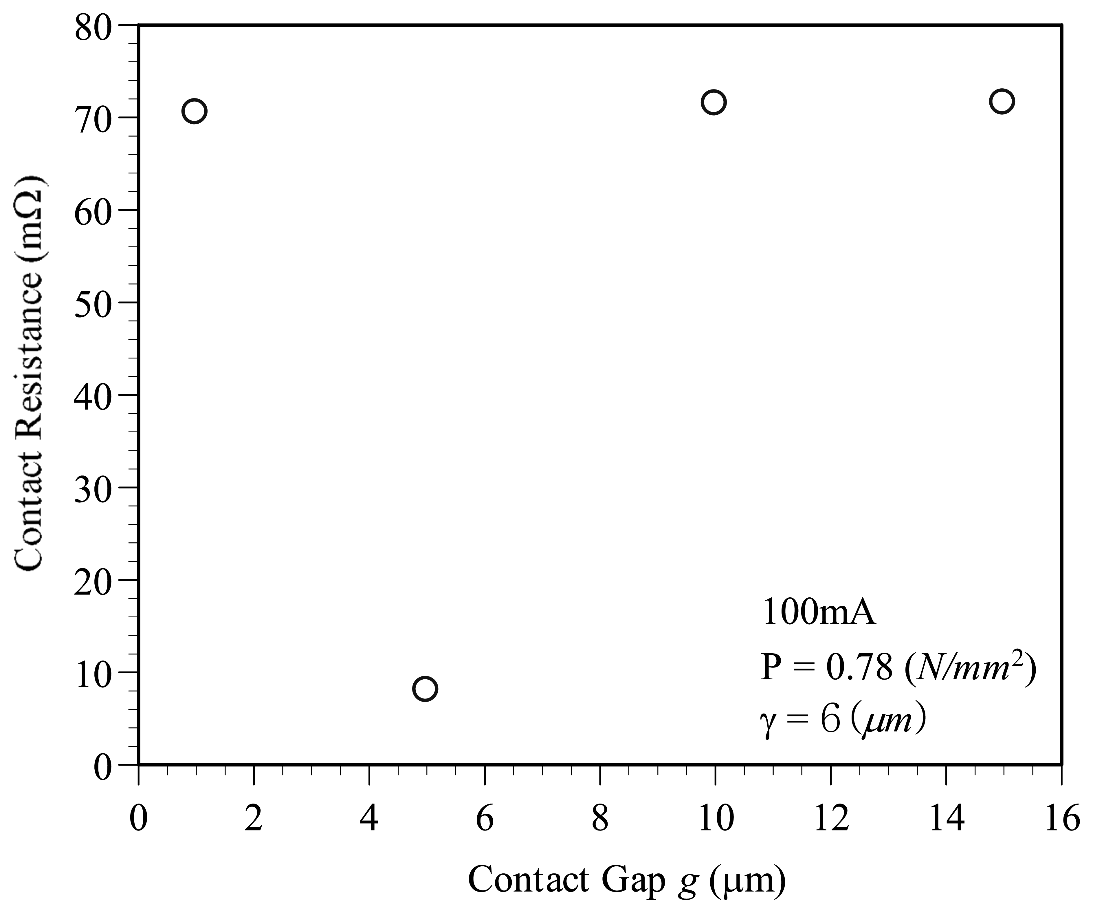
Figure 11.
Variation in switching time used in the thermal-electrical coupling finite element simulation.
Figure 11.
Variation in switching time used in the thermal-electrical coupling finite element simulation.
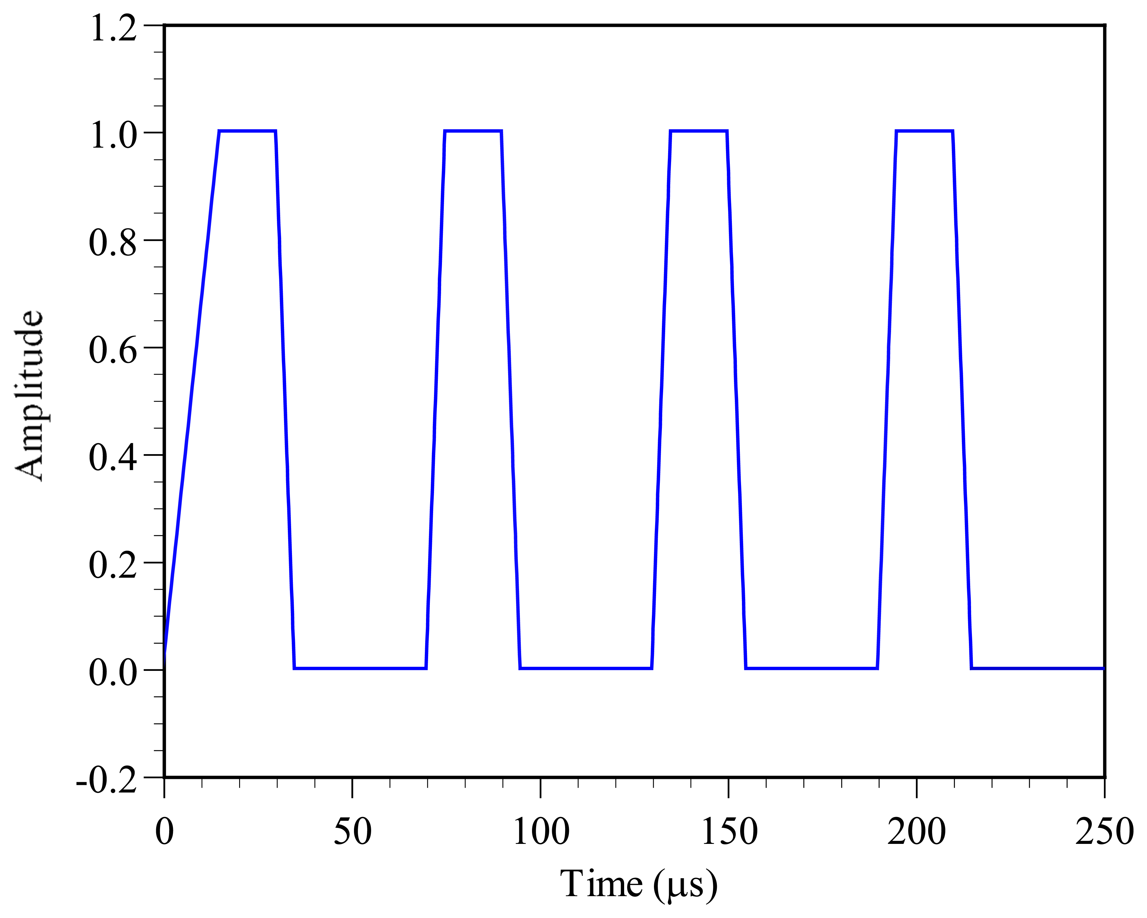
Figure 12.
Distribution of residual stress σx,r on the top surface of the microcantilever beam along the z-axis for various switching cycles.
Figure 12.
Distribution of residual stress σx,r on the top surface of the microcantilever beam along the z-axis for various switching cycles.
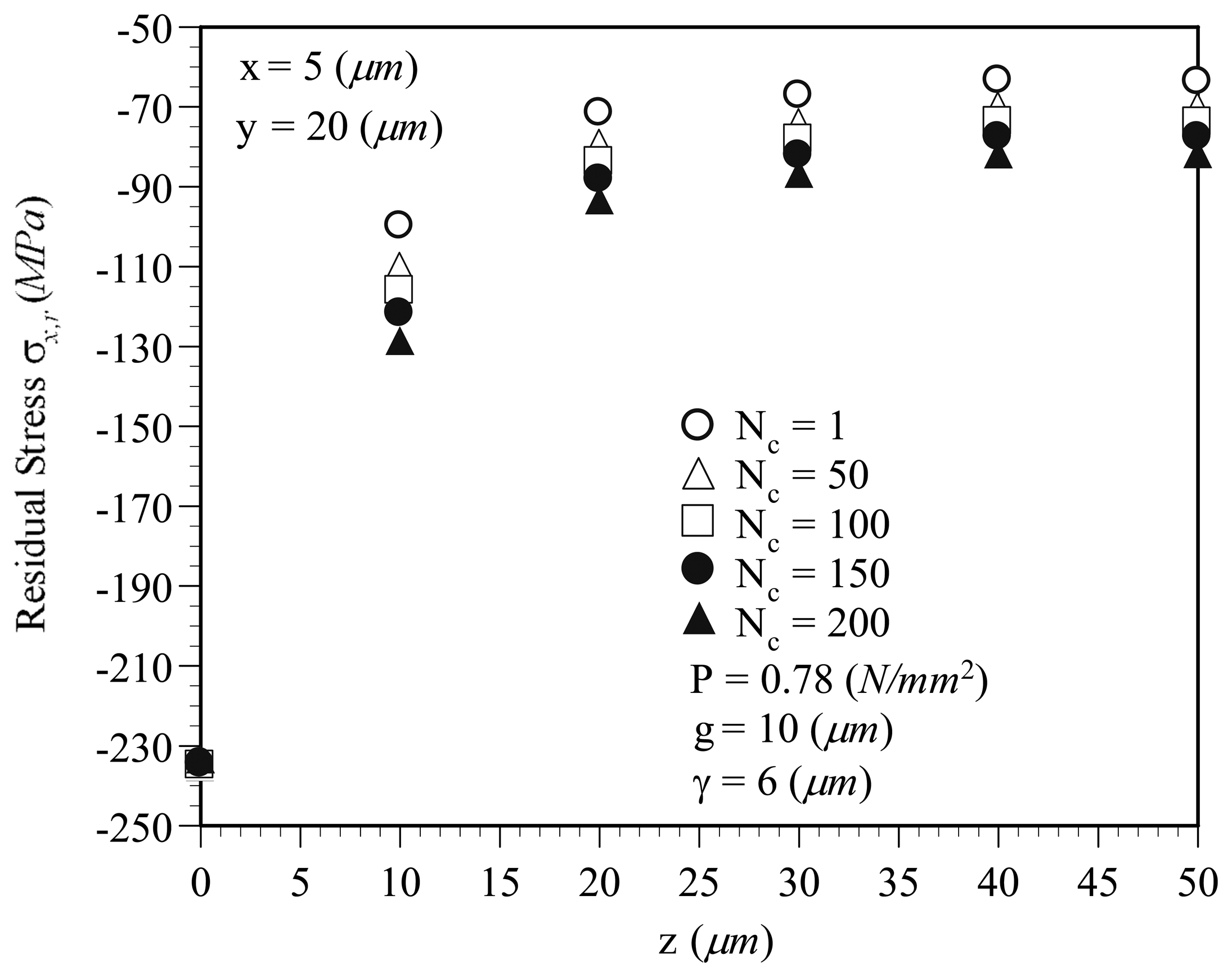
Figure 13.
Variation in vertical displacement for various switching cycles at the free end.
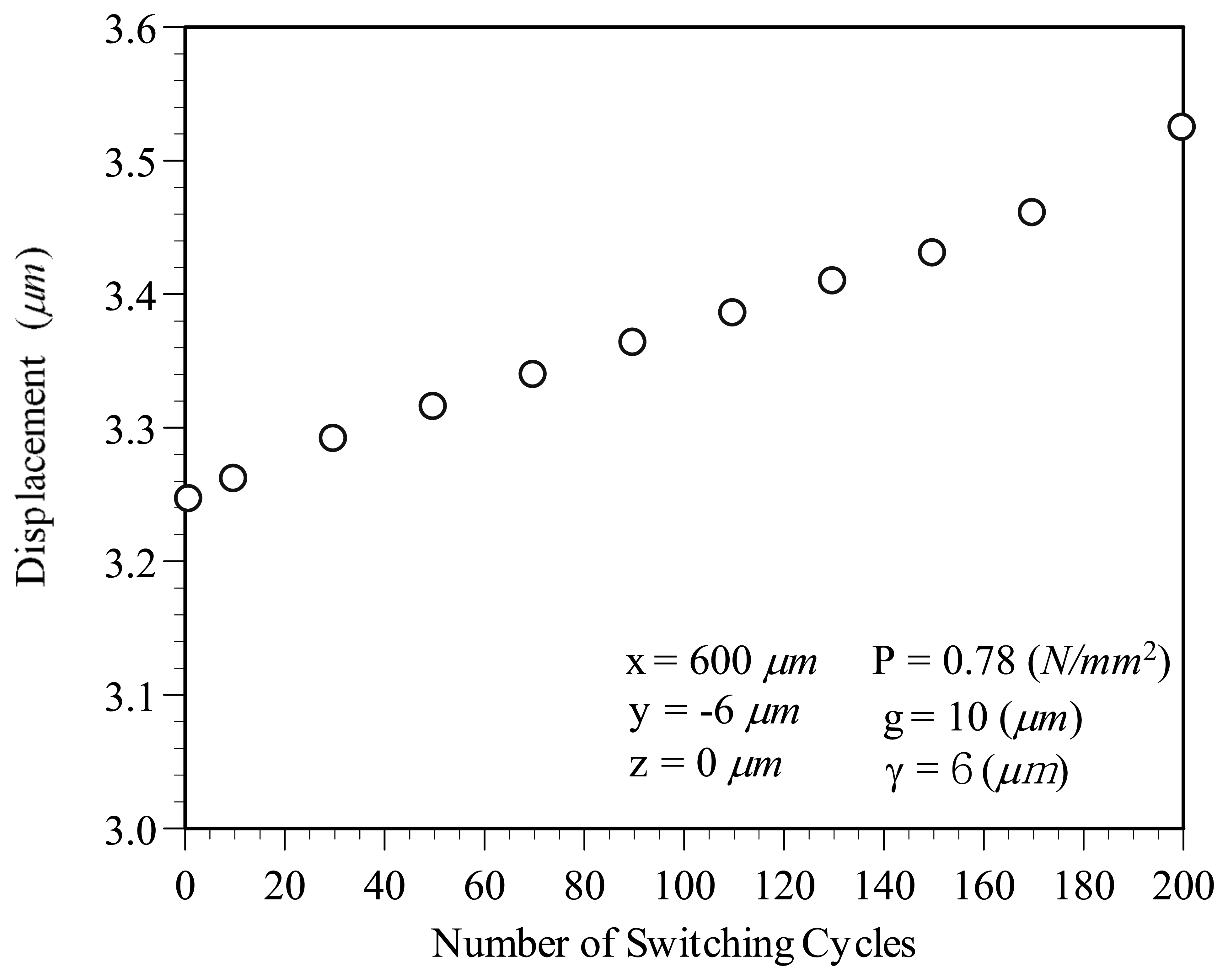
Figure 14.
Effect of switching numbers on the maximum contact temperature rise.

| Permalloy | Copper | Silicon | |
|---|---|---|---|
| Young's modulus (GPa) | 255 | 120 | 73 |
| Poission's ratio | 0.3 | 0.35 | 0.26 |
| Yielding strength (MPa) | 280 [8] | 127 | – |
| Ultimate strength (MPa) | 568 [8] | 435 | 180 |
| Coefficient of Expansion (°C)−1 | 13.347 E-6 | 16.483 E-6 | 3.0 E-6 |
| Conductivity (W / m·K) | 49.99 | 386.52 | 71 |
| Conductance (1 / Ω·m) | 6.249 E+6 | 58.06 E+6 | 60 E+6 |
| Density (kg / m3) | 9200 | 8935 | 3100 |
| Specific Heat (J / kg·K) | 419.99 | 383.62 | 710 |
© 2007 by MDPI ( http://www.mdpi.org). Reproduction is permitted for noncommercial purposes.
Share and Cite
MDPI and ACS Style
Chen, Y.-C.; Tsai, H.-H.; Lu, W.-H.; Chen, L.-W. Effect of Electrical Contact on the Contact Residual Stress of a Microrelay Switch. Sensors 2007, 7, 2997-3011. https://doi.org/10.3390/s7112997
AMA Style
Chen Y-C, Tsai H-H, Lu W-H, Chen L-W. Effect of Electrical Contact on the Contact Residual Stress of a Microrelay Switch. Sensors. 2007; 7(11):2997-3011. https://doi.org/10.3390/s7112997
Chicago/Turabian StyleChen, Yung-Chuan, Hsun-Heng Tsai, Wei-Hua Lu, and Li-Wen Chen. 2007. "Effect of Electrical Contact on the Contact Residual Stress of a Microrelay Switch" Sensors 7, no. 11: 2997-3011. https://doi.org/10.3390/s7112997