
A 3D Faraday Shield for Interdigitated Dielectrometry Sensors and Its Effect on Capacitance


Abstract
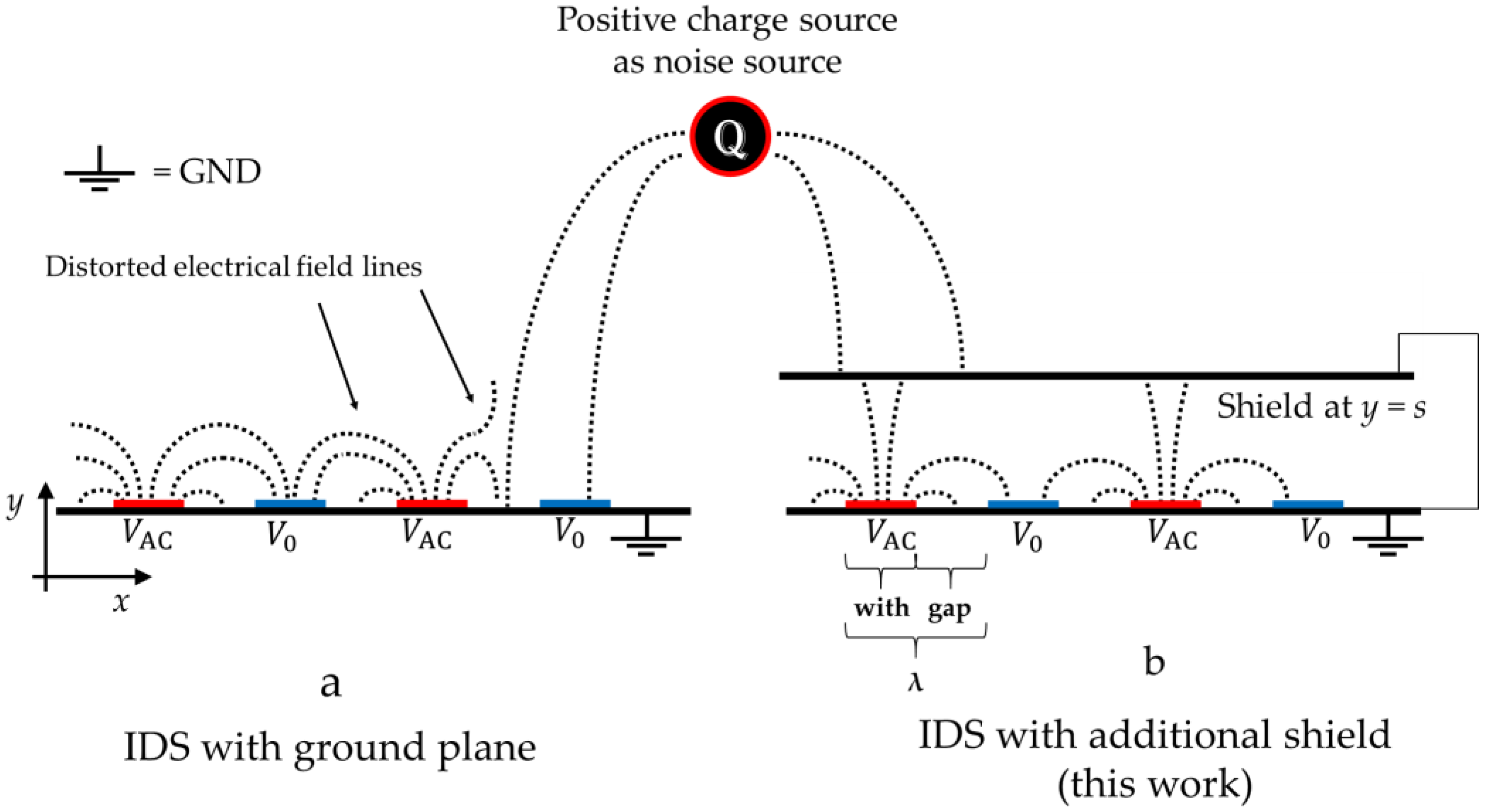
:1. Introduction
2. Materials and Methods
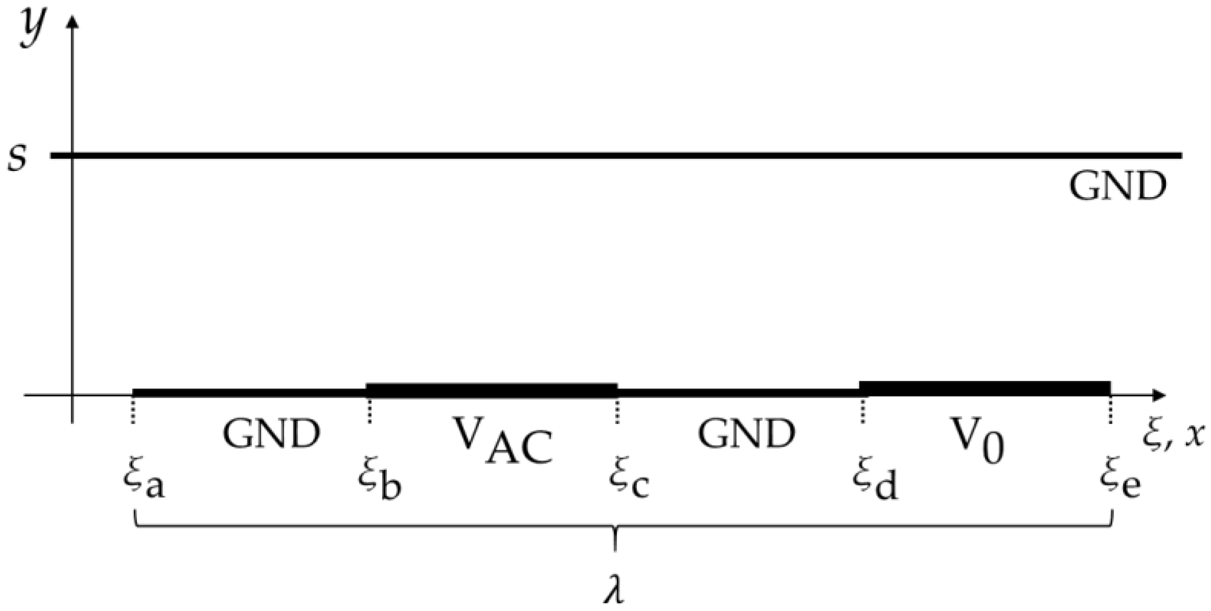
2.1. Theoretical Approach via Green’s Function
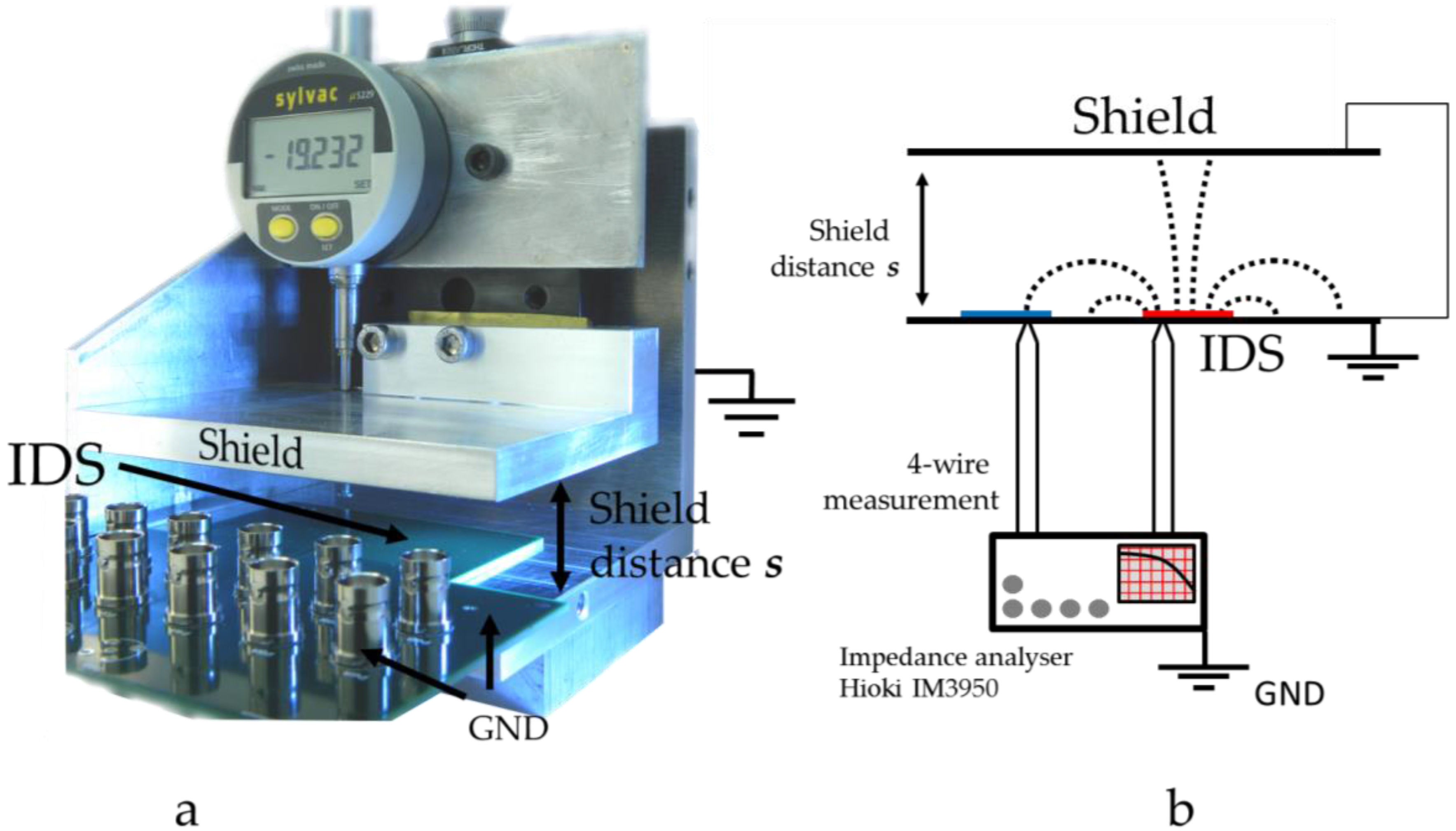
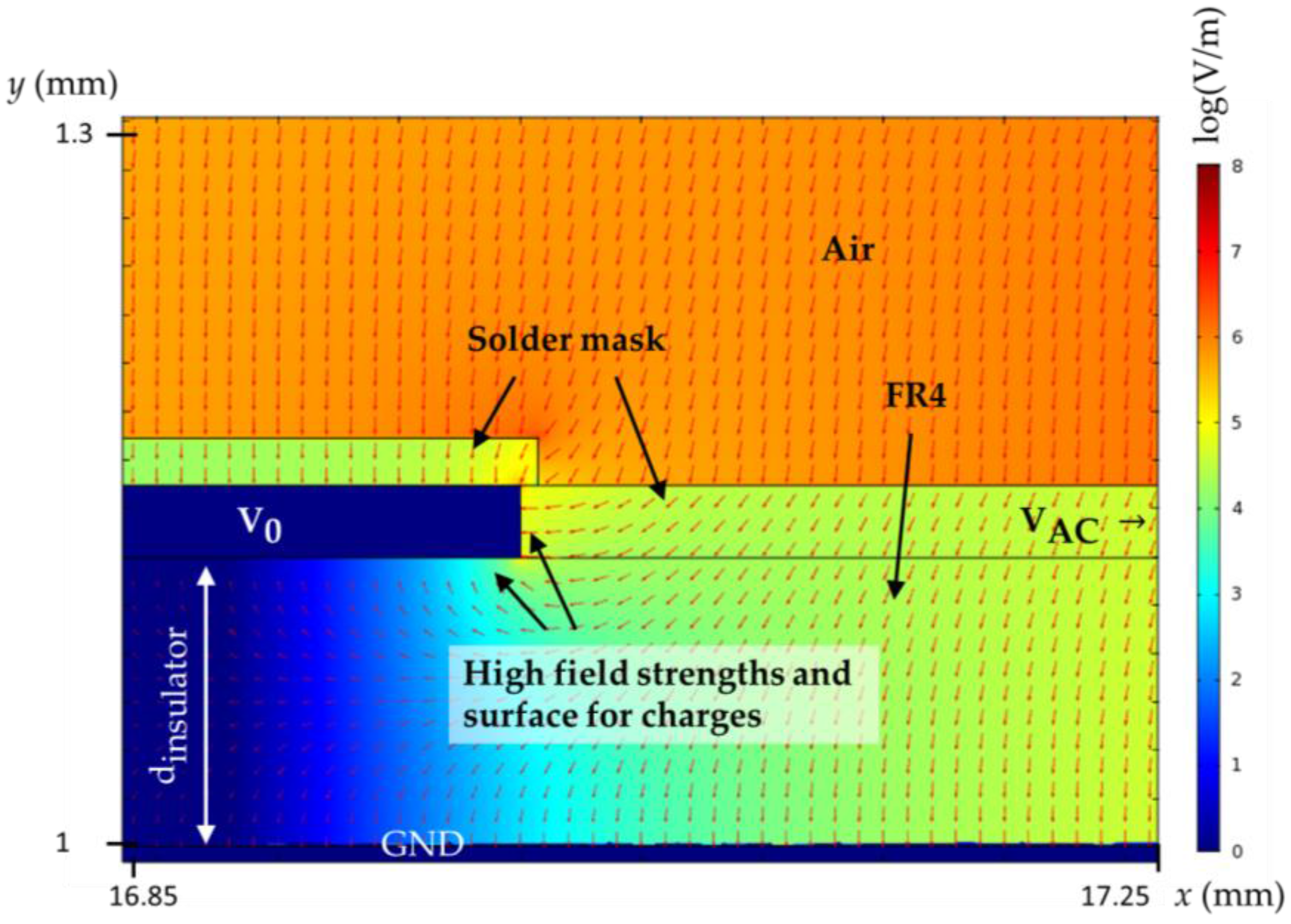
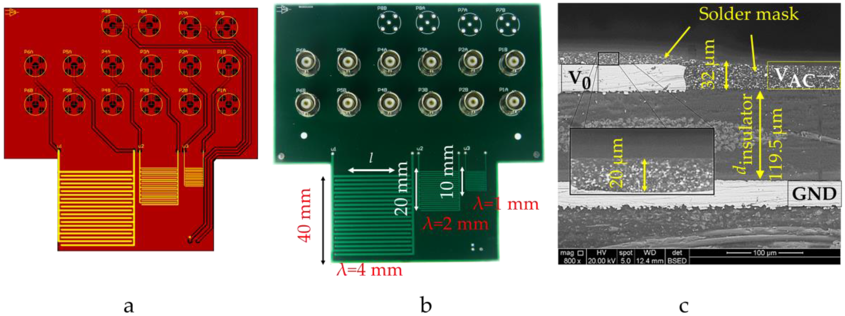
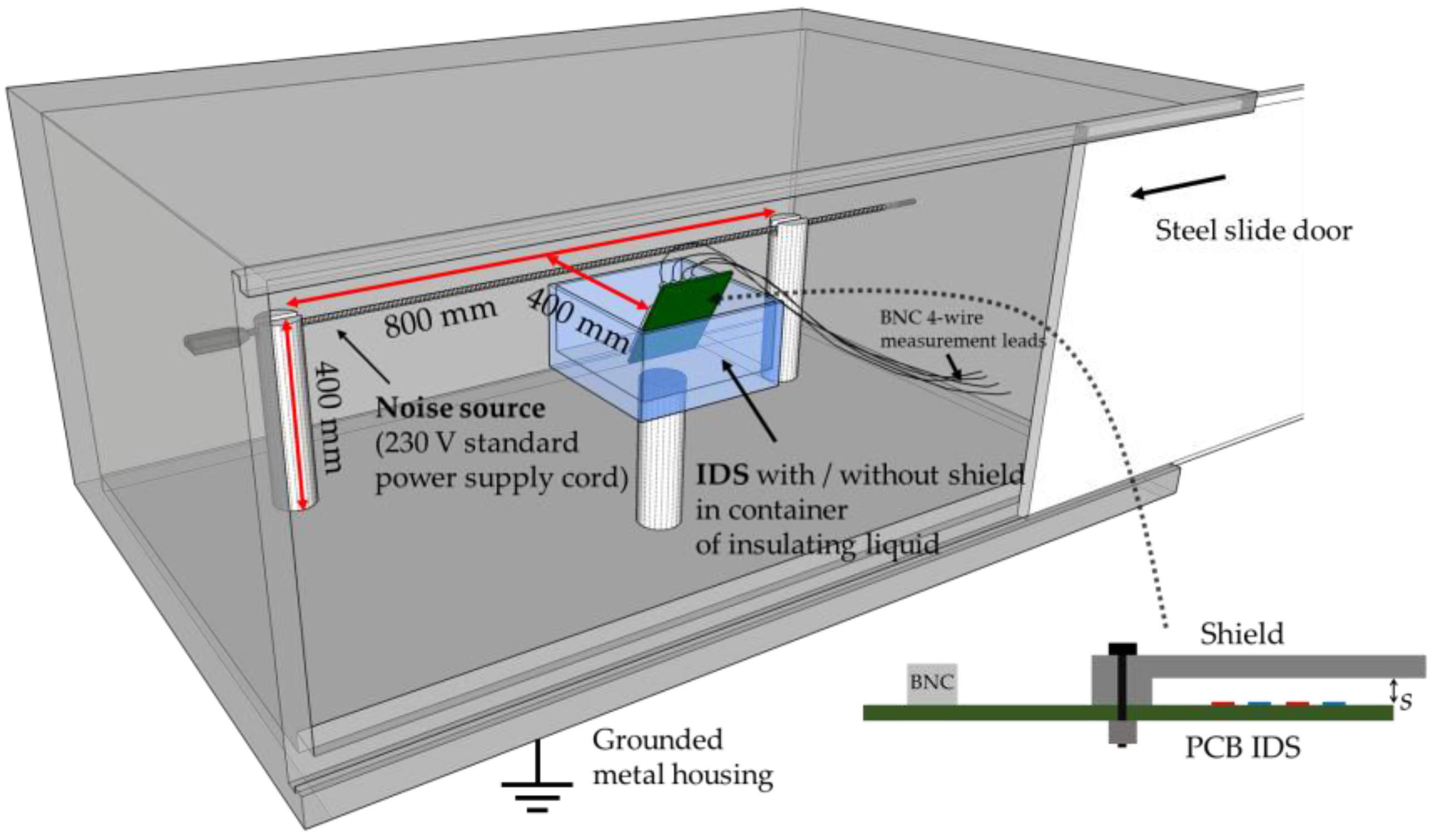
2.2. Experimental Setup and Used IDS
3. Results
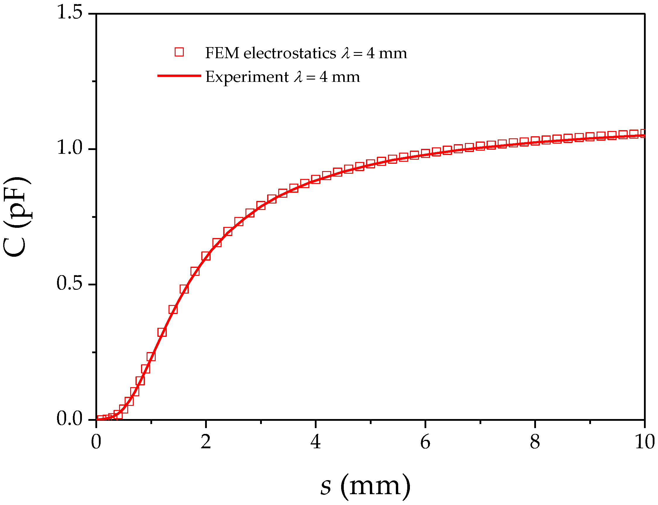
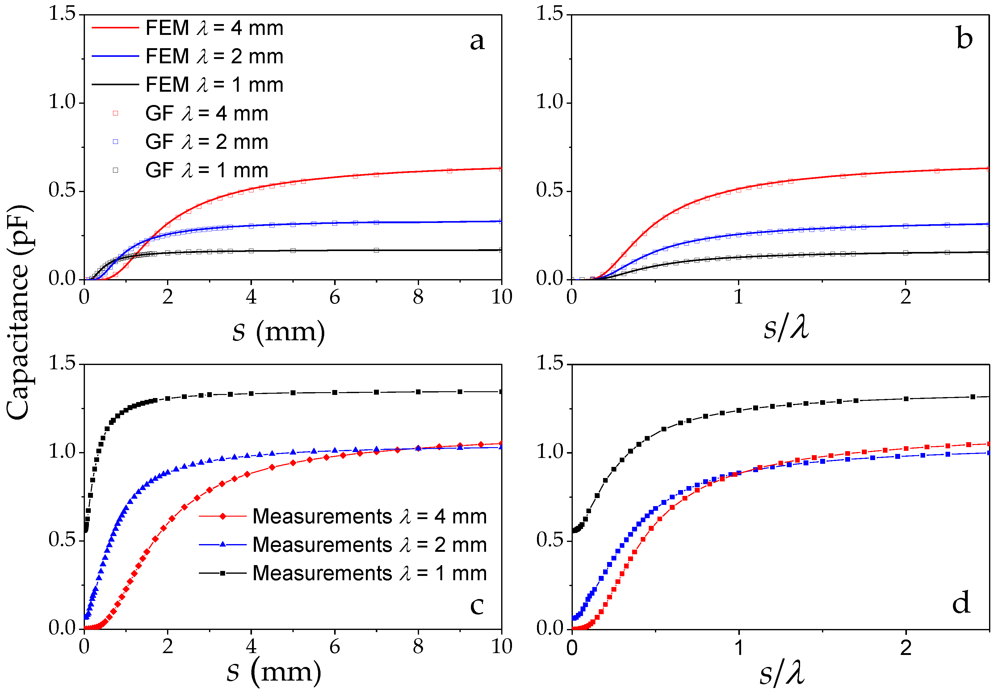
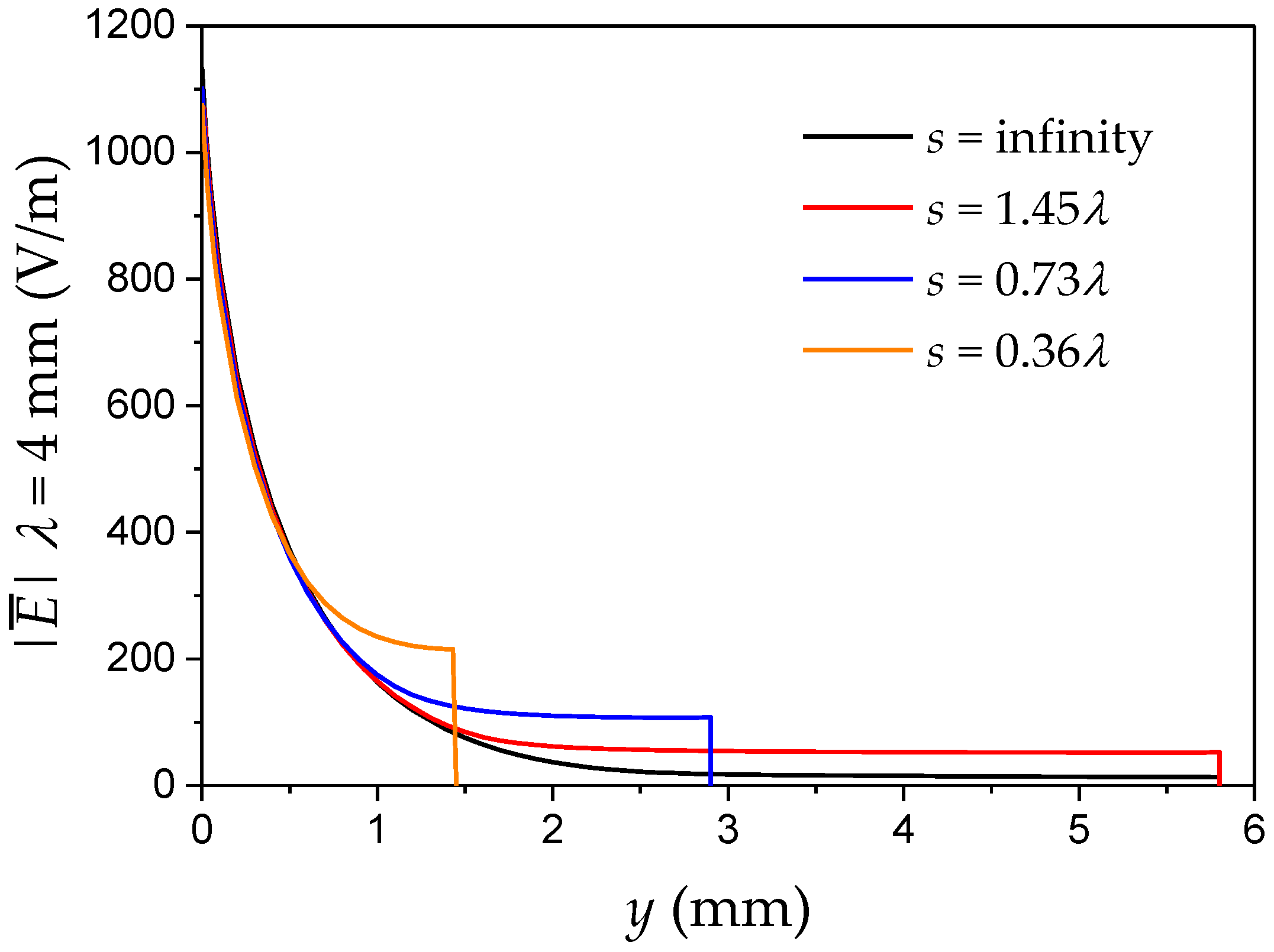
3.1. Capacitance with Shield Distance
3.2. Choosing a Shield Distance
3.3. Difference Between Experiment and Theory
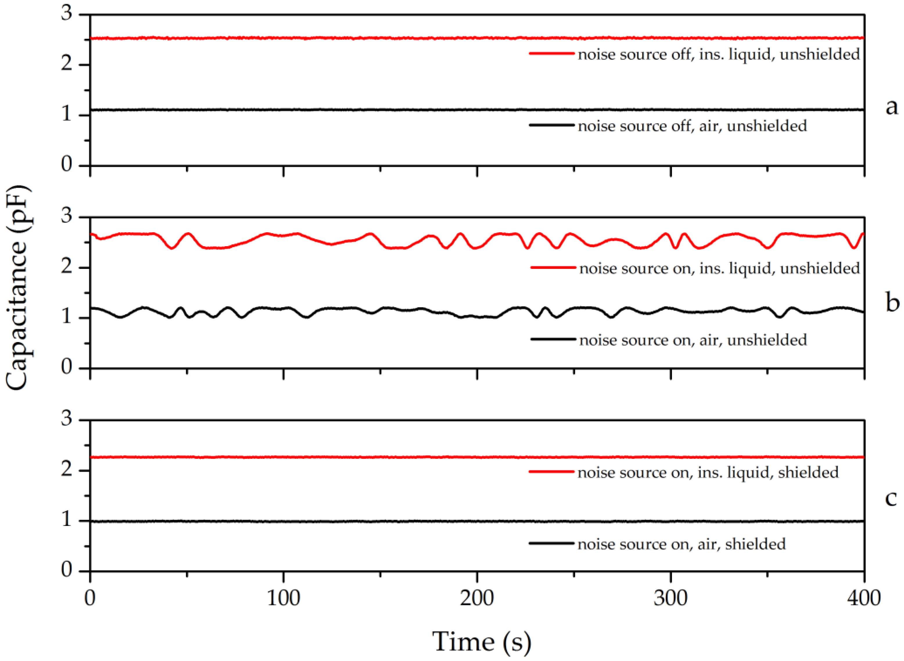
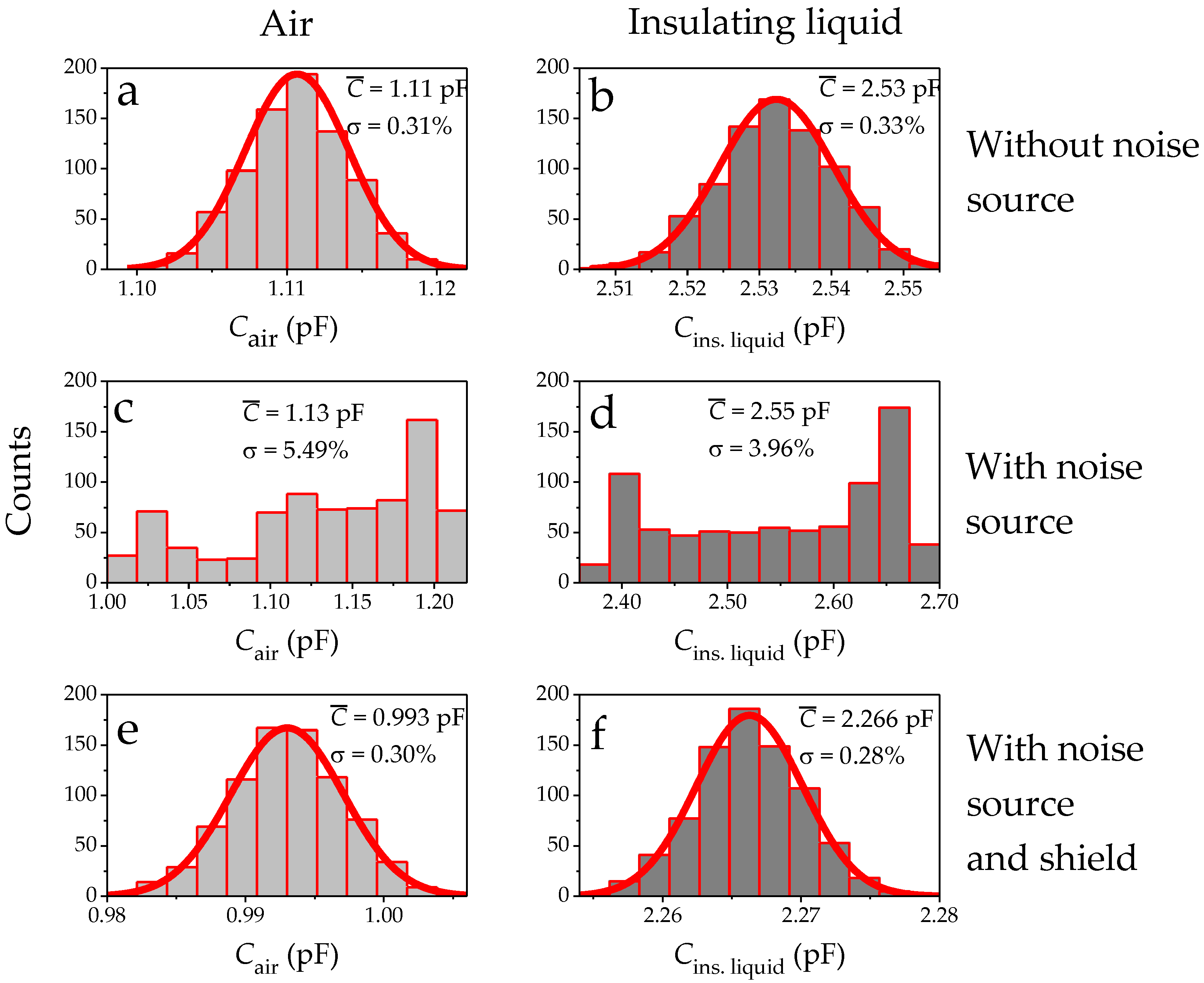
3.4. Validation Test of Shield’s Impact on Noise Reduction
4. Summary and Conclusions
Acknowledgments
Author Contributions
Conflicts of Interest
References
- Fofana, I. 50 years in the development of insulating liquids. IEEE Electr. Insul. Mag. 2013, 29, 13–25. [Google Scholar] [CrossRef]
- Rafiq, M.; Lv, Y.Z.; Zhou, Y.; Ma, K.B.; Wang, W.; Li, C.R.; Wang, Q. Use of vegetable oils as transformer oils—A review. Renew. Sustain. Energy Rev. 2015, 52, 308–324. Available online: http://www.sciencedirect.com/science/article/pii/S1364032115006796 (accessed on 5 June 2016). [Google Scholar] [CrossRef]
- Rouse, T.O. Mineral insulating oil in transformers. IEEE Electr. Insul. Mag. 1998, 14, 6–16. [Google Scholar] [CrossRef]
- Yu, C.L.; Moore, R.A. Properties of alternately charged coplanar parallel strips by conformal mappings. IEEE Trans. Electr. Devices 1968, 15, 173–180. [Google Scholar] [CrossRef]
- Seaver, A.E.; Mamishev, A.V.; Du, Y.; Lesieutre, B.C.; Zahn, M. Development and applications of fringing electric field dielectrometry sensors and parameter estimation algorithms. J. Electr. 1999, 46, 109–123. Available online: http://www.sciencedirect.com/science/article/pii/S0304388699000066 (accessed on 6 Januanry 2016). [Google Scholar] [CrossRef]
- Cao, S.; Pyatt, S.; Anthony, C.; Kubba, A.; Kubba, A.; Olatunbosun, O. Flexible Bond Wire Capacitive Strain Sensor for Vehicle Tyres. Sensors 2016, 16, 929–946. Available online: https://www.mdpi.com/1424-8220/16/6/929 (accessed on 10 November 2016). [Google Scholar] [CrossRef] [PubMed]
- Khan, M.; Kang, S.-W. Highly Sensitive Temperature Sensors Based on Fiber-Optic PWM and Capacitance Variation Using Thermochromic Sensing Membrane. Sensors 2016, 16, 1064–1078. Available online: https://www.mdpi.com/1424-8220/16/7/1064 (accessed on 10 November 2016). [Google Scholar] [CrossRef] [PubMed]
- Mamishev, A.; Yanqing, D.; Zahn, M. Measurement of Dielectric Property Distributions Using Interdigital Dielectrometry Sensors. In Proceeding of the Conference on Electrical Insulation and Dielectric Phenomena, Virginia, VA, USA, 22–25 October 1995; pp. 309–312.
- Mamishev, A.V.; Cantrell, S.R.; Du, Y.; Lesieutre, B.C.; Zahn, M. Uncertainty in multiple penetration depth fringing electric field sensor measurements. IEEE Trans. Instrum. Meas. 2002, 51, 1192–1199. [Google Scholar] [CrossRef]
- Wang, H.; Chen, L.; Wang, J.; Sun, Q.; Zhao, Y. A Micro Oxygen Sensor Based on a Nano Sol-Gel TiO2 Thin Film. Sensors 2014, 14, 16423–16433. Available online: https://www.mdpi.com/1424-8220/14/9/16423 (accessed on 10 February 2016). [Google Scholar] [CrossRef] [PubMed]
- Fong, C.-F.; Dai, C.-L.; Wu, C.-C. Fabrication and Characterization of a Micro Methanol Sensor Using the CMOS-MEMS Technique. Sensors 2015, 15, 27047–27062. Available online: https://www.mdpi.com/1424-8220/15/10/27047 (accessed on 10 April 2016). [Google Scholar] [CrossRef] [PubMed]
- Khan, M.; Khalilian, A.; Kang, S.-W. Fast, Highly-Sensitive, and Wide-Dynamic-Range Interdigitated Capacitor Glucose Biosensor Using Solvatochromic Dye-Containing Sensing Membrane. Sensors 2016, 16, 265–278. Available online: https://www.mdpi.com/1424-8220/16/2/265 (accessed on 10 November 2016). [Google Scholar] [CrossRef] [PubMed]
- Khan, M.; Khalilian, A.; Kang, S.-W. A High Sensitivity IDC-Electronic Tongue Using Dielectric/Sensing Membranes with Solvatochromic Dyes. Sensors 2016, 16, 668–688. Available online: https://www.mdpi.com/1424-8220/16/5/668 (accessed on 10 November 2016). [Google Scholar] [CrossRef] [PubMed]
- Feng, J.; Kang, X.; Zuo, Q.; Yuan, C.; Wang, W.; Zhao, Y.; Zhu, L.; Lu, H.; Chen, J. Fabrication and Evaluation of a Graphene Oxide-Based Capacitive Humidity Sensor. Sensors 2016, 16, 314–323. Available online: https://www.mdpi.com/1424-8220/16/3/314 (accessed on 10 November 2016). [Google Scholar] [CrossRef] [PubMed]
- Xu, S.; Wang, P.; Dong, Y. Measuring Electrolyte Impedance and Noise Simultaneously by Triangular Waveform Voltage and Principal Component Analysis. Sensors 2016, 16, 576–591. Available online: https://www.mdpi.com/1424-8220/16/4/576 (accessed on 10 November 2016). [Google Scholar] [CrossRef] [PubMed]
- Standard Insulating Liquids Measurement of Relative Permittivity, Dielectric Dissipation Factor (tan δ) and d.c. Resistivity (IEC 60247:2004); British Standards Institution: London, UK, 2004; p. 27.
- Dervos, C.T.; Paraskevas, C.D.; Skafidas, P.; Vassiliou, P. Dielectric characterization of power transformer oils as a diagnostic life prediction method. IEEE Electr. Insul. Mag. 2005, 21, 11–19. [Google Scholar] [CrossRef]
- Jung, J.W.; Lim, Y.B.; Jung, J.S.; Yi, G.H.; Park, H.Y. The Analysis of Dielectric Characteristics of Transformer Oil Suffering Ageing Treatment. In Proceeding of the 2006 IEEE 8th International Conference on Properties & applications of Dielectric Materials, Bali, Indonesia, 26–30 June 2006; pp. 848–851.
- Li, X.B.; Larson, S.D.; Zyuzin, A.S.; Mamishev, A.V. Design principles for multichannel fringing electric field sensors. IEEE Sens. J. 2006, 6, 434–440. [Google Scholar] [CrossRef]
- Mamishev, A.V.; Sundara-Rajan, K.; Fumin, Y.; Yanqing, D.; Zahn, M. Interdigital sensors and transducers. Proc. IEEE 2004, 92, 808–845. [Google Scholar] [CrossRef]
- Mamishev, A.V.; Lesieutre, B.C.; Zahn, M. Optimization of multi-wavelength interdigital dielectrometry instrumentation and algorithms. IEEE Trans. Dielectr. Electr. Insul. 1998, 5, 408–420. [Google Scholar] [CrossRef]
- Clague, D.S.; Wheeler, E.K. Dielectrophoretic manipulation of macromolecules: The electric field. Phys. Rev. E 2001, 64, 26605–26613. Available online: http://link.aps.org/doi/10.1103/PhysRevE.64.026605 (accessed on 10 December 2015). [Google Scholar] [CrossRef] [PubMed]
- Philip, M.M. Methods of Theoretical Physics; McGraw-Hill: New York, NY, USA, 1953; Volume 1. [Google Scholar]
- den Otter, M.W. Approximate expressions for the capacitance and electrostatic potential of interdigitated electrodes. Sens. Actuators A Phys. 2002, 96, 140–144. Available online: http://www.sciencedirect.com/science/article/pii/S092442470100783X (accessed on 10 October 2015). [Google Scholar] [CrossRef]
- Chirap, A.; Popa, V. Insertion Loss Measurement of a Lowpass Microwave Filter Manufactured on FR4 Laminate. In Proceeding of the 2016 International Conference on Development and Application Systems (DAS), New York, NY, USA, 19–21 May 2016; pp. 231–234.
- Holzman, E.L. Wideband measurement of the dielectric constant of an FR4 substrate using a parallel-coupled microstrip resonator. IEEE Trans. Microw. Theory Tech. 2006, 54, 3127–3130. [Google Scholar] [CrossRef]
- Sheiretov, Y.; Zahn, M. Dielectrometry Measurements of Moisture Dynamics in Oil-Impregnated Pressboard. In Proceeding of 1994 IEEE International Symposium on, Electrical Insulation, New York, NY, USA, 5–8 June 1994; pp. 33–36.
- Ten, C.F.; Fernando, M.A.R.M.; Wang, Z.D. Dielectric Properties Measurements of Transformer Oil, Paper and Pressboard with the Effect of Moisture and Ageing. In Proceeding of Conference on Electrical Insulation and Dielectric Phenomena (2007 Annual Report), Vancouver, BC, Canada, 14–17 October 2007; pp. 727–730.


| Component | Height | Permittivity |
|---|---|---|
| FR4 insulator () | 119.5 m | 4.5 |
| Solder mask between electrodes | 30 μm | 4.5 |
| Solder mask above electrode | 20 μm | 4.5 |
| Electrode thickness | 32 μm | - |
| Wavelength of IDS | Experimental Shield Distance | Experimental Capacitance Shielded | Experimental Capacitance Unshielded | Theoretical Shield Distance | Theoretical Capacitance Shielded | Theoretical Capacitance Unshielded |
|---|---|---|---|---|---|---|
| 0.97 pF | 0.59 pF | |||||
| 0.90 pF | 0.29 pF | |||||
| 1.16 pF | 0.15 pF |
| Measurement | Mean Value 1 | Standard Deviation |
|---|---|---|
| unshielded without noise source | 2.28 | 0.64% |
| unshielded with noise source | 2.25 | 9.45% |
| shielded with noise source | 2.28 | 0.58% |
© 2016 by the authors; licensee MDPI, Basel, Switzerland. This article is an open access article distributed under the terms and conditions of the Creative Commons Attribution (CC-BY) license (http://creativecommons.org/licenses/by/4.0/).
Share and Cite
Risos, A.; Long, N.; Hunze, A.; Gouws, G. A 3D Faraday Shield for Interdigitated Dielectrometry Sensors and Its Effect on Capacitance. Sensors 2017, 17, 77. https://doi.org/10.3390/s17010077
Risos A, Long N, Hunze A, Gouws G. A 3D Faraday Shield for Interdigitated Dielectrometry Sensors and Its Effect on Capacitance. Sensors. 2017; 17(1):77. https://doi.org/10.3390/s17010077
Chicago/Turabian StyleRisos, Alex, Nicholas Long, Arvid Hunze, and Gideon Gouws. 2017. "A 3D Faraday Shield for Interdigitated Dielectrometry Sensors and Its Effect on Capacitance" Sensors 17, no. 1: 77. https://doi.org/10.3390/s17010077