
Plastic Deformation of Micromachined Silicon Diaphragms with a Sealed Cavity at High Temperatures


Abstract
:1. Introduction
2. Experimental Details
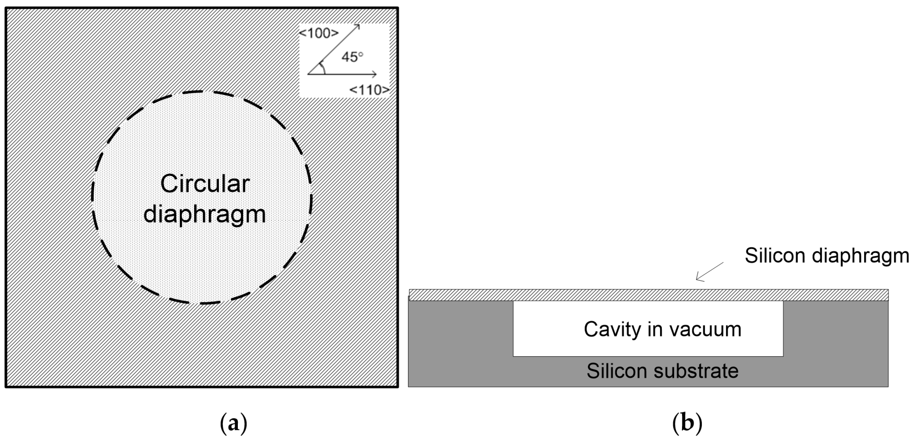
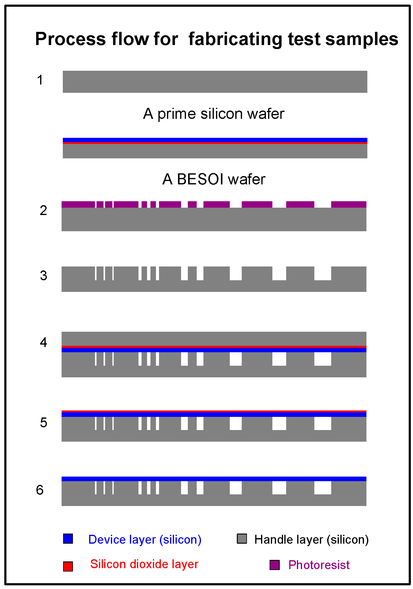
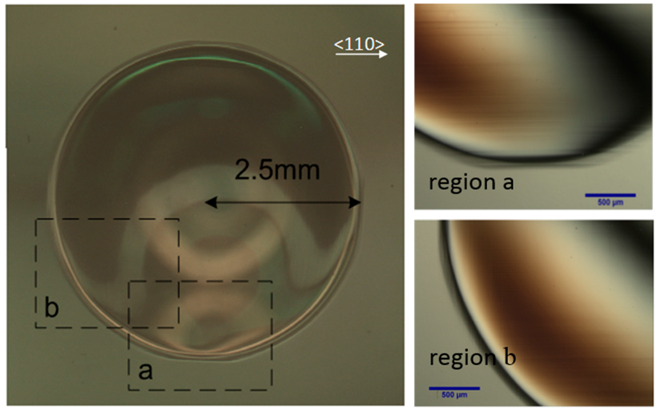
2.1. Microfabrication of SCS Diaphragms with Sealed Cavity


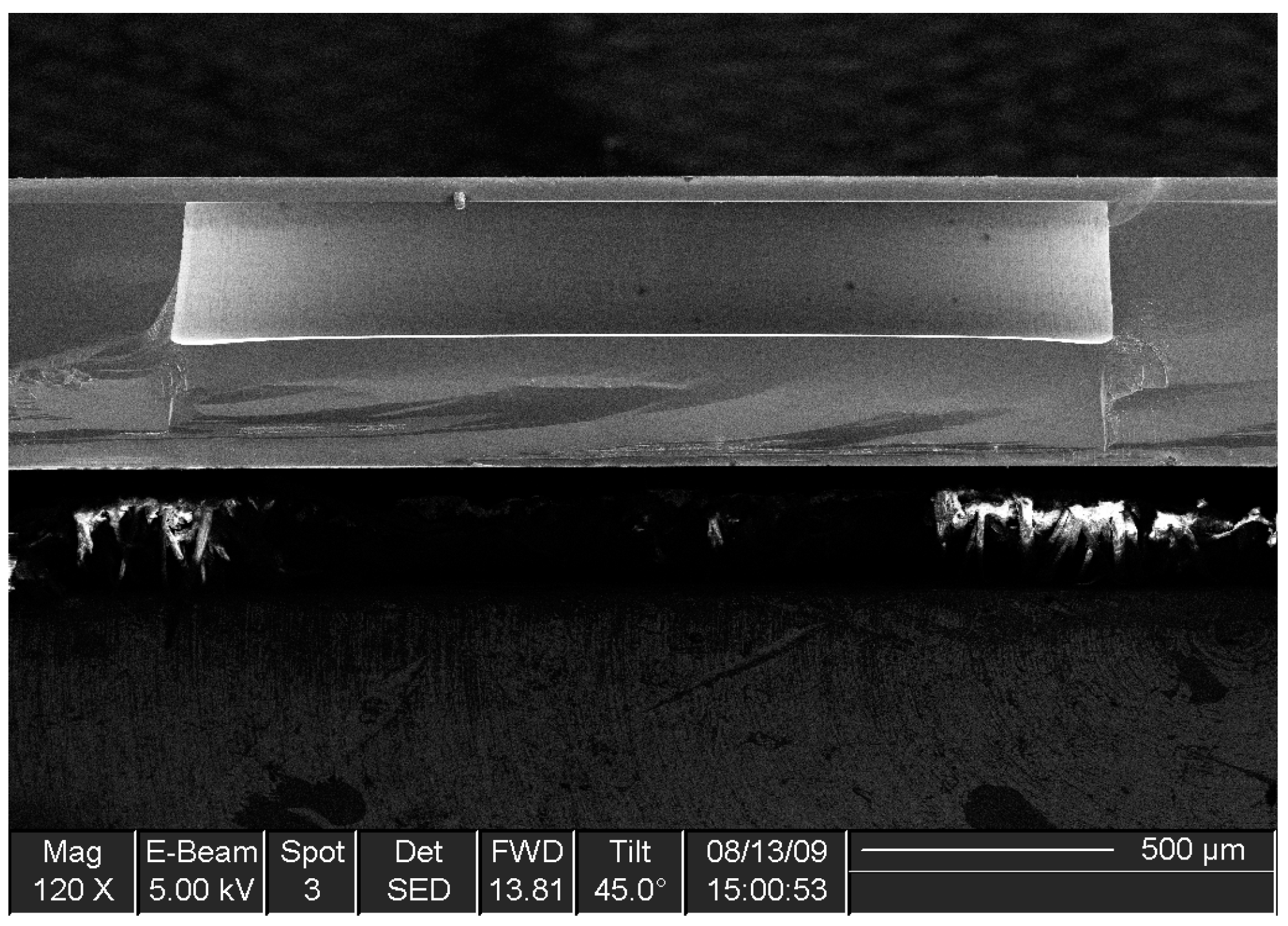
2.2. Thermal Treatment and Profile Measurement of SCS Diaphragms

| Anneal Temperature | Anneal Time (hour) | ||
|---|---|---|---|
| Stage A | Stage B | Stage C | |
| 600 °C | 1 | 68 | 68 |
| 800 °C | 1 | 15 | 15 |
| 900 °C | 1 | 10 | 10 |
3. Theoretical Prediction of Plastic Deformation
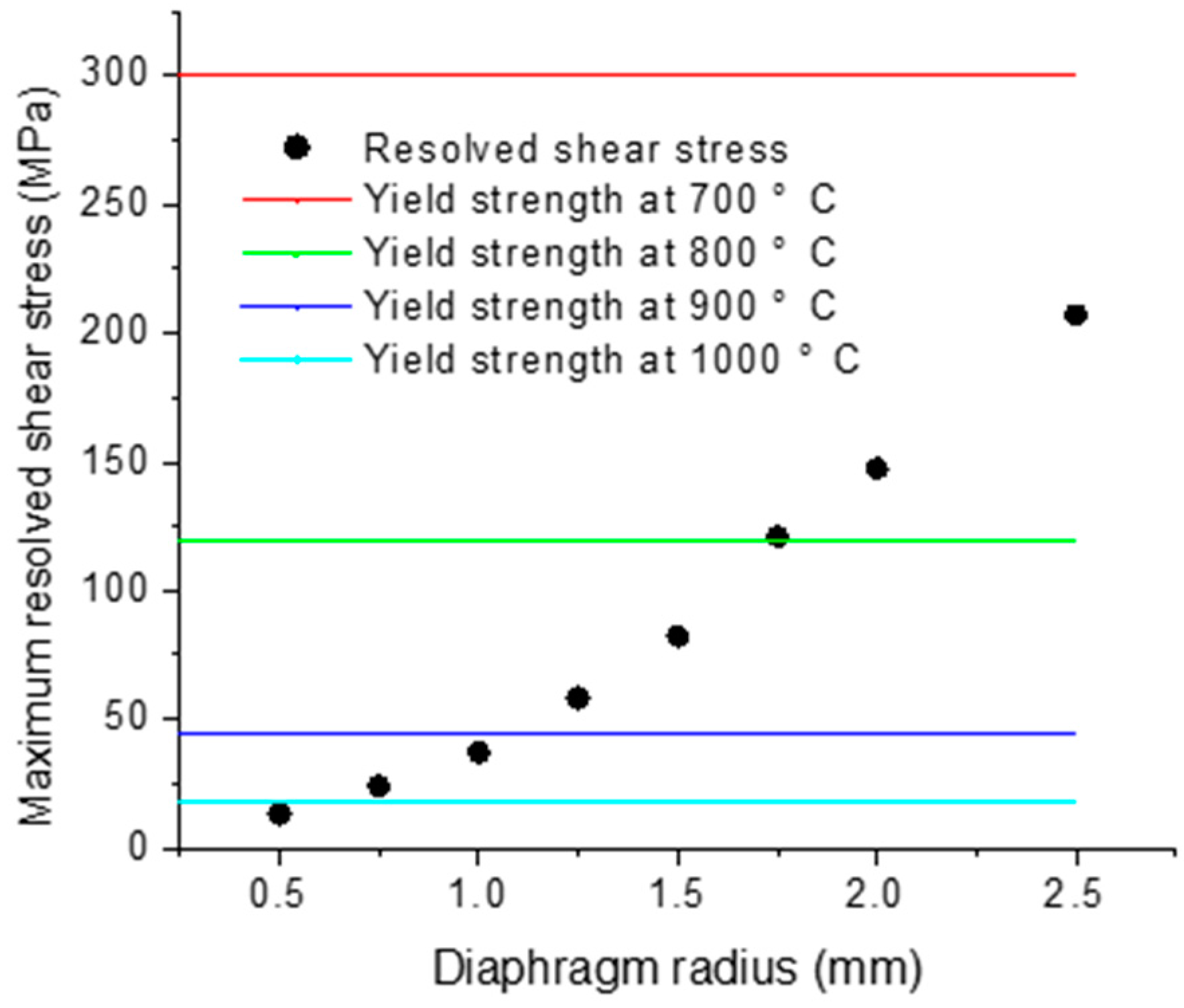
3.1. Resolved Shear Stress in SCS
| s | 1 | 2 | 3 | 4 | 5 | 6 | 7 | 8 | 9 | 10 | 11 | 12 |
|---|---|---|---|---|---|---|---|---|---|---|---|---|
| ns | 111 | 111 | 111 | |||||||||
| ls | 011 | 110 | 110 | 101 | 101 | 011 |
3.2. FEA Modeling
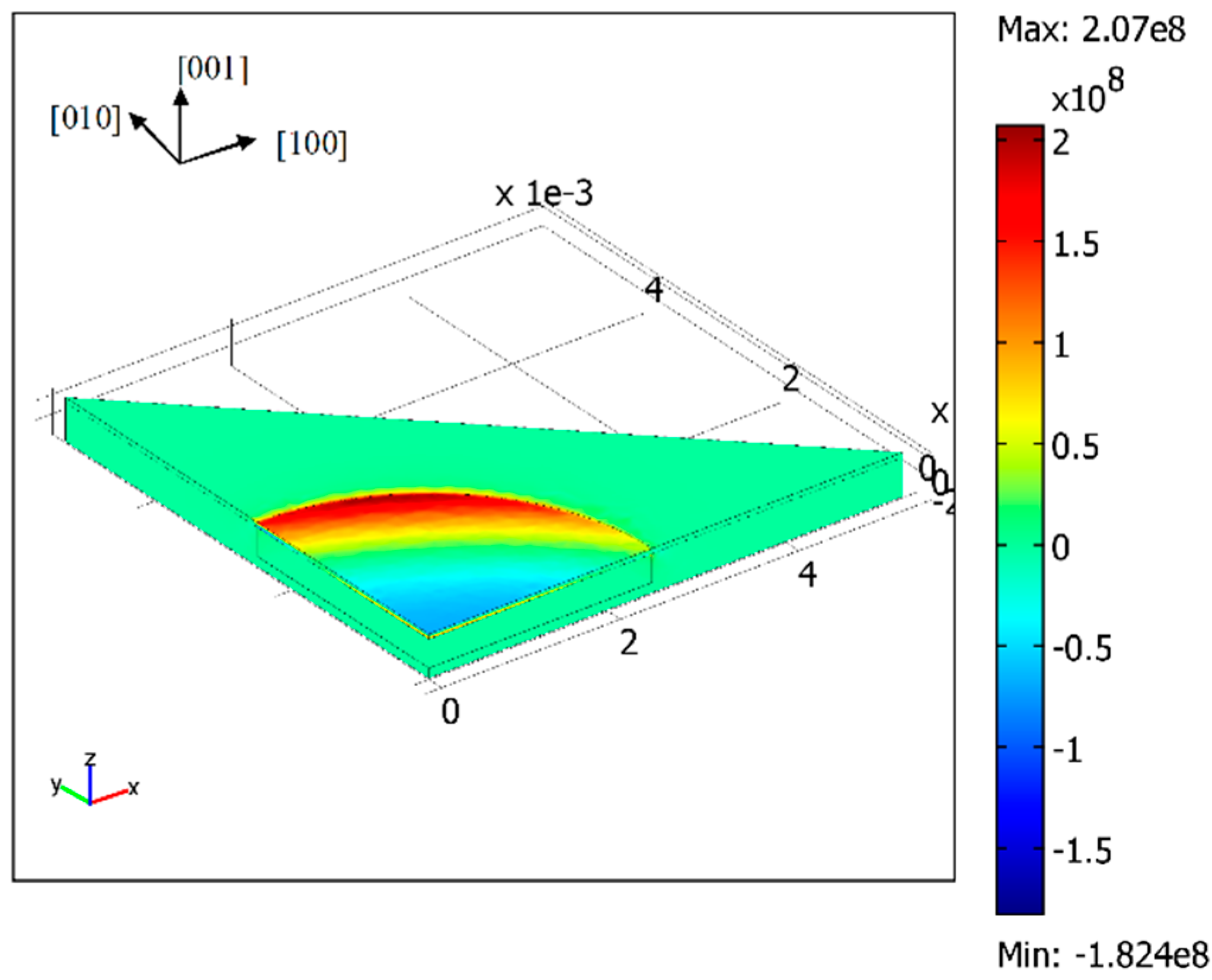
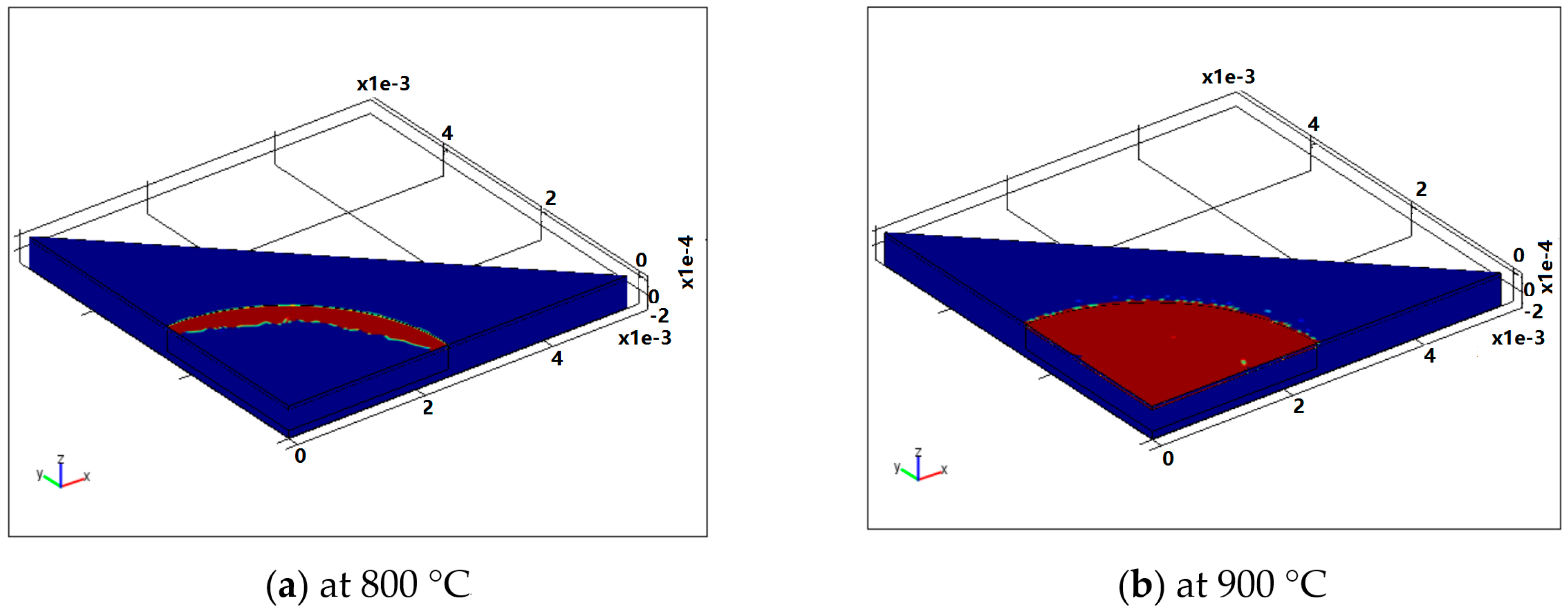
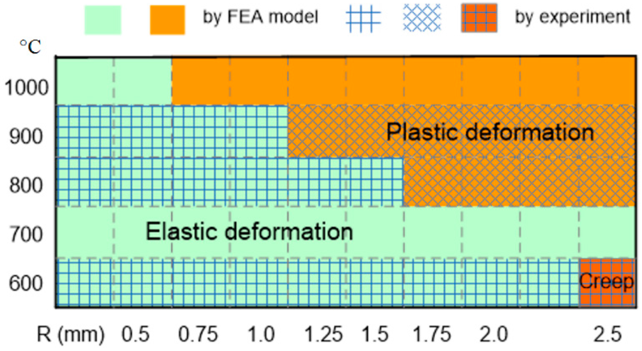
3.3. Occurrence of Plastic Deformation

3.4. The Plastic Zone

4. Experimental Results and Discussion
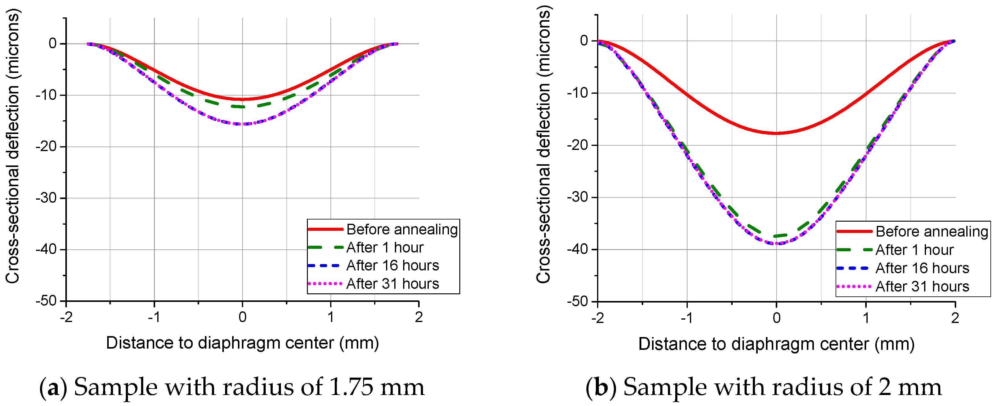
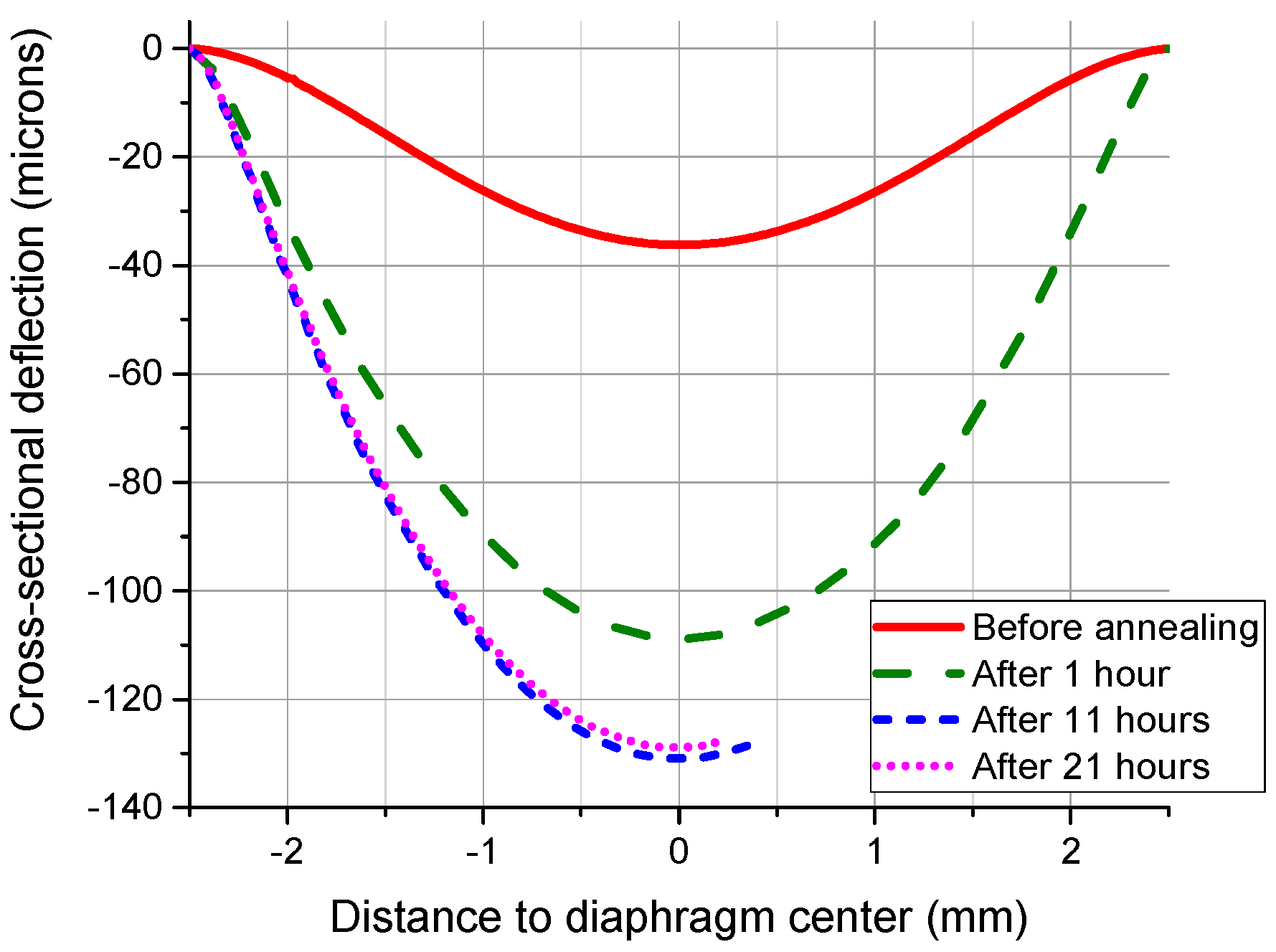
4.1. Plastic Deformation and Creep at High Temperature
| Total Annealing Time | 0.5 mm | 0.75 mm | 1 mm | 1.25 mm | 1.5 mm | 1.75 mm | 2 mm | 2.5 mm | |
|---|---|---|---|---|---|---|---|---|---|
| Before annealing | 0 h | 0.094 | 0.381 | 1.247 | 2.842 | 5.803 | 10.706 | 17.366 | 36.718 |
| After annealing A | 1 h | 0.097 | 0.398 | 1.226 | 2.841 | 5.804 | 10.756 | 17.542 | 37.457 |
| After annealing B | 69 h | 0.095 | 0.388 | 1.205 | 2.822 | 5.780 | 10.681 | 17.833 | 61.817 |
| After annealing C | 137 h | 0.090 | 0.390 | 1.208 | 2.811 | 5.775 | 10.621 | 17.990 | 74.780 |
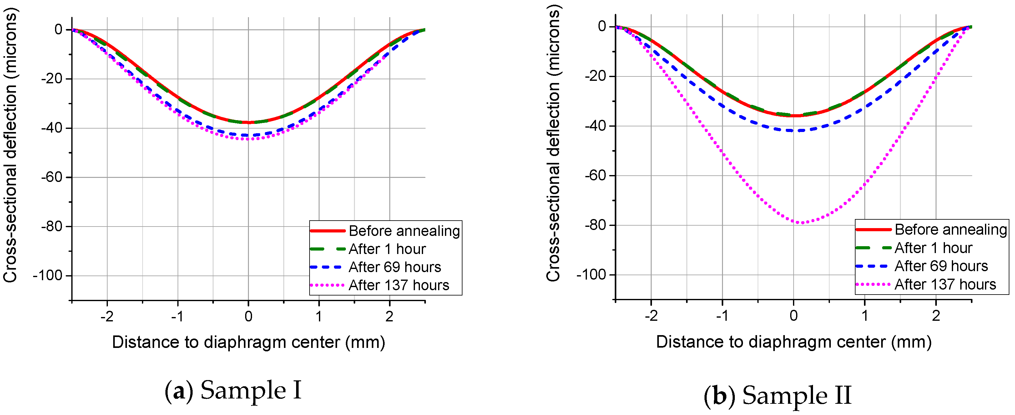
| Total Annealing Time | 0.5 mm | 0.75 mm | 1 mm | 1.25 mm | 1.5 mm | 1.75 mm | 2 mm | 2.5 mm | |
|---|---|---|---|---|---|---|---|---|---|
| Before annealing | 0 h | 0.087 | 0.375 | 1.149 | 2.895 | 5.902 | 10.790 | 17.517 | 37.090 |
| After annealing A | 1 h | 0.086 | 0.378 | 1.143 | 2.866 | 6.001 | 11.926 | 37.902 | 109.251 |
| After annealing B | 16 h | 0.084 | 0.383 | 1.156 | 2.877 | 6.027 | 13.491 | 38.518 | 110.096 |
| After annealing C | 31 h | 0.088 | 0.386 | 1.164 | 2.886 | 6.056 | 13.532 | 38.507 | 110.950 |

| Total Annealing Time | 0.5 mm | 0.75 mm | 1 mm | 1.25 mm | 1.5 mm | 1.75 mm | 2 mm | 2.5 mm | |
|---|---|---|---|---|---|---|---|---|---|
| Before annealing | 0 h | 0.091 | 0.394 | 1.164 | 2.884 | 5.887 | 10.755 | 17.308 | 37.211 |
| After annealing A | 1 h | 0.092 | 0.403 | 1.172 | 2.936 | 6.342 | 17.549 | 39.135 | 110.107 |
| After annealing B | 11 h | 0.089 | 0.400 | 1.176 | 3.192 | 10.665 | 35.278 | 86.778 | 134.680 |
| After annealing C | 21 h | 0.085 | 0.416 | 1.190 | 3.220 | 10.749 | 35.449 | 85.980 | 130.516 |


4.2. Discussion

5. Conclusions
Acknowledgments
Author Contributions
Conflicts of Interest
References
- Greenwood, J.C. Silicon in mechanical sensors. J. Phys. E: Sci. Instrum. 1988, 21, 1114–1128. [Google Scholar] [CrossRef]
- Yi, T.; Li, L.; Kim, C.-J. Microscale material testing of single crystalline silicon: Process effects on surface morphology and tensile strength. Sens. Actuators A Phys. 2000, 83, 172–178. [Google Scholar] [CrossRef]
- Hase, Y.; Bessho, M.; Ipposhi, T. SOI type pressure sensor for high temperature pressure measurement. SAE Int. 1994. [Google Scholar] [CrossRef]
- Mehregany, M.; Zorman, C.A.; Rajan, N.; Wu, C.H. Silicon carbide MEMS for harsh environments. P IEEE 1998, 86, 1594–1610. [Google Scholar] [CrossRef]
- Yasutake, K.; Murakami, J.; Umeno, M.; Kawabe, H. Jpn. J. Appl. Phys. 1982, 21, 288–290. [CrossRef]
- Mehra, A.; Ayon, A.A.; Waitz, I.A.; Schmidt, M.A. Microfabrication of high-temperature silicon devices using wafer bonding and deep reactive ion etching. J. Microelectromech. Syst. 1999, 8, 152–160. [Google Scholar] [CrossRef]
- Ned, A.A.; Okojie, R.S.; Kurtz, A.D. 6H-SiC pressure sensor operation at 600 °C. In Proceedings of the fourth International Conference of High Temperature Electronics, Albuquerque, NM, USA, 14–18 June 1998; pp. 257–260.
- Young, D.J.; Du, J.; Zorman, C.A.; Ko, W.H. High-temperature single-crystal 3C-SiC capacitive pressure sensor. Sens. J. 2004, 4, 464–470. [Google Scholar] [CrossRef]
- Wu, C.H.; Stefanescu, S.; Kuo, H.I.; Zorman, C.A.; Mehregany, M. Fabrication and testing of single crystalline 3C-SiC piezoresistive pressure sensors. In Proceedings of the 11th International Conference on Solid-State Sensors and Actuators, Munich, Germany, 10–14 June 2001.
- Quo, S.; Eriksen, H.; Childress, K.; Fink, A.; Hoffman, M. High temperature high accuracy piezoresistive pressure sensor based on smart-cut SOI. In Proceedings of IEEE 21st Conference on Micro Electro Mechanical Systems, Tucson, AZ, USA, 13–17 January 2008; pp. 892–895.
- Samuel, J.; Roberts, S.G. The Brittle-Ductile Transition in Silicon. I. Experiments. R. Soc. 1989, 421, 1–23. [Google Scholar] [CrossRef]
- Patel, J.R.; Chaudhuri, A.R. Macroscopic Plastic Properties of Dislocation-Free Germanium and Other Semiconductor Crystals. I. Yield Behavior. J. Appl. Phys. 1968, 34, 2788–2799. [Google Scholar] [CrossRef]
- Pearson, G.L.; Read, W.T.; Feldmann, W.L. Deformation and fracture of small silicon crystals. Acta Metall. Mater. 1957, 5, 181–191. [Google Scholar] [CrossRef]
- Sumino, K. Deformation behavior of silicon. Metall. Mater. Trans. A 1999, 30, 1465–1479. [Google Scholar] [CrossRef]
- Reppich, B.; Haasen, P.; Llschner, B. Kriechen von Silizium-Einkristallen. Acta Metall. Mater. 1964, 12, 1283–1288. [Google Scholar] [CrossRef]
- Myshlyaev, M.M.; Nikitenko, V.I.; Nesterenko, V.I. Dislocation Structure and Macroscopic Characteristics of Plastic Deformation at Creep of Silicon Crystals. Phys. Status Solidi B 1969, 36, 89–96. [Google Scholar] [CrossRef]
- Taylor, T.A.; Barrett, C.R. Creep and recovery of silicon single crystals. Mater. Sci. Eng. 1972, 10, 93–102. [Google Scholar] [CrossRef]
- Walters, D.S.; Spearing, S.M. On the flexural creep of single-crystal silicon. Scr. Mater. 2000, 42, 769–774. [Google Scholar] [CrossRef]
- Namazu, T.; Isono, Y.; Tanaka, T. Plastic deformation of nanometric single crystal silicon wire in AFM bending test at intermediate temperatures. J. Microelectromech. Syst. S 2002, 11, 125–135. [Google Scholar] [CrossRef]
- Frühauf, J.; Gärtner, E.; Jänsch, E. New aspects of the plastic deformation of silicon–prerequisites for the reshaping of silicon microelements. Appl. Phys. A 1999, 68, 673–679. [Google Scholar]
- Spearing, S.M. Materials issues in microelectromechanical systems (MEMS). Acta Mater. 2000, 48, 179–196. [Google Scholar] [CrossRef]
- Huff, M.A.; Nikolich, A.D.; Schmidt, M.A. Design of sealed cavity microstructures formed by silicon wafer bonding. J. Microelectromech. Syst. 1993, 2, 74–81. [Google Scholar] [CrossRef]
- Ren, J.; Ward, M.; Kinnell, P.; Gear, M.; Cradock, R. The experiment to study the behavior of microfabricated silicon diaphragms at 900 °C. In Proceedings of 35th International Conference on Micro & Nano Engineering (MNE09), Ghent, Belgium, 28 September–1 October 2009.
- Klaassen, E.H.; Petersen, K.; Noworolski, J.M.; Logan, J.; Maluf, N.I.; Brown, J. Silicon fusion bonding and deep reactive ion etching: a new technology for microstructures. Sens. Actuators A Phys. 1996, 52, 132–139. [Google Scholar] [CrossRef]
- Zhang, L.M.; Uttamchandani, D.; Culshaw, B.; Dobson, P. Measurement of Young's modulus and internal stress in silicon microresonators using a resonant frequency technique. Meas. Sci. Technol. 1990, 1, 1343–1346. [Google Scholar] [CrossRef]
- Cacho, F.; Orain, S.; Cailletaud, G.; Jaouen, H. A constitutive single crystal model for the silicon mechanical behavior: Applications to the stress induced by silicided lines and STI in MOS technologies. Microelectron. Reliab. 2007, 47, 161–167. [Google Scholar] [CrossRef]
- Mandel, J. Plasticité Classque et Viscoplasticité; Springer-Verlag: Berlin, Germany, 1971. [Google Scholar]
- Wortman, J.J.; Evans, R.A. Young’s Modulus, Shear Modulus, and Poisson’s Ratio in Silicon and Germanium. J. Appl. Phys. 1965, 36, 153–156. [Google Scholar] [CrossRef]
- Shmidt, V.A. Negative creep during bending of boron-doped silicon. Fizka Tverd. Tela 1972, 14, 3675–3676. [Google Scholar]
© 2016 by the authors; licensee MDPI, Basel, Switzerland. This article is an open access article distributed under the terms and conditions of the Creative Commons by Attribution (CC-BY) license (http://creativecommons.org/licenses/by/4.0/).
Share and Cite
Ren, J.; Ward, M.; Kinnell, P.; Craddock, R.; Wei, X. Plastic Deformation of Micromachined Silicon Diaphragms with a Sealed Cavity at High Temperatures. Sensors 2016, 16, 204. https://doi.org/10.3390/s16020204
Ren J, Ward M, Kinnell P, Craddock R, Wei X. Plastic Deformation of Micromachined Silicon Diaphragms with a Sealed Cavity at High Temperatures. Sensors. 2016; 16(2):204. https://doi.org/10.3390/s16020204
Chicago/Turabian StyleRen, Juan, Michael Ward, Peter Kinnell, Russell Craddock, and Xueyong Wei. 2016. "Plastic Deformation of Micromachined Silicon Diaphragms with a Sealed Cavity at High Temperatures" Sensors 16, no. 2: 204. https://doi.org/10.3390/s16020204
APA StyleRen, J., Ward, M., Kinnell, P., Craddock, R., & Wei, X. (2016). Plastic Deformation of Micromachined Silicon Diaphragms with a Sealed Cavity at High Temperatures. Sensors, 16(2), 204. https://doi.org/10.3390/s16020204