Synthesis of Nanocrystalline SnOx (x = 1–2) Thin Film Using a Chemical Bath Deposition Method with Improved Deposition Time, Temperature and pH

Abstract
: Nanocrystalline SnOx (x = 1–2) thin films were prepared on glass substrates by a simple chemical bath deposition method. Triethanolamine was used as complexing agent to decrease time and temperature of deposition and shift the pH of the solution to the noncorrosive region. The films were characterized for composition, surface morphology, structure and optical properties. X-ray diffraction analysis confirms that SnOx thin films consist of a polycrystalline structure with an average grain size of 36 nm. Atomic force microscopy studies show a uniform grain distribution without pinholes. The elemental composition was evaluated by energy dispersive X-ray spectroscopy. The average O/Sn atomic percentage ratio is 1.72. Band gap energy and optical transition were determined from optical absorbance data. The film was found to exhibit direct and indirect transitions in the visible spectrum with band gap values of about 3.9 and 3.7 eV, respectively. The optical transmittance in the visible region is 82%. The SnOx nanocrystals exhibit an ultraviolet emission band centered at 392 nm in the vicinity of the band edge, which is attributed to the well-known exciton transition in SnOx. Photosensitivity was detected in the positive region under illumination with white light.1. Introduction
Tin dioxide is an n-type wide-band gap semiconductor (Eg = 3.6 eV at 300 K) where inherent oxygen vacancies act as an n-type dopant [1,2]. Research on SnO2 attracts a lot of interest due to its many applications, such as in transparent electrodes, far-infrared detectors and high-efficiency solar cells [3,4]. It was recently reported that nanocrystalline SnO2 has different characteristics from bulk crystals. Nanocrystalline SnO2 thin films have also garnered attention since higher quality synthesis of SnO2 thin films was achieved.
A variety of methods, such as gas sensors [5], vacuum evaporation [6], chemical vapor deposition [7] and modified successive ionic layer adsorption and reaction [8] have been employed to prepare SnO2 thin films or nanoparticles. In the present investigation, nanocrystalline SnO2 thin films are prepared by using a simple chemical bath deposition (CBD) method. CBD, which is well known as a low temperature aqueous method for directly depositing large-area thin films of semiconductors has advantages over other techniques because it allows films to be deposited on substrates that might not be chemically or mechanically stable at high temperatures [9]. Moreover, CBD does not require sophisticated instruments such as vacuum systems. The starting chemicals are inexpensive and readily available and the parameters are easily controlled. Films deposited by this technique are now being developed for use in solar energy and other photonic applications, such as dye-synthesized solar cells [10], photothermal and photovoltaic conversions [11]. Decreasing the temperature and time for saving energy and a shift toward noncorrosive pH are the main objectives in chemical synthesis of TCO (transparent conductive oxide) for industry.
There are some literature reported the preparation of SnO2 films using chemical methods, and most of the films prepared by these methods need high temperatures or long deposition times and are prepared at corrosive pHs [12,13]. In this paper we prepared SnO2 films by a chemical bath deposition method in which a novel chelating reagent, triethanolamine, was used and deposition was conducted in a water bath to decrease the deposition time and temperature. Furthermore, the pH value was shifted to a noncorrosive region in this method. The optical, electrical and compositional characterization help to hasten the study of tin oxide potential application in transparent nanoelectrodes and transparent conductive oxide thin film solar cells.
2. Experimental Section
2.1. Preparation of SnOx Thin Films
The substrates used for the deposition of SnOx thin films were 76 × 25 mm2 sized glass slides. Prior to deposition, the glass slides were degreased with ethanol (0.1 M), etched with HCl solution (0.1 M) for 30 min and ultrasonically cleaned with deionized water for 50 min. Aqueous solution of 0.1 M tin chloride dihydrate, 0.5 M hydrogen peroxide, and complexing agents (0.15 M triethanolamine and 0.1 M ethylenediaminetetraacetic acid) were used to deposit SnOx thin films. Twenty mL of tin chloride dihydrate solution was mixed with 3.0 mL triethanolamine in a 100 mL beaker. A homogenous solution was obtained after stirring for several minutes. With continuous stirring, 5 mL ethylenediaminetetraacetic acid and 5 mL H2O2 were added. Deionized water was added to make the volume up to 50 mL. The pH values of the samples were adjusted to 2.0, 5.0 and 7.0, using ammonia and HCl solutions. Prior to deposition, substrates were heated to 120 °C and quickly mounted in the cold reaction solution. The reaction vessels were placed in a water bath at 30 °C for 30 min. The samples were removed from the water bath, and dried at room temperature.
2.2. Characterization Techniques
The composition and structure of the films were characterized by X-ray diffraction analysis using a Philips PM 1730 diffractometer from 20° to 80° with CuKα1 radiation (λ = 0.15405 nm). The surface morphology of the deposited films was studied using atomic force microscope (Quetint-250). The chemical composition of SnOx films was analyzed by an energy-dispersive X-ray analyzer (EDX) LEO 1455 VPSEM with Oxford Inca software. The optical transmission data in the wavelength range of 200–800 nm was recorded by a Lambda 2S Ultraviolet/Visible Spectrophotometer at room temperature. Thermogravimetric analysis of the powder of SnOx nanocrystalline was obtained by a TGA Perkin Elmer Thermal Analyzer. The samples were scanned at room temperature to 600 °C at a heating rate of 10 °C/min in the presence of nitrogen (50 mL/min). The photoluminescence properties were studied at room temperature using a Perkin Elmer LS-55 analyzer. The current-voltage characteristics in the dark as well as illumination (tungsten-halogen lamp with intensity of 100 W/Cm2), were measured by an ADCM 6243 DC voltage current source/monitor.
3. Results and Discussion
3.1. Composition Analysis
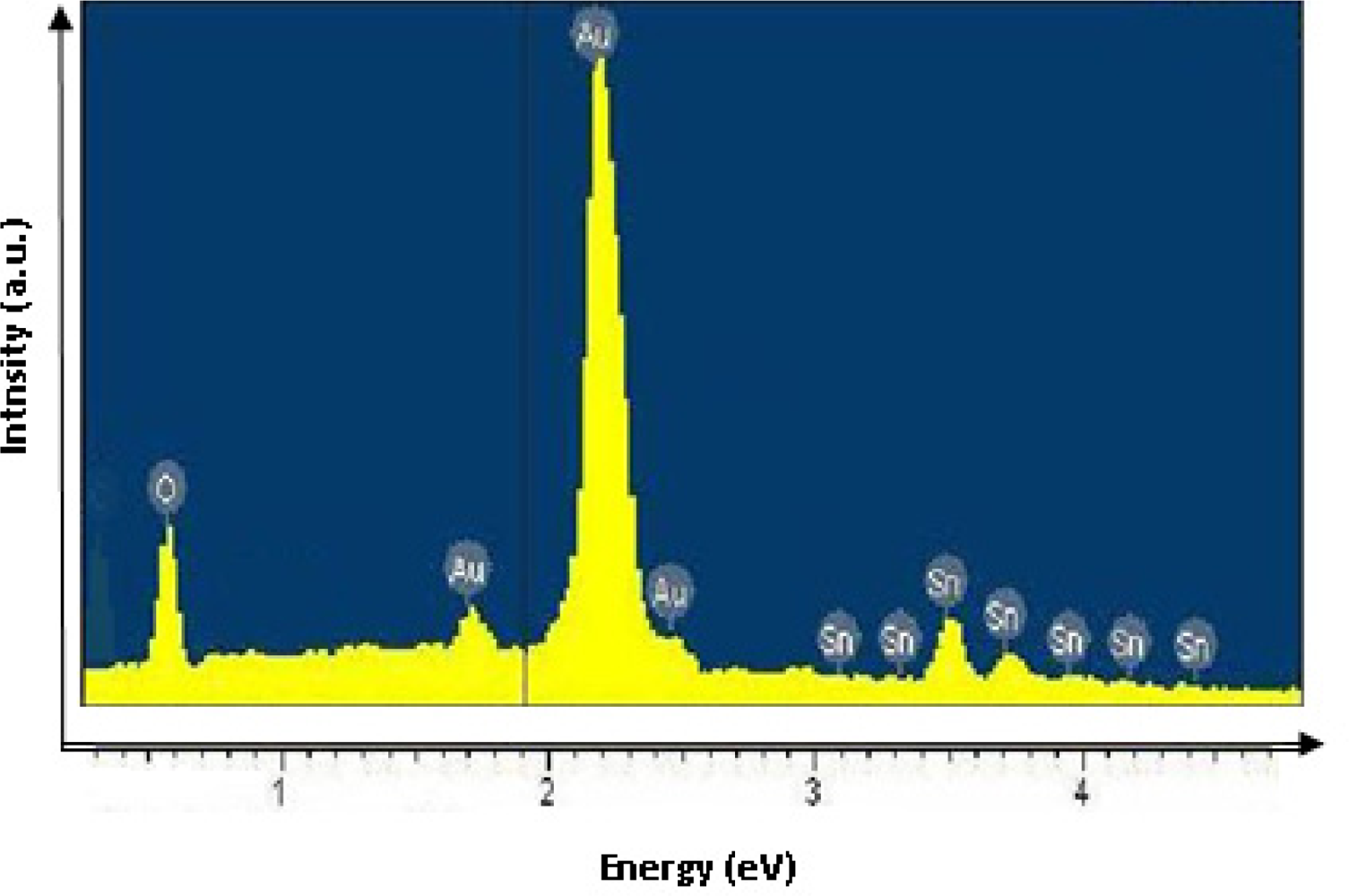
EDX was used to estimate the composition of the SnOx thin films. Figure 1 shows the EDX spectrum of SnOx thin film obtained by chemical bath deposition. The Au coating is reflected in the strong Au peak. The result illustrated in Figure 1 indicates the presence of oxygen and tin with a typical O/Sn ratio of 43/25 (or 1.72) which is close to the stoichiometry of the compound SnO2. SnO2 in its stoichiometric form acts as an insulator, but in its oxygen-deficient form tin dioxide behaves as an n-type semiconductor and the conductivity is thought to be due to intrinsic defect formation [14].
3.2. Structural Studies
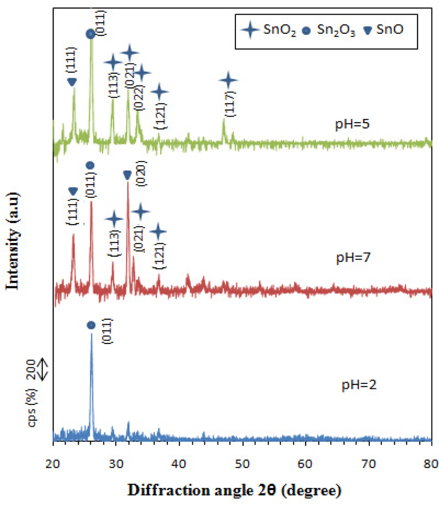
The XRD pattern of SnOx thin films (Figure 2) deposited by chemical bath deposition method for 30 min indicate that they are of a polycrystalline nature. From the XRD patterns several SnO2 peaks are detected for the samples prepared at pH 5.0 and 7.0. The observed d-values are in good agreement with the Joint Committee on Powder Diffraction Standard (JCPDS) data for the orthorhombic structure of SnO2 (reference code: 078-1063). The Miller indices are shown above the diffractions. For the sample deposited at pH of 5.0 the strongest peak is at 2θ of 31.8° (corresponding to (021) reflection). It indicates that the preferred orientation lies along (021) plane. The other smaller peaks were at 2θs of (29, 33.3, 36.6, and 47) corresponding to the (113), (022), (121) and (117) planes, respectively. The crystallite size on the film was calculated by using Scherrer's formula for the (021) peak for 2θ of 31.8° and was found to be 36 nm.
For the film deposited at pH of 7.0 some SnO peaks were also detected with high intensity, indicating the presence of side product and due to the non-optimum conditions used for the deposition of the SnO2 thin film. For the film deposited at pH of 2.0 no intense SnO2 peak was detected.
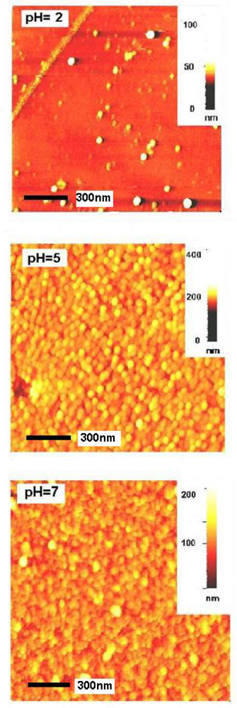
3.3. Surface Morphology
Film morphology was examined using atomic force microscopy (AFM). Figure 3 illustrates the two-dimensional images of the films deposited at various pH levels. Figure 3 reveals incomplete growth of the films deposited at pH of 2.0 and uniform growth at pH of 5.0 or 7.0.
The formation of spherical, compact and nano sized grains on an amorphous background on films deposited at pH of 5.0 is an indication of nucleation by multiple growths. No pinholes or cracks were seen in the sample. The thickness of the film was 230 nm. The surface roughness of the film was about 8.74 nm, which is due to nucleation of grains by multiple growths that increases the incident light trapping effect of transparent tin oxide thin film for solar cell applications.
3.4. Optical Properties
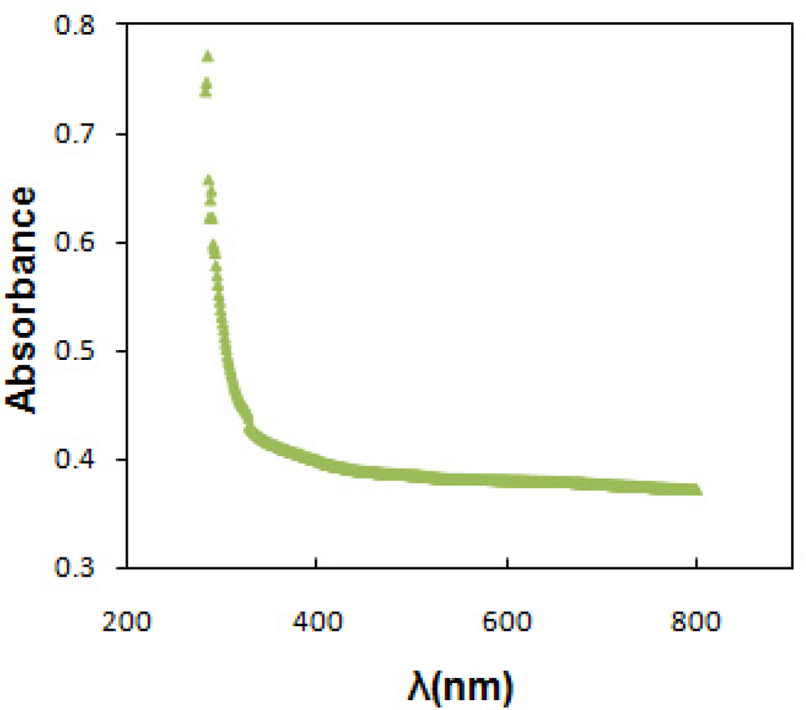
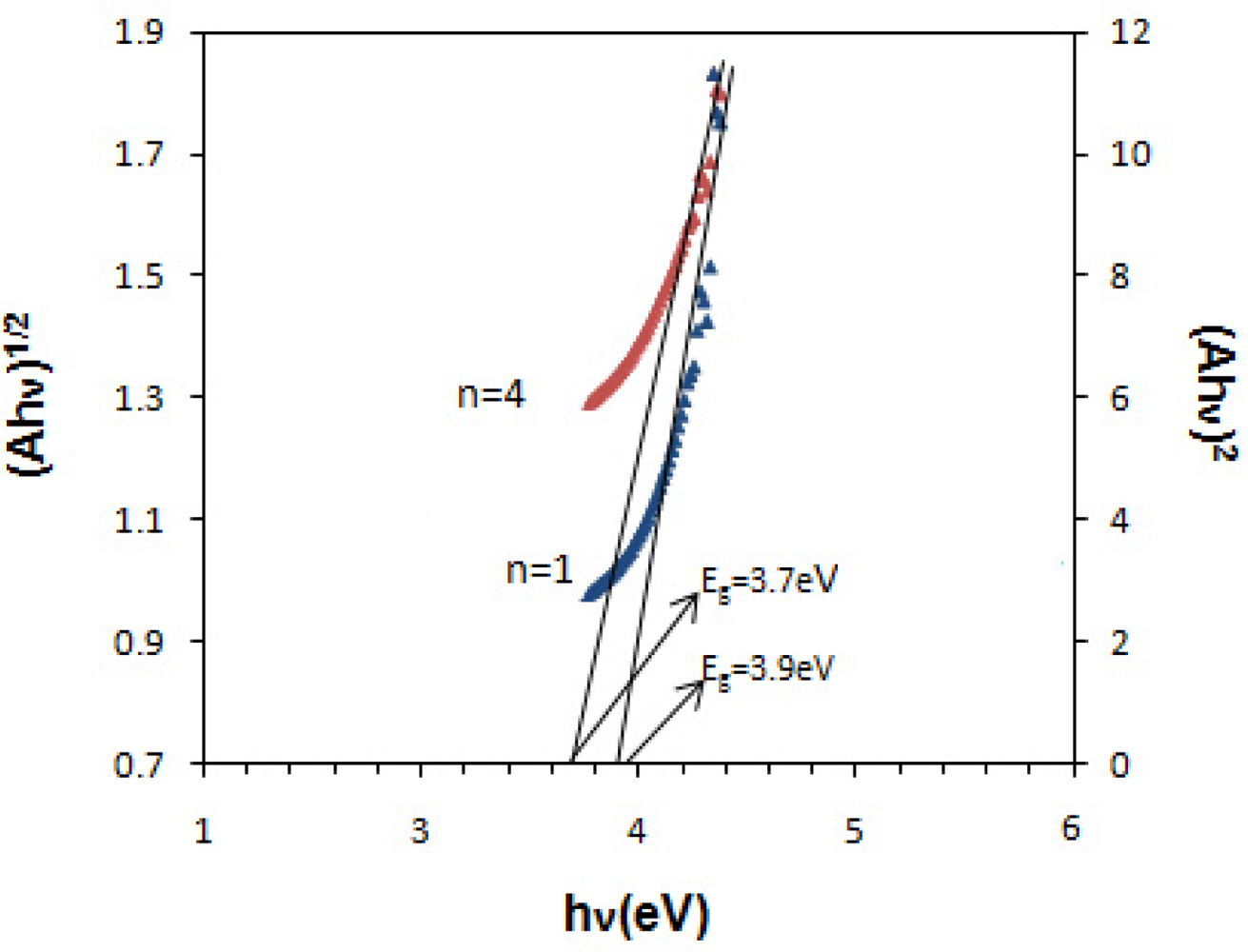
Optical absorption was utilized to estimate band gap and type of optical transition. Figure 4 shows the absorption spectrum versus wavelength of SnOx thin film deposited on glass substrate at pH of 5.0 and temperature of 30 °C. The optical data was then analyzed using the Stern equation for near-edge absorption:
The band gap value were determined from the intercept of the straight line portion in maximum absorbance of the (Ahν)2/n against the hν on the hν axis. In this case, the band gap of 3.9 eV and 3.7 eV was estimated for direct and indirect transition between valence and conduction bands of SnOx thin film. The wide band gap and minimum absorbance of deposited SnOx thin film in the UV-Visible range indicates the potential application of prepared thin films as window layer in solar cell device [3]. Table 1 shows the structural and optical characteristics of deposited SnOx nanocrystalline thin film on glass substrate.
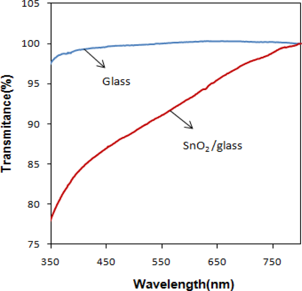
High transmittance at visible-light wavelengths is a key factor for the semiconducting material in a transparent device, such as the SnO2 thin film solar cell or transistor. Figure 6 compares the transmittance of the SnOx/glass thin film and glass slides. The glass used has 96% optical transmittance in the visible part of the spectrum. The average transmittance for SnOx/glass in the visible part of the spectrum is comparable with glass and is more than 82%. This indicates that the deposited SnOx thin film can be used as a transparent conductive oxide layer in solar cell devices.
3.5. Photoluminescence
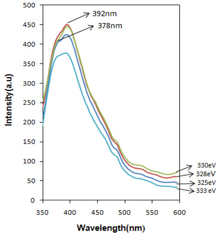
Photoluminescence (PL) spectra of the SnOx nanocrystalline were obtained in the wavelength range from 350 to 600 nm. The room temperature optical luminescence (Figure 7) from SnOx nanocrystalline excited with various photon energies exhibit a strong emission band at 392 nm (3.17 eV) and a shoulder in 378 nm (3.28 eV). The expected near band edge was detected around 345 nm for direct transition and 335 nm for indirect transition, which is originated from exciton recombination of electron in the Sn ‘4d’ conduction band with a hole in the O ‘2p’ valence band. The observed shift to the visible range can be attributed to the recombination of photo-generated holes with singly ionized charge states in intrinsic defects such as oxygen vacancies, Sn interstitials, or impurities [15–17].
3.6. Photosensitivity
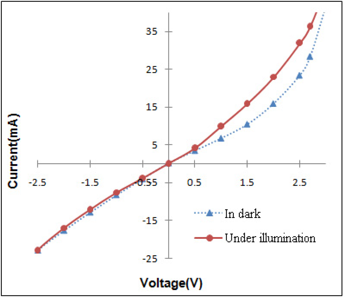
As thin oxide films are expected to be semiconductors they should be sensitive to the light, with energy higher than their Eg and show a photocurrent in the region corresponding to its minority carrier current flow. Figure 8 shows the photosensitivity of the SnOx thin film in the dark and under illumination. The lower value corresponds to the dark current, while the upper value of the current corresponds to the photocurrent when the sample, employed as anode, was illuminated. The fact that the photocurrent occurs on the positive potentials region indicates that electrons are minority carriers of the film and their concentration was then enhanced by illumination. Thus, the films prepared are n-type semiconductor and can be deployed as photoanode in the PECs (photoelectrochemical cells) application to facilitate oxidation on the electroactive species in the solution.
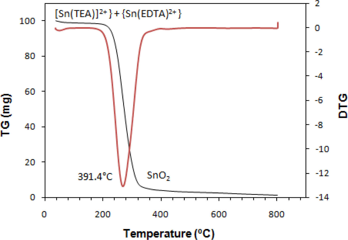
3.7. Thermogravimetric Analysis
TG-DTG (thermogravimetry-derivative thermogravimetry) analysis was conducted to characterize the effects of heat treatment on the powder obtained from drying of precursor solution for nanocrystalline SnOx. However the characteristics of powder and film were not exactly the same, the heat treatment temperature can be obtained from the TG-DTG analysis. Figure 9 is the results of thermogravimetric measurements for prepared SnOx nanocrystalline.
The weight loss for nanocrystalline SnOx occured at a temperature between 184 °C to 269.2 °C, which is related to the decomposition of TEA from the [Sn(TEA)]2+complex and evaporation of solvent. It shows a residue retention of 3.9% at T > 320 °C. It can be concluded that to complete the crystallization of SnO2 and evaporation of complexing agent and water, the heat treatment should be conducted over 269.2 °C.
4. Conclusions
A simple chemical bath deposition technique was successfully utilized to synthesize nanocrystalline SnOx thin films with decreased time of deposition and bath temperature and increased pH to the noncorrosive region by using TEA as a complexing agent. The preferred orientation lies along the (021) plane. AFM analysis showed a compact texture with small uniform grains of about 36 nm and 230 nm thick for the film deposited at pH of 5.0. EDX revealed that the average O/Sn atomic percentage is 1.72. Optical data analysis illustrated a direct band gap at 3.9 eV and an indirect transition at 3.7 eV. The wide band gap (3.9) and high transmittance (>82%) makes it possible for these thin films to be used in solar cell devices as transparent conductive oxide layers. The photoluminescence spectra of the nanocrystalline SnOx exhibited a strong UV exciton peak at room temperature. The temperature for heat treatment of the as deposited thin film was found to be above 391 °C using TGA analysis.
References
- Lee, SW; Kim, YW; Chen, H. Electrical properties of Ta-doped SnO2 thin films prepared by chemical-vapor deposition method. Appl. Phys. Lett 2001, 78, 350–352. [Google Scholar]
- Mason, MG; Hung, LS; Tang, CW; Lee, ST; Wong, KW; Wang, M. Characterization of treated indium-tin-oxide surfaces used in electroluminescent devices. J. Appl. Phys 1999, 86, 1688–1692. [Google Scholar]
- Peaker, AR; Horsley, B. Transparent conducting films of Antimony doped tin oxide on glass. Rev. Sci. Instrum 1971, 42, 1825–1827. [Google Scholar]
- Watson, J. The tin oxide gas sensor and its application. Sens. Actuat 1984, 5, 29–42. [Google Scholar]
- Barsan, N; Weimar, U. Understanding the fundamental principles of metal oxide based gas sensors; the example of CO sensing with SnO2 sensors in the presence of humidity. J. Phys. Condens. Matter 2003, 15, R813–R839. [Google Scholar]
- Nuli, YN; Zhao, SL; Qin, QZ. Nanorystalline tin oxides and nickel oxide film anodes for Li-ion batteries. J. Power Sources 2003, 114, 113–120. [Google Scholar]
- Duverneuil, P; Maury, F; Pebere, N; Senocq, F; Vergnes, H. Chemical vapor deposition of SnO2 coatings on Ti plates for the preparation of electrocatalytic anodes. J Surf Coat Technol 2002, 151–152, 9–13. [Google Scholar]
- Deshpande, NG; Vyas, JC; Sharma, R. Preparation and characterization of nanocrystalline tin oxide thin films deposited at room temperature. J. Thin Solid Films 2008, 516, 8587–8593. [Google Scholar]
- Hodes, G; Dekker, M. Chemical Solution Deposition of Semiconductor Films; CRC Press: Boca Raton, FL, USA, 2002. [Google Scholar]
- Mane, RS; Lee, WJ; Lokhande, CD; Cho, BW; Han, S-H. Controlled repeated chemical growth of SnO films for dye-sensitized solar cells. Curr. Appl. Phys 2008, 8, 549–553. [Google Scholar]
- Salem, AM; Abou-Helal, MO. Chemical bath deposition of tin selenide thin films. Mater. Chem. Phys 2003, 9849, 1–6. [Google Scholar]
- Igbinovia, EO; Ilenikhena, PA. Improved chemical deposition and thermal emittance of tin (iv) oxide (SnO2) thin films for photothermal conversion of solar energy and possible applications. Int. J. Phys. Sci 2010, 5, 1770–1775. [Google Scholar]
- Masuda, Y; Ohji, T; Kato, K. Room-temperature synthesis of tin oxide nano-electrodes in aqueous solutions. Thin Solid Films 2009, 518, 850–852. [Google Scholar]
- Godinho, KG; Walsh, A; Watson, GW. Energetic and electronic structure analysis of intrinsic defects in SnO2. J. Phys. Chem. C 2008, 113, 439–448. [Google Scholar]
- Özgur, Ü; Alivov, YI; Liu, C; Teke, A; Reshchikov, MA; Doğan, S; Avrutin, V; Cho, S-J; Morkoç, H. A comprehensive review of ZnO materials and devices. J Appl Phys 2005. [Google Scholar] [CrossRef]
- Kim, T-W; Kazawoe, T; Yamazaki, S; Ohtsu, M; Sekiguchi, T. Low-temperature orientation-selective growth and ultraviolet emission of single-crystal ZnO nanowires. J. Appl. Phys. Lett 2004, 84, 3358–3360. [Google Scholar]
- Qiu, Z; Wong, KS; Wu, M. Microcavity lasing behavior of oriented hexagonal ZnO nanowhiskers grown by hydrothermal. J. Appl. Phys. Lett 2004, 84, 2739–2741. [Google Scholar]


| pH | Crystalline structure | t (nm) | Ra (nm) | Eg(eV) | Size (nm) | T (%) | PL | ||
|---|---|---|---|---|---|---|---|---|---|
| Direct transition | Indirect transition | Intensity % | Position (nm) | ||||||
| =5 | orthorhombic | 230 | 8.74 | 3.9 | 3.7 | 36 | >85 | 445 | 392 |
| =7 | orthorhombic | 180 | 17.1 | 4 | 3.8 | 52 | >76 | 410 | 390 |
| =2 | orthorhombic | 20 | 1.46 | 3.9 | 3.7 | 500 | >98 | 320 | 392 |
Note: t = thickness, T = transmittance, Ra = surface roughness.
© 2011 by the authors; licensee MDPI, Basel, Switzerland. This article is an open access article distributed under the terms and conditions of the Creative Commons Attribution license (http://creativecommons.org/licenses/by/3.0/).
Share and Cite
Ebrahimiasl, S.; Yunus, W.M.Z.W.; Kassim, A.; Zainal, Z. Synthesis of Nanocrystalline SnOx (x = 1–2) Thin Film Using a Chemical Bath Deposition Method with Improved Deposition Time, Temperature and pH. Sensors 2011, 11, 9207-9216. https://doi.org/10.3390/s111009207
Ebrahimiasl S, Yunus WMZW, Kassim A, Zainal Z. Synthesis of Nanocrystalline SnOx (x = 1–2) Thin Film Using a Chemical Bath Deposition Method with Improved Deposition Time, Temperature and pH. Sensors. 2011; 11(10):9207-9216. https://doi.org/10.3390/s111009207
Chicago/Turabian StyleEbrahimiasl, Saeideh, Wan Md. Zin Wan Yunus, Anuar Kassim, and Zulkarnain Zainal. 2011. "Synthesis of Nanocrystalline SnOx (x = 1–2) Thin Film Using a Chemical Bath Deposition Method with Improved Deposition Time, Temperature and pH" Sensors 11, no. 10: 9207-9216. https://doi.org/10.3390/s111009207