Article

Semiconductor Three-Dimensional Photonic Crystals with Novel Layer-by-Layer Structures

1
Institute of Industrial Science, the University of Tokyo, Tokyo 153-8505, Japan
2
Institute for Nano Quantum Infromation Electronics, the Univesrity of Tokyo, Tokyo 153-8505, Japan
*
Author to whom correspondence should be addressed.
Photonics 2016, 3(2), 34; https://doi.org/10.3390/photonics3020034
Submission received: 5 April 2016 / Revised: 16 May 2016 / Accepted: 17 May 2016 / Published: 20 May 2016
(This article belongs to the Special Issue 3D- and 2D-Nanofabrication for Photonic Devices)

Abstract

:
Three-dimensional photonic crystals (3D PhCs) are a fascinating platform for manipulating photons and controlling their interactions with matter. One widely investigated structure is the layer-by-layer woodpile structure, which possesses a complete photonic bandgap. On the other hand, other types of 3D PhC structures also offer various possibilities for controlling light by utilizing the three dimensional nature of structures. In this article, we discuss our recent research into novel types of layer-by-layer structures, including the experimental demonstration of a 3D PhC nanocavity formed in a <110>-layered diamond structure and the realization of artificial optical activity in rotationally stacked woodpile structures.

1. Introduction

Engineering the electromagnetic environment is a powerful tool not only for controlling light propagation and localization but also for tailoring various light matter interactions such as light emission. Photonic crystals (PhCs) [1] are an important platform that enables the realization of artificial electromagnetic environments. Two-dimensional (2D) PhC slabs are now well developed, and ultrahigh cavity quality factor, Q, of ~9 million has been achieved [2]. Taking advantage of the high Q factors and small mode volumes of 2D PhC nanocavities, low threshold nanocavity lasers [3,4,5,6,7,8,9] have also been demonstrated. High-Q 2D PhC nanocavities also allow the exploration of the fundamental physics of quantum-dot (QD)-based cavity quantum electrodynamics (CQED) and other related phenomena [9,10,11,12,13,14].
Expanding this technology into the third dimension (i.e., fabricating three-dimensional (3D) PhCs) can provide much broader opportunities to manipulate photons and their interactions with materials. For example, a complete photonic bandgap (cPBG), which prohibits light propagation along any direction in any polarization state, offers the ultimate ability to manipulate light-matter interactions [15]. Moreover, utilizing the third dimension will add new degrees of freedom for controlling the optical response of structures. For instance, twisting a structure about an axis introduces a structural chirality, which leads to the emergence of optical activity within the structure even though it is composed of achiral materials.
Since the demonstration of “Yablonovite,” a type of 3D PhC possessing a cPBG, at microwave wavelengths [16], 3D PhCs operating at optical wavelengths, have been receiving great interest. However, difficulties in fabrication were a big obstacle for diving into the “3D PhC world”. Recently, various fabrication technologies for 3D PhCs at optical wavelengths, including self-assembly methods [17,18], top-down approaches such as a combination of photoelectrochemical etching and focused-ion-beam drilling [19] and one-step two-directional deep etching [20,21], bottom-up methods like laser direct writing [22], layer-by-layer methods including wafer fusion [23,24] and micro-manipulation [25,26], and hybrid approaches [27,28] have been developed (see also [29]). In particular, layer-by-layer methods, where separately prepared layers are stacked to create a PhC, have been adopted to demonstrate optical components including waveguides [30] and cavities [26,31,32] at near-infrared wavelengths around 1.2~1.6 μm. Three-dimensional guiding of light [33] is one of the originally expected functions of 3D PhCs. A 3D PhC nanocavity with Q as high as ~38,500 has also been reported [34]. Moreover, surface modes in 3D PhCs [35,36] have been investigated as a new frontier of 3D PhC science.
One particular advantage of layer-by-layer methods is the ability to construct 3D PhCs by combining several different materials and/or layers. Consequently, we can introduce active materials like semiconductor quantum wells and QDs selectively into passive 3D PhCs. Lasing oscillation in GaAs-based 3D PhC nanocavities with InAs QD gain has been demonstrated [34]. Furthermore, thanks to the material flexibility of this fabrication method, a hybrid-type 3D PhC nanocavity laser has also been reported [37], in which a GaAs nanocavity with InAs QDs was embedded in a Si-based passive 3D PhC. Moreover, CQED effects in 3D PhCs have also been demonstrated, such as the acceleration and suppression of radiative decay of single QDs embedded in a 3D PhC nanocavity [9,38]. In these studies, the so-called “woodpile” structure [39] was used as the base structure. However, there are many other types of 3D PhC structure that can be fabricated using layer-by-layer methods. Non-woodpile structures will be able to provide new approaches for controlling photons and to expand the possibility and functionality of 3D PhCs.
In this article, we will review our recent studies on 3D PhCs with non-woodpile layer-by-layer structures. In Section 2, we will discuss nanocavities formed in 3D PhCs with a <110>-layered diamond structure. Compared with the widely used woodpile structure, the <110>-layered diamond structure can improve the cavity Q of a nanocavity embedded in a 3D PhC with a limited in-plane size. After discussing numerical analysis, the experimental realization of nanocavities in <110>-layered diamond PhCs will be described. Artificial optical activity in semiconductor chiral 3D PhCs will be discussed in Section 3. The chiral 3D PhCs consist of semiconductor-air gratings stacked with different angles. Broadband circular dichroism and giant optical rotation are observed in semiconductor chiral 3D PhCs.

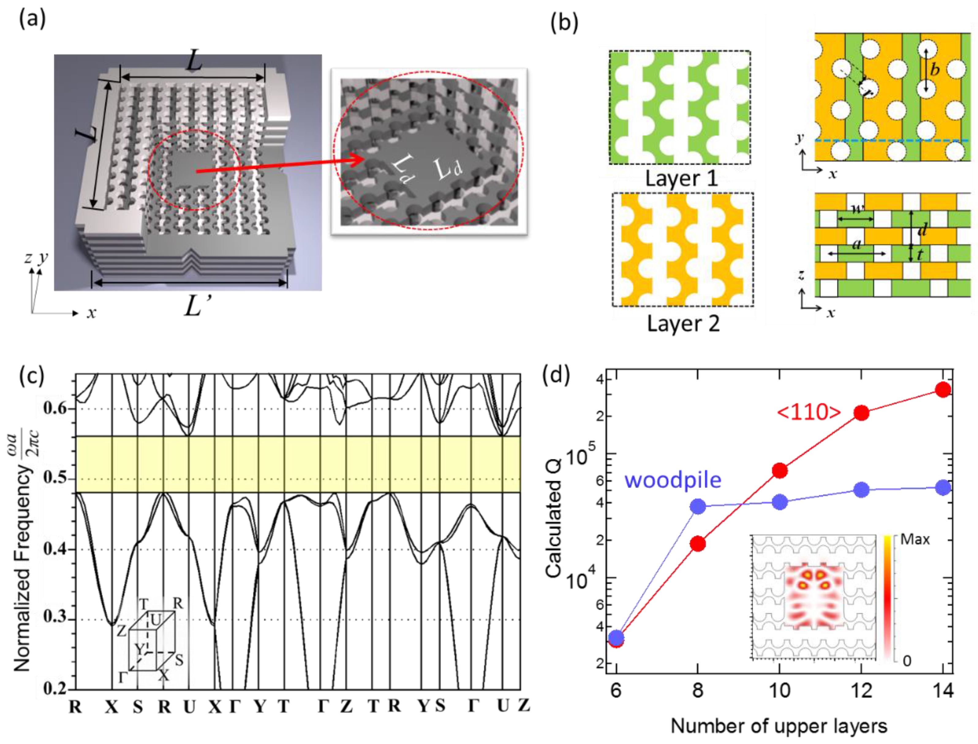
2. Nanocavity Formed in <110>-Layered Diamond 3D PhCs

High-Q 3D PhC nanocavitis will play key roles not only as one of fundamental optical elements for constructing 3D optical circuits but also as a platform for studying CQED effects in ultimately controlled electromagnetic environments. 3D PhC nanocavity lasers have already been reported [34,37]. However, the highest cavity Q reported so far is still only ~38,500 [34], which is much lower than that achievable with 2D PhC counterparts [2]. The recorded Q is limited by a finite in-plane size of the structure. One of the simplest approaches to increase the cavity Q is to enlarge the in-plane size of the structure. However, this is practically difficult when using the micromanipulation technique, which was used for the demonstration. Another approach is to use a different structure that sustains a higher Q under the condition of a limited in-plane size. Besides the practical importance of such a novel structure, realizing high-Q 3D PhC nanocavities within smaller in-plane area is also beneficial for densely integrating optical elements in 3D PhCs. As one possible new structure, we examined a <110>-layered diamond structure [40,41,42,43] as the base PhC structure. The widely investigated woodpile structure is also based on diamond lattice. The diamond symmetry enables to open a wide cPBG as discussed in [43,44].

2.1. <110>-Layered Diamond Structure and Numerical Analysis

Figure 1a shows a schematic illustration of a <110>-layered diamond structure embedding a nanocavity with square shape (Ld × Ld). The <110>-layered diamond structure consists of alternately stacked plates with two different in-plane patterns, which are shown in Figure 1b (left) as “Layer 1” and “Layer 2.” The plates are stacked along a <110> direction of the original diamond lattice. The top and side views of stacked structure are also shown in Figure 1b (right top and right bottom, respectively). As shown in the top view, a face-centered rectangular array of circular holes along the stacked direction is introduced, which modulates the rod width in each layer. On the other hand, as shown in the side view, rods in layers also form a face-centered rectangular lattice. The structure can be recognized as an inverted woodpile structure [40] with circular and square pores along the [110] and [1,2,3,4,5,6,7,8,9,10] directions, respectively. The parameters defining the structure are shown in Figure 1b. The photonic band diagram of the <110>-layered diamond structure is shown in Figure 1c. Here, we used the following parameter values: a = 630 nm, r = 156 nm, b = 445 nm, d = 450 nm, t = 225 nm, and w = 392 nm. The refractive index of plates was set as 3.4. A relatively large cPBG with the normalized cPBG width of ~15.3% is formed around the normalized frequency of ~0.52. The cPBG covers the wavelength range from 1123 nm to 1310 nm for the parameters used here. As discussed in the next subsection, we utilized light emission from self-assembled InAs QDs for experimentally characterizing nanocavities. Thus, the cPBG range was designed so that the center of cPBG is roughly matched to the wavelength of QD ground state emission (1200 nm in the present case). The cPBG range can be tuned to a spectral region suitable for a particular application, for instance to 1.55-μm telecommunication wavelength region, by changing the structural parameters of the PhC. More detail descriptions of the <110>-layered diamond structure and analysis on the effect of structural parameters on the cPBG width are found in our previous report [45].
This type of <110>-layered diamond structure has been discussed in [43] very briefly but nanocavities in the structure have not been investigated. We calculated cavity mode frequencies and corresponding Qs for a square shaped cavity with Ld = 1.45 μm (see Figure 1a). In the calculations, L = 5 μm and L’ = 10 μm, which were the size of the PhC pattern and the plate size used in a previous work [34]. Other parameters are the same as those for Figure 1c. Here, we focus our discussions on a cavity mode located around the center of the cPBG. The cavity mode wavelength is 1198 nm. The in-plane electric field energy distribution at the center of the middle cavity plate is shown in the inset of Figure 1d. Due to the relatively large size of cavity, many cavity modes exist within the cPBG. We found 18 modes below the frequency of the mode. Figure 1d shows the value of Q for the mode as a function of the number of plates above the plate containing the cavity structure. Here, we use 14 plates below the cavity plate. In the same graph, the Qs of a square-shaped nanocavity formed in a woodpile structure, which has a face-centered-cubic lattice with the same lattice constant of 630 nm and the optimum rod width of 189 nm for maximizing the cPBG width [44], are also plotted. Plates for the woodpile structure are stacked along a <001> direction of the original diamond lattice in contrast to the <110>-layered structure. The cPBG of the woodpile structure ranges from 1113 nm to 1324 nm. The center wavelength is almost the same as that of the <110>-layered diamond structure but the range is wider in the woodpile structure. The cavity size Ld, the plate and pattern sizes (L’ and L) were set to the same values with the calculations for the <110>-layered diamond case. We chose the cavity mode exhibiting the highest Q among the modes around the cPBG center for analysis. The wavelength is 1201 nm, almost same as the cavity mode wavelength for the <110>-layered diamond structure.
In this limited in-plane size, the cavity Q in the woodpile structure quickly saturates at around ~50,000 as the number of plates above the cavity increases. On the other hand, the cavity Q in <110>-layered diamond structure continues to increases almost exponentially up to 10 upper plates, then starts to saturate. The cavity Q with 14 upper plates reaches ~330,000. This result indicates that the <110> structure is beneficial for obtaining a high Q cavity when the in-plane size of the structure is limited. The saturation is also confirmed by calculating the cavity Q with 16 upper and lower plates (i.e., 16 + 1 + 16 plates in total). The cavity Q only increases up to 350,000. This also indicates that the saturation is dominated by photon leakage not through the top and bottom surfaces of the 3D PhC but through the lateral surfaces. The larger attainable Q in the <110>-layered diamond structure can be attributed to less power leakage through the lateral surfaces compared with the woodpile structure.
The cavity mode frequency in each structure is located not exactly at the center of cPBG. The cavity mode frequency is closer to the upper frequency edge of cPBG. Therefore, the directions having the upper band-edge point could be important leak channels of the confined light. For the case of the <110> structure, the directions are toward to U point from Г point (see the band diagram in Figure 1c), which are tilted by an angle of ~35° with respect to the stacking direction. For the in-plane PhC pattern size of 5 μm in the present consideration, up to 16 upper plates, the directions point to the top surface of the 3D PhC. This enables to sustain the increase of the cavity Q by increasing the number of plates. On the other hand, in the woodpile structure, the directions having the upper band edge have an angle of ~55° from the stacking direction. Consequently, for the same in-plane PhC size, the directions are toward to the lateral surfaces after the number of top plates exceeds ~11. This leads the leakage of light through the lateral surfaces of the 3D PhC. The confinement power of photon along the directions is unable to be enhanced further even by increasing the number of plates because the limited lateral size of PhC is limited. This causes the saturation of Q. Although the numbers of plates when the saturations are observed in Figure 1d are not exactly the same as the numbers discussed above, this could be one possible qualitative explanation for the different behavior of Qs between two structures.

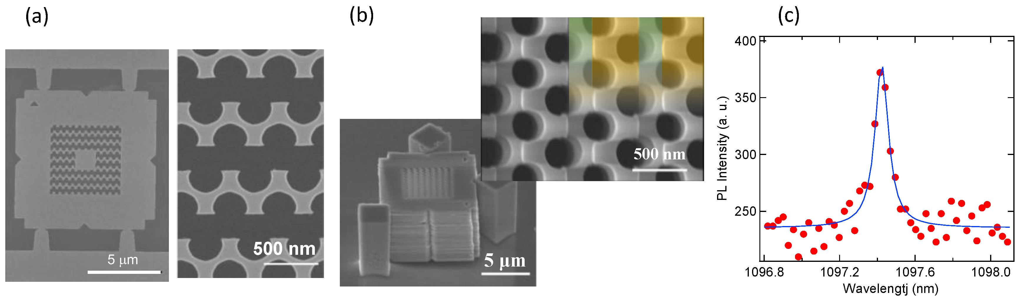
2.2. Fabrication and Optical Characterization of PhC Nanocavity <110>-Layered Diamond Structure

We fabricated a 3D PhC nanocavity in the <110>-layered diamond structure by using micro manipulation [25,26]. Firstly, using a 225-nm-thick GaAs layer epitaxially grown on a 1.5-μm-thick layer of Al0.7Ga0.3As by metal organic chemical vapor deposition, we fabricated 2D plates with the in-plane patters shown in Figure 1b. The GaAs plates were suspended in air after removing the AlGaAs layer by wet etching. The plate for the cavity was also prepared by using another GaAs layer containing three-layer-staked InAs QDs (sheet density of QDs ~1010 cm−2) at the middle. The QD emission was used as the internal probe for cavity characteristics. The ground-state emission peak from the QDs was located at around 1200 nm and the excited-state emission peak was observed at around 1130 nm. By combining the ground-state and excited-state emissions, the QD emission could cover a broad spectral range from ~1050 nm to ~1250 nm at the measurement temperature of 40 K [46]. A typical SEM image of the plate with the cavity pattern is shown in Figure 2a. These plates were cut from the substrates and picked up by a glass probe in an SEM chamber equipped with micromanipulators. Then, they were stacked on another substrate where vertical posts were separately prepared. These posts are essential for positioning the plates with high accuracy. Details of the fabrication and stacking processes can be found in previous publications [26,34]. A bird’s-eye view and top view of the fabricated sample are shown in Figure 2b. The sample has 14 plates below the cavity.
We characterized the sample by μ-PL measurement at low temperature (40 K) and found a cavity mode at around 1098 nm, close to the center of the measured PBG region. In the experiment, the cPBG region was unintentionally shifted from the design. The procedure for assigning the PBG region is described in [46]. The measured Q initially increases and starts to saturate at larger number of upper plates [46]. This is a similar trend with the calculation in Figure 1d. A high resolution μ-PL spectrum for the structure with 14 plates above the cavity is shown in Figure 2c. From curve fitting using a Lorentz function, the Q factor was estimated to be ~12,800. We also fabricated the 3D PhC nanocavity in the woodpile structure discussed in the previous subsection. The structure has the same cavity size, the same plate and pattern sizes, and the same number of plates with the sample with the <110> structure. The Q of the sample with woodpile structure is 1.2 times lower than that of the nanocavity in the <110> structure. The expected ratio from Figure 1d is ~6. The measured Qs and the resultant ratio are much smaller than the expected values. There are several factors that limit the experimental Q factors. The structural imperfection in the real samples is one of the factors. In the present experiment, we supposed that the residual absorption of embedded QDs was the main factor. The absorption caps the cavity Qs at much lower level than the calculated values and reduces the ratio (see also the discussion in [46]). The measured value in the sample with the <110> structure is not the highest Q among 3D PhC nanocavities. However, this result suggests the potential advantage of the <110> structure for realizing high Q 3D PhC nanocavity within a limited in-plane area.

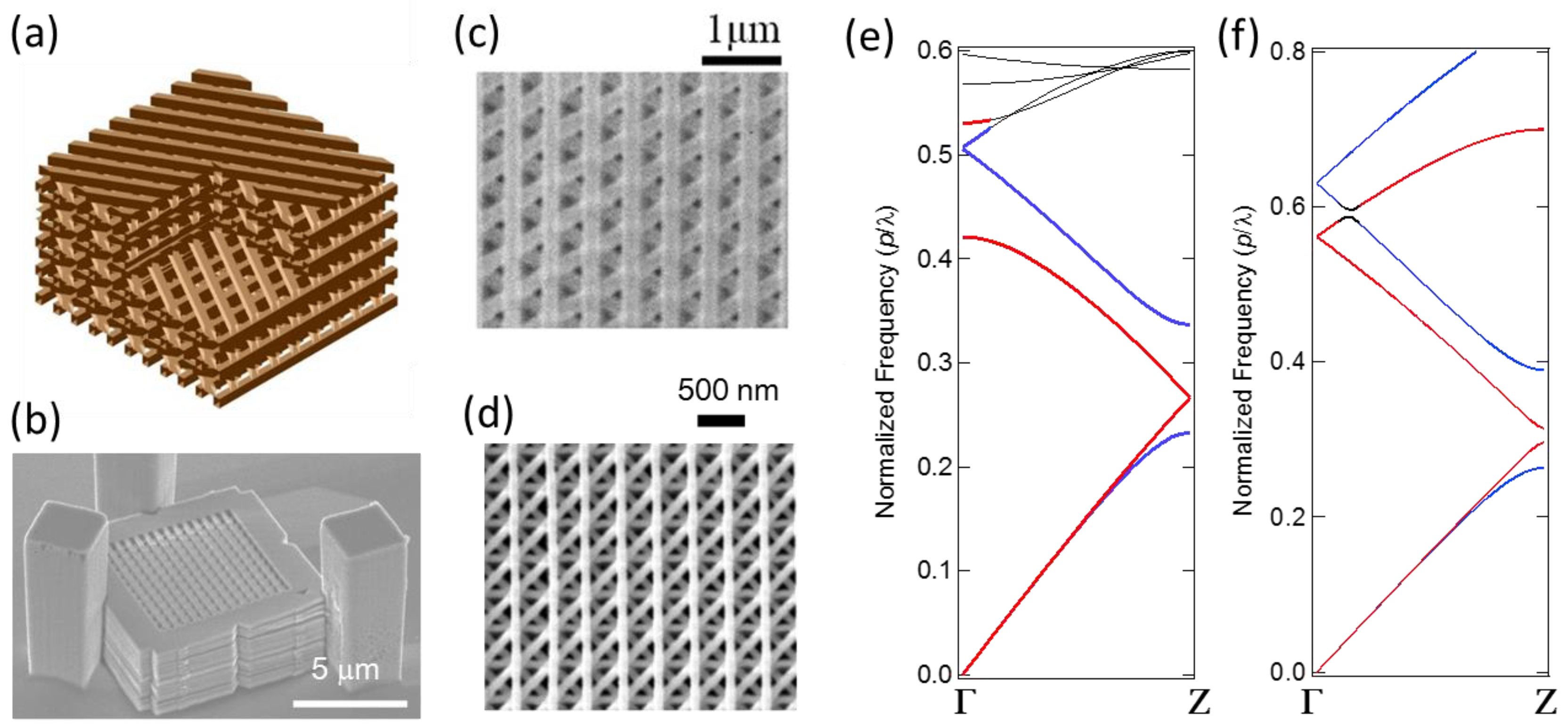
3. Artificial Optical Activity in Semiconductor Chiral Photonic Crystals

Chiral materials/structures lacking mirror and spatial inversion symmetry interact with right-handed and left-handed circularly polarized (RCP and LCP) lights differently. This difference gives a phase delay between RCP and LCP components during the propagation, which allows for the rotation of the plane of polarization for linearly polarized incident light. This phenomenon is known as circular birefringence and optical rotation. Another consequence of the CP-dependent interaction in such materials/structures is circular dichroism, which is observed as a difference in transmittance for two orthogonal CPs. Therefore, optical activity, comprised of these two effects, provides a way to manipulate CP light. CP light is used for investigating molecular chirality in the fields of chemistry, biology and medicine. In the field of quantum information technology, CP states of light plays a key role for realizing efficient interfaces between spins in solid state systems such as semiconductor QDs and photons because the optical selection rule allows to generate a spin state depending on the CP state of light [47]. Therefore, it is important to efficiently control CP lights including its efficient generation.
Optical activity in natural materials is generally weak. Therefore, much research has been devoted to enhancing optical activity by introducing artificial structures. In artificial optical nanostructures, the spatial variation of the optical electric field takes place on a wavelength scale, which makes the artificial optical activity remarkable. Enhanced optical rotation has been demonstrated using quasi-2D chiral structures [48,49,50]. Artificial 3D photonic structures, by fully utilizing the third dimension, can provide much wider and flexible platforms for manipulating CP photons including their interactions with materials. Among various structures including metallic helixes [51,52] and twisted metamaterials [53,54], chiral 3D PhCs consisting of a periodic array of chiral structures are a promising structure for realizing CP-based photonic devices. Due to the periodicity along the chiral axis, a photonic band structure for CP light is created. A PBG for the polarization that has the same chirality as the structure is also formed, which gives different transmittances for two circular polarizations, i.e., circular dichroism. CP-based photonic band structure and bandgaps facilitate manipulation of the propagation and localization of CP light, as well as control over CP light emission and thermal radiation [55] by engineering CP vacuum fields. Laser oscillation with CP output using self-assembled cholesteric liquid crystals [56,57] has been achieved. Chiral beam splitter and strong circular dichroism have also been demonstrated in polymeric materials [58,59,60].
Semiconductor materials have large refractive indices and a wide transmission window below their electronic bandgap energies. These properties will strengthen the controllability and flexibility of CP lights in semiconductor-based 3D chiral PhCs. Moreover, by introducing high-quality light emitters such as QDs, semiconductor-based structures could be used as a platform for efficient CP-light emitting devices and spin-photon interfaces [61,62] in future quantum information processing applications.

3.1. Semiconductor Chiral 3D PhCs

Figures 3a,b show a schematic illustration and a bird’s-eye-view SEM image of semiconductor (GaAs)-based chiral 3D PhCs fabricated using micro-manipulation. The structures can be categorized as “layer-by-layer” chiral PhCs [55,58]. In contrast to woodpile and <110>-layered diamond structures, the rods in neighboring plates are neither in parallel nor orthogonal. When the angle between the rods in neighboring plates is θ, 2π/θ-plates constructs a single helical unit along the stacking direction. Figures 3c,d show top views of the structures with θ = π/3 and π/4, respectively. The structures discussed in the following subsections are composed of 225-nm-thick GaAs plates. Figure 3e shows a photonic band structure along the stacked direction for the case of θ = π/3. A rod width of 160 nm and a period of 500 nm are used. The frequency is normalized by the helical pitch p = 3 × 225 nm. For comparison, a photonic band diagram for θ = π/4 is shown in Figure 3f. Here, the frequency is normalized by the helical pitch p = 4 × 225 nm. In both plots, curves colored with red and blue represent the LCP and RCP photonic modes, respectively. The band structures are basically similar to each other. Both structures have polarization gaps. For the structure with θ = π/3, they are located around p/λ = 0.28 and 0.48 in this example. In such frequency regions, strong circular dichroism appears. On the other hand, in the frequency regions where both colored bands exist, optical rotation is expected.

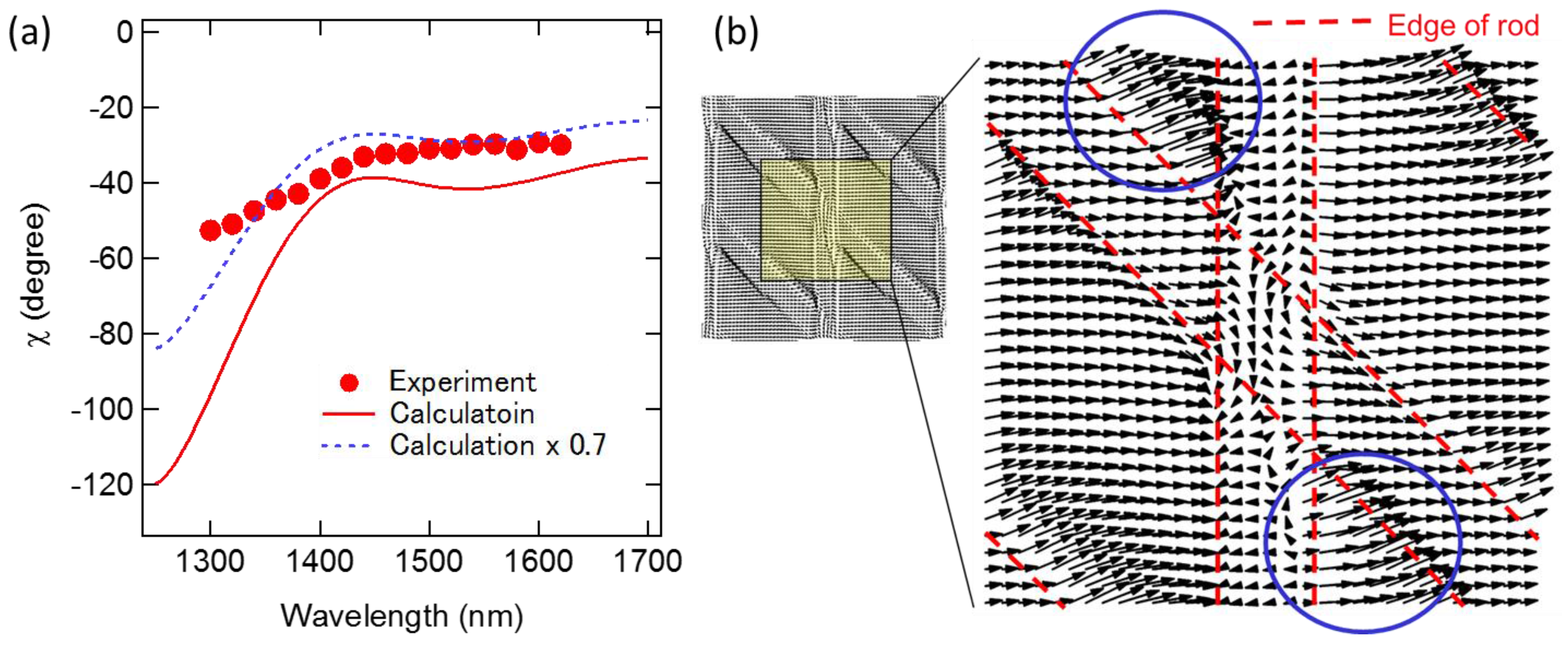
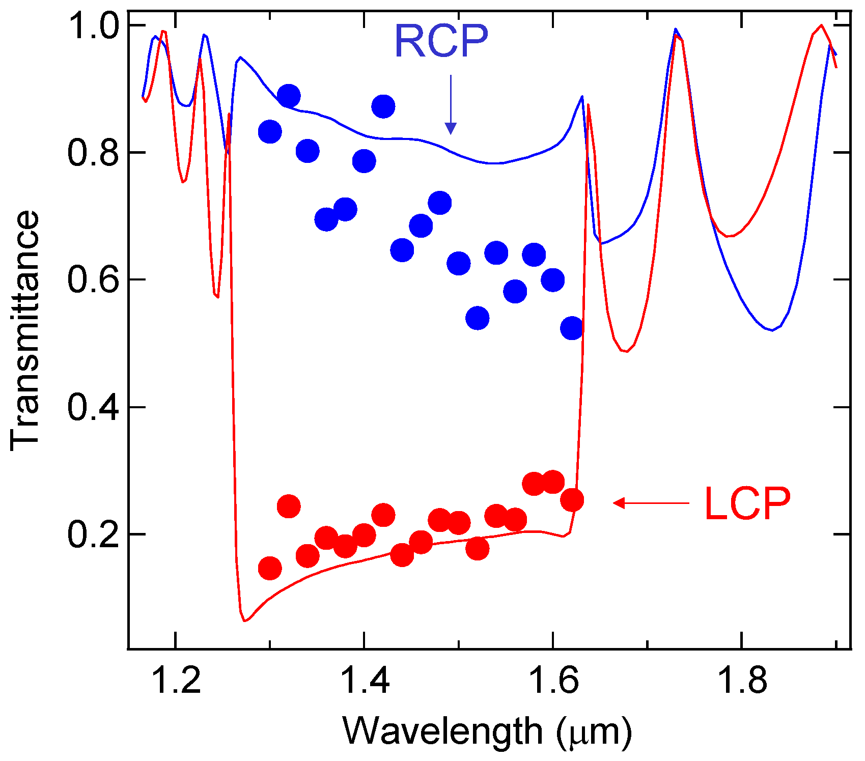
3.2. Broadband Circular Dichroism in Semiconductor Chiral 3D PhC

We fabricated a chiral 3D PhC with θ = π/3 and observed circular dichroism over a wide wavelength range covering from the O to the L telecommunication bands. The sample was constructed using 16 plates with a rod width of 160 nm. The rod period in each plate was 500 nm. We measured the transmittance of the structure along the stacked direction by using a wavelength tunable laser. The results are plotted in Figure 4 together with the transmittance spectra calculated by 3D-FDTD. In the available wavelength range of the laser (1.3~1.62 μm), the transmittance of RCP and LCP light is largely different. This result agrees well with the calculation as shown in Figure 4. The wavelength range exhibiting circular dichroism here corresponds to the polarization gap around the normalized frequency of 0.48 in Figure 3e. In a separate measurement using a broadband super-continuum laser, we also confirmed that the difference in transmitted power between incident RCP and LCP lights is small at wavelengths <1.25 μm except for the influence of the interference due to the finite thickness of the structure (see Figure 3 in [63]). The broad bandwidth of circular dichroism (circular Bragg reflection) is attributed to the large contrast in refractive index between GaAs and Air. More details, including discussions of eigenpolarization states of the structure, can be found in our previous report [63].

3.3. Enahnced Opical Rotationin a Semcionductor Chiral 3D PhC

Large optical rotation in a semiconductor chiral 3D PhC was also demonstrated. In the experiment, we used a structure with θ = π/4. Thus, four plates are needed to construct a single helical unit along the stacking direction. In the first (third) plate, the rod period is 500 nm. On the other hand, for the second (fourth) plate, the rod patterns are rotated by π/4 with respect to that in the first plate and the period is changed to 500/ 2 nm. The rod width was 100 nm in all plates. We used different period of rods in the first (third) and second (fourth) plates so that crossing points form a square lattice when viewed from above (see Figure 3d). We measured the sample with nine plates on a GaAs substrate. The total thickness of the chiral structure is approximately 2 μm.
Due to the existence of linear birefringence and linear dichroism in the structure, it is not so simple to extract the optical rotation in the experiments [49]. We analyzed the polarization state of the transmitted light along the stacked direction for a linearly polarized (LP) incident laser light from a wavelength tunable laser (1.3–1.62 μm) by measuring two parameters: the ellipticity, ϕ, of the transmitted light and the polarization rotation angle, α, defined as the angle between the LP direction of the incident laser and the major axis of the ellipse in the elliptically polarized transmitted light. ϕ and α were recorded by rotating the angle of polarization of the LP incident light at various wavelengths. From these results, we extracted the genuine optical rotation angle χ.
Figure 5a shows the experimentally obtained wavelength dependence of χ. |χ| becomes larger at shorter wavelengths. This trend qualitatively agrees with the calculated result based on 3D-FDTD, which is also plotted in the same figure. The wavelength dependence can be understood by considering the difference in wave vectors for two CP states. As the wavelength approaches 1300 nm, which corresponds to the normalized frequency of 0.69 in the band diagram (Figure 3f), the wave vector difference between two CP states becomes larger. Larger difference in wave vectors creates a larger phase difference between two CP states of light, which induces a larger optical rotation angle. On the other hand, there is a clear discrepancy in the slope at the short wavelength region in Figure 5a. The effect of finite numerical aperture of the objective lens used in the experiment and imperfections in the fabrication and experimental setup would smear the steep change in the real sample. These factors could also cause the difference between the experimentally measured and calculated values of χ.
The maximum rotation angle obtained in the present experiment is 52.5° at 1.3 μm. Considering the total thickness of chiral structure, this value corresponds to a rotation power of ~2.6 × 10⁵ °/cm, which is ~1000 times larger than in α-quartz. We also observed a large rotation angle > ~30° over the measured spectral range. The large optical rotation in the structure is explained by abrupt changes of the optical electric field at the interfaces of rods in neighboring plates. Figure 5b shows the distribution of the electric field vector calculated at the interface between the first and the second plates when linearly polarized light at a wavelength of 1400 nm is injected. The electric field changes its direction largely in small regions at around the cross points of two rods (inside the circles). The spatial dispersion of the electric field within wavelength-scale regions can be accumulated through a unit cell along the stacked direction due to its chiral nature. This induces large optical rotation effect in chiral 3D PhCs. Details on the experiment and analysis procedures, as well as other discussions, can be found in our previous report [64].

4. Summary

We have discussed the recent progress of 3D PhCs with non-woodpile layer-by-layer structures fabricated by micromanipulation. The <110>-layered diamond structure is useful for improving the cavity Q of a 3D PhC nanocavity under the condition where the available in-plane size is limited. The introduction of a chiral structure provides a novel functionality of 3D PhCs, that is, the ability to control circularly polarized light. These are some steps for expanding the frontier of 3D PhC research. On the other hand, there are many other novel structures that require investigation, and there is still room for improvement of the fabrication technology. Further development of fabrication technologies and exploration of the possibility to use novel structures are important for fully utilizing the unique properties of 3D PhCs. These progresses will pave the way for the discovery of new physics and novel applications of 3D PhCs.

Acknowledgments

The authors would like to acknowledge Y. Ota, A. Tandaechanurat, J. Tatebayashi, and S. Ishida for fruitful discussions and technical support. The authors also thank M. Holmes for his careful reading of the manuscript. This work is supported in part by JSPS KAKENHI Grant-in-Aid for Specially Promoted Research (15H05700), MEXT KAKENHI Grant-in-Aid for Scientific Research on Innovative Areas (15H05868), the Project for Developing Innovation Systems of MEXT, and NEDO project.

Conflicts of Interest

The authors declare no conflict of interest.

Abbreviations

The following abbreviations are used in this manuscript:
PhCphotonic crystal
3Dthere-dimensional
2Dtwo-dimensional
QDquantum dot
CQEDcavity quantum electrodynamics
PBGphotonic bandgap
cPBGcomplete photonic bandgap
CPcircularly polarized
RCPright-handed circularly polarized
LCPleft-handed circularly polarized
LPlinearly polarized
PLphotoluminescence
FDTDfinite-difference time domain method

References

  1. Joannopoulos, J.D.; Johnson, S.G.; Winn, J.N.; Meade, R.R. Photonic Crystals: Molding the Flow of Light, 2nd ed.; Princeton University Press: Princeton, NJ, USA, 2008. [Google Scholar]
  2. Sekoguchi, H.; Takahashi, Y.; Asano, T.; Noda, S. Photonic crystal nanocavity with a Q-factor of ~9 million. Opt. Express 2014, 22, 916–924. [Google Scholar] [CrossRef] [PubMed]
  3. Strauf, S.; Hennessy, K.; Rakher, M.T.; Choi, Y.-S.; Badolato, A.; Andreani, L.C.; Hu, E.L.; Petroff, P.M.; Bouwmeester, D. Self-Tuned Quantum Dot Gain in Photonic Crystal Lasers. Phys. Rev. Lett. 2006, 96, 127404. [Google Scholar] [CrossRef] [PubMed]
  4. Nomura, M.; Iwamoto, S.; Watanabe, K.; Kumagai, N.; Nakata, Y.; Ishida, S.; Arakawa, Y. Room temperature continuous-wave lasing in photonic crystal nanocavity. Opt. Express 2006, 14, 6308–6315. [Google Scholar] [CrossRef] [PubMed]
  5. Ellis, B.; Mayer, M.A.; Shambat, G.; Sarmiento, T.; Harris, J.; Haller, E.E.; Vučković, J. Ultralow-threshold electrically pumped quantum-dot photonic-crystal nanocavity laser. Nat. Photonics 2011, 5, 297–300. [Google Scholar] [CrossRef]
  6. Jeong, K.-J.; No, Y.-S.; Hwang, Y.; Kim, K.S.; Seo, M.-K.; Park, H.-G.; Lee, Y.-H. Electrically driven nanobeam laser. Nat. Commun. 2013, 4, 2822. [Google Scholar] [CrossRef]
  7. Prieto, I.; Llorens, J.M.; Muñoz-Camúñez, L.E.; Taboada, A.G.; Canet-Ferrer, J.; Ripalda, J.M.; Robles, C.; Muñoz-Matutano, G.J.; Martínez-Pastor, P.; Postigo, P.A. Near thresholdless laser operation at room temperature. Optica 2015, 2, 66–69. [Google Scholar] [CrossRef]
  8. Takiguchi, M.; Taniyama, H.; Sumikura, H.; Birowosuto, M.D.; Kuramochi, E.; Shinya, A.; Sato, T.; Takeda, K.; Matsuo, S.; Notomi, M. Systematic study of thresholdless oscillation in high-β buried multiple-quantum-well photonic crystal nanocavity lasers. Opt. Express 2016, 24, 3441–3450. [Google Scholar] [CrossRef] [PubMed]
  9. Arakawa, Y.; Iwamoto, S.; Nomura, M.; Tandaechanurat, A.; Ota, Y. Cavity Quantum Electrodynamics and Lasing Oscillation in Single Quantum Dot-Photonic Crystal Nanocavity Coupled Systems. IEEE J. Sel. Top. Quantum Electron. 2012, 18, 1818–1829. [Google Scholar] [CrossRef]
  10. Yoshie, T.; Scherer, A.; Hendrickson, J.; Khitrova, G.; Gibbs, H.M.; Rupper, G.; Ell, C.; Shchekin, O.B.; Deppe, D.G. Vacuum Rabi splitting with a single quantum dot in a photonic crystal nanocavity. Nature 2004, 432, 200–203. [Google Scholar] [CrossRef] [PubMed]
  11. Hennessy, K.; Badolato, A.; Winger, M.; Gerace, D.; Atatüre, M.; Gulde, S.; Fält, S.; Hu, E.L.; Imamoğlu, A. Quantum nature of a strongly coupled single quantum dot-cavity system. Nature 2007, 445, 896–899. [Google Scholar] [CrossRef] [PubMed]
  12. Englund, D.; Faraon, A.; Fushman, I.; Stoltz, N.; Petroff, P.; Vučković, J. Controlling cavity reflectivity with a single quantum dot. Nature 2007, 450, 857–861. [Google Scholar] [CrossRef] [PubMed]
  13. Ota, Y.; Ohta, R.; Kumagai, N.; Iwamoto, S.; Arakawa, Y. Vacuum Rabi Spectra of a Single Quantum Emitter. Phys. Rev. Lett. 2015, 114, 143603. [Google Scholar] [CrossRef] [PubMed]
  14. Lodahl, P.; Mahmoodian, S.; Stobbe, S. Interfacing single photons and single quantum dots with photonic nanostructures. Rev. Mod. Phys. 2015, 87, 347. [Google Scholar] [CrossRef]
  15. Vos, W.L.; Woldering, L.A. Cavity quantum electrodynamics with three-dimensional photonic bandgap crystals. In Light Localisation and Lasing: Random and Quasi-random Photonic Structures, 1st ed.; Ghulinyan, M., Pavesi, L., Eds.; Cambridge University Press: Cambridge, UK, 2015; pp. 180–214. [Google Scholar]
  16. Yablonovitch, E.; Gmitter, T.J.; Leung, K.M. Photonic band structure: The face-centered-cubic case employing nonspherical atoms. Phys. Rev. Lett. 1991, 67, 2295–2298. [Google Scholar] [CrossRef] [PubMed]
  17. Wijnhoven, J.E.G.J.; Vos, W.L. Preparation of Photonic Crystals Made of Air Spheres in Titania. Science 1998, 281, 802–804. [Google Scholar] [CrossRef]
  18. Míguez, H.; Meseguer, F.; López, C.; Blanco, Á.; Moya, J.S.; Requena, J.; Mifsud, A.; Fornés, V. Control of the Photonic Crystal Properties of fcc-Packed Submicrometer SiO2 Spheres by Sintering. Adv. Mater. 1999, 10, 480–483. [Google Scholar] [CrossRef]
  19. Schilling, J.; White, J.; Scherer, A.; Stupian, G.; Hillebrand, R.; Gösele, U. Three-dimensional macroporous silicon photonic crystal with large photonic band gap. Appl. Phys. Lett. 2005, 86, 011101. [Google Scholar] [CrossRef]
  20. Takahashi, S.; Suzuki, K.; Okano, M.; Imada, M.; Nakamori, T.; Ota, Y.; Ishizaki, K.; Noda, S. Direct creation of three-dimensional photonic crystals by a top-down approach. Nat. Mat. 2009, 8, 721–725. [Google Scholar] [CrossRef] [PubMed]
  21. Grishina, D.A.; Harteveld, C.A.M.; Woldering, L.A.; Vos, W.L. Method for making a single-step etch mask for 3D monolithic nanostructures. Nanotechnology 2015, 26, 505302. [Google Scholar] [CrossRef] [PubMed]
  22. Deubel, M.; von Freymann, G.; Wegener, M.; Pereira, S.; Busch, K.; Soukoulis, C.M. Direct laser writing of three-dimensional photonic-crystal templates for telecommunications. Nat. Mat. 2004, 3, 444–447. [Google Scholar] [CrossRef] [PubMed]
  23. Yamamoto, N.; Noda, S.; Chutinan, A. Development of One Period of a Three-Dimensional Photonic Crystal in the 5–10 μm Wavelength Region by Wafer Fusion and Laser Beam Diffraction Pattern Observation Techniques. Jpn. J. Appl. Phys. 1998, 37, L1052–L1054. [Google Scholar] [CrossRef]
  24. Noda, S.; Tomoda, K.; Yamamoto, N.; Chutinan, A. Full Three-Dimensional Photonic Bandgap Crystals at Near-Infrared Wavelengths. Science 2000, 289, 604–606. [Google Scholar] [CrossRef] [PubMed]
  25. Aoki, K.; Miyazaki, H.T.; Hirayama, H.; Inoshita, K.; Baba, T.; Sakoda, K.; Shinya, N.; Aoyagi, Y. Microassembly of semiconductor three-dimensional photonic crystals. Nat. Mater. 2003, 2, 117–121. [Google Scholar] [CrossRef] [PubMed]
  26. Aoki, K.; Guimard, D.; Nishioka, M.; Nomura, M.; Iwamoto, S.; Arakawa, Y. Coupling of quantum-dot light emission with a three-dimensional photonic-crystal nanocavity. Nat. Photonics 2008, 2, 688–692. [Google Scholar] [CrossRef]
  27. Kawakami, S. Fabrication of submicrometre 3D periodic structures composed of Si/SiO2. Electron. Lett. 1997, 33, 1260–1261. [Google Scholar] [CrossRef]
  28. Fleming, J.G.; Lin, S.-Y. Three-dimensional photonic crystal with a stop band from 1.35 to 1.95 μm. Opt. Lett. 1999, 24, 49–51. [Google Scholar] [CrossRef] [PubMed]
  29. Lourtioz, J.-M.; Benisty, H.; Berger, V.; Gerard, J.-M.; Maystre, D.; Tchelnokov, A. Three-Dimensional Structures in Optics. In Photonic Crystals towards Nanoscale Photonic Devices, 2nd ed.; Springer: Berlin, Germany, 2008; pp. 393–412. [Google Scholar]
  30. Imada, M.; Lee, L.H.; Okano, M.; Kawashima, S.; Noda, S. Development of three-dimensional photonic-crystal waveguides at optical-communication wavelengths. Appl. Phys. Lett. 2006, 88, 171107. [Google Scholar] [CrossRef]
  31. Qi, M.; Lidorikis, E.; Rakich, P.T.; Johnson, S.G.; Joannopoulos, J.D.; Ippen, E.P.; Smith, H.I. A three-dimensional optical photonic crystal with designed point defects. Nature 2004, 429, 538–542. [Google Scholar] [CrossRef] [PubMed]
  32. Ogawa, S.; Imada, M.; Yoshimoto, S.; Okano, M.; Noda, S. Control of Light Emission by 3D Photonic Crystals. Science 2004, 305, 227–229. [Google Scholar] [CrossRef] [PubMed]
  33. Ishizaki, K.; Koumura, M.; Suzuki, K.; Gondaira, K.; Noda, S. Realization of three-dimensional guiding of photons in photonic crystals. Nat. Photonics 2013, 7, 133–137. [Google Scholar] [CrossRef]
  34. Tandaechanura, A.; Ishida, S.; Guimard, D.; Nomura, M.; Iwamoto, S.; Arakawa, Y. Lasing oscillation in a three-dimensional photonic crystal nanocavity with a complete bandgap. Nat. Photonics 2010, 5, 91–94. [Google Scholar] [CrossRef]
  35. Ishizaki, K.; Noda, S. Manipulation of photons at the surface of three-dimensional photonic crystals. Nature 2009, 460, 367–370. [Google Scholar] [CrossRef] [PubMed]
  36. Ishizaki, K.; Gondaira, K.; Ota, Y.; Suzuki, K.; Noda, S. Nanocavities at the surface of three-dimensional photonic crystals. Opt. Express 2013, 21, 10590–10596. [Google Scholar] [CrossRef] [PubMed]
  37. Cao, D.; Tangaechanurat, A.; Nakayama, S.; Ishida, S.; Iwamoto, S.; Arakawa, Y. Silicon-based three-dimensional photonic crystal nanocavity laser with InAs quantum-dot gain. Appl. Phys. Lett. 2012, 101, 191107. [Google Scholar] [CrossRef]
  38. Tandaechanurat, A.; Ota, Y.; Kumagai, N.; Ishida, S.; Iwamoto, S.; Arakawa, Y. Observation of Purcell effect in a 3D photonic crystal nanocavity with a single quantum dot. In Proceeding of the IQEC/CLEO Pacific Rim Conference, Sydney, Australia, 28 August–1 September 2011.
  39. Ho, K.M.; Chan, C.T.; Soukoulis, C.M.; Biswas, R.; Sigalas, M. Photonic band gaps in three dimensions: New layer-by-layer periodic structures. Solid State Commun. 1994, 89, 413–416. [Google Scholar] [CrossRef]
  40. Hillebrand, R.; Hergert, W. Scaling properties of a tetragonal photonic crystal design having a large complete bandgap. Photonics Nanostruc. Fundam. Appl. 2004, 2, 33–39. [Google Scholar] [CrossRef]
  41. Fan, S.; Villeneuve, P.R.; Meade, R.D.; Joannopoulos, J.D. Design of three-dimensional photonic crystals at submicron lengthscales. Appl. Phys. Lett. 1994, 65, 1466–1468. [Google Scholar] [CrossRef]
  42. Maldovan, M. Layer-by-layer photonic crystal with a repeating two-layer sequence. Appl. Phys. Lett. 2004, 85, 911–913. [Google Scholar] [CrossRef]
  43. Maldovan, M.; Thomas, E.L. Diamond-structured photonic crystals. Nat. Matter. 2004, 3, 593–600. [Google Scholar] [CrossRef] [PubMed]
  44. Men, K.; Lee, K.Y.K.; Freund, R.M.; Peraire, J.; Johnson, S.G. Robust topology optimization of three-dimensional photonic-crystal band-gap structures. Opt. Express 2014, 22, 22632–22648. [Google Scholar] [CrossRef] [PubMed]
  45. Tajiri, T.; Takahashi, S.; Tandaechanurat, A.; Iwamoto, S.; Arakawa, Y. Design of ta three-dimensional photonic crystal nanocavity based on a <110>-layered diamond structure. Jpn. J. Appl. Phys. 2014, 53, 04EG08. [Google Scholar] [CrossRef]
  46. Tajiri, T.; Takahashi, S.; Ota, Y.; Tatebayashi, J.; Iwamoto, S.; Arakawa, Y. Demonstration of a three-dimensional photonic crystal nanocavity in a <110>-layered diamond structure. Appl. Phys. Lett. 2015, 107, 071102. [Google Scholar] [CrossRef]
  47. Gywat, O.; Krenner, H.J.; Berezovsky, J. Experimental Methods for Optical Initialization, Readout, and Manipulation. In Spins in Optically Active Quantum Dots; Wiley-VCH: Weinheim, Germany, 2010; pp. 111–165. [Google Scholar]
  48. Kuwata-Gonikami, M.; Saito, N.; Ino, Y.; Kauranen, M.; Jefimovs, K.; Vallius, T.; Turunen, J.; Svirko, Y.P. Giant optical activity in quasi-two-dimensional planar nanostructures. Phys. Rev. Lett. 2005, 95, 227401. [Google Scholar] [CrossRef] [PubMed]
  49. Konishi, K.; Sugimoto, T.; Bai, B.; Svirko, Y.; Kuwata-Gonokami, M. Effect of surface plasmon resonance on the optical activity of chiral metal nanogratings. Opt. Express 2007, 15, 9575–9583. [Google Scholar] [CrossRef] [PubMed]
  50. Konishi, K.; Bai, B.; Meng, X.; Karvinen, P.; Turunen, J.; Svirko, Y.P.; Kuwata-Gonokami, M. Observation of extraordinary optical activity in planer chiral photonic crystals. Opt. Express 2008, 16, 7189–7196. [Google Scholar] [CrossRef] [PubMed]
  51. Gansel, J.K.; Thiel, M.; Rill, M.S.; Decker, M.; Bade, K.; Saile, V.; von Freymann, G.; Linden, S.; Wegener, M. Gold helix photonic metamaterial as broadband circular polarizer. Science 2009, 325, 1513–1515. [Google Scholar] [CrossRef] [PubMed]
  52. Gibbs, J.G.; Mark, A.G.; Eslami, S.; Fischer, P. Plasmonic nanohelix metamaterials with tailorable giant circular dichroism. Appl. Phys. Lett. 2013, 103, 213101. [Google Scholar] [CrossRef]
  53. Decker, M.; Zhao, R.; Soukoulis, C.M.; Linden, S.; Wegener, M. Twisted split-ring-resonator photonic metamaterial with huge optical activity. Opt. Lett. 2010, 35, 1593–1595. [Google Scholar] [CrossRef] [PubMed]
  54. Zhao, Y.; Belkin, M.A.; Alu, A. Twisted optical metamaterials for planarized ultrathin broadband circular polarizers. Nat. Commun. 2012, 3, 870. [Google Scholar] [CrossRef] [PubMed]
  55. Lee, J.C.W.; Chan, C.T. Circularly polarized thermal radiation from layer-by-layer photonic crystal structures. Appl. Phys. Lett. 2007, 90, 051912. [Google Scholar] [CrossRef]
  56. Kopp, V.I.; Zhang, Z.-Q.; Genack, A.Z. Lasing in chiral photonic structures. Prog. Quantum Electron. 2003, 27, 369–416. [Google Scholar] [CrossRef]
  57. Coles, H.; Morris, S. Liquid-crystal lasers. Nat. Photonics 2010, 4, 676–685. [Google Scholar] [CrossRef]
  58. Thiel, M.; von Freymann, G.; Wegener, M. Layer-by-layer three dimensional chiral photonic crystal. Opt. Lett. 2007, 32, 2547–2549. [Google Scholar] [CrossRef] [PubMed]
  59. Thiel, M.; Decker, M.; Deubel, M.; Wegener, M.; Linden, S.; von Freymann, G. Polarization stop bands in chiral polymeric three-dimensional photonic crystals. Adv. Mater. 2007, 19, 207–210. [Google Scholar] [CrossRef]
  60. Turner, M.D.; Saba, M.; Zhang, Q.; Cumming, B.P.; Schoeder-Turk, G.E.; Gu, M. Miniature chiral beam splitter based on gyroid photonic crystals. Nat. Photonics 2013, 7, 801–805. [Google Scholar] [CrossRef]
  61. Kroutvar, M.; Ducommun, Y.; Heiss, D.; Bichler, M.; Schuh, D.; Abstreiter, G.; Finley, J.J. Optically programmable electron spin memory using semiconductor quantum dots. Nature 2004, 432, 81–84. [Google Scholar] [CrossRef] [PubMed]
  62. Gao, W.B.; Fallahi, P.; Togan, E.; Sanchez, J.M.; Imamoglu, A. Observation of entanglement between a quantum dot spin and a single photon. Nature 2012, 491, 426–429. [Google Scholar] [CrossRef] [PubMed]
  63. Takahashi, S.; Tajiri, T.; Ota, Y.; Tatebayashi, J.; Iwamoto, S.; Arakawa, Y. Circular dichroism in a three-dimensional semiconductor chiral photonic crystal. Appl. Phys. Lett. 2014, 105, 051107. [Google Scholar] [CrossRef]
  64. Takahashi, S.; Tandaechanurat, A.; Igusa, R.; Ota, Y.; Tatebayashi, J.; Iwamoto, S.; Arakawa, Y. Giant optical rotation in a three-dimensional semiconductor chiral photonic crystal. Opt. Express 2013, 21, 29905–29913. [Google Scholar] [CrossRef] [PubMed]
Figure 1. (a) Schematic illustration of a <110>-layered diamond structure containing a square-shaped nanocavity, where top layers are partially cut for showing the cavity area. The right figure is a magnified image of the cavity area; (b) In-plane patterns of the plates to be stacked (left), and top (right top) and cross sectional (right bottom) views of the <110>-layered diamond structure; (c) Photonic band diagram of the structure. The colored region indicates cPBG. The Brillouin zone is illustrated in the inset; (d) Calculated Q of the nanocavities in <110>-layered diamond (red dots) and woodpile (blue dots) structures as a function of number of plates above the cavity. The inset shows the electric field energy distribution of the cavity mode in <110>-layered diamond structure.
Photonics 03 00034 g001
Figure 2. (a) SEM image of a plate with cavity structure (left) and a magnified image of the fabricated rod pattern; (b) Bird’s-eye view and top view of a 3D PhC nanocavity with the <110>-layered diamond structure. The colored areas in the top view represent two different layers shown in Figure 1b; (c) High-resolution μ-PL spectrum for 3D PhC nanocavity with 14 plates both above and below the cavity. The blue curve is the fitting curve using a Lorentz function.
Photonics 03 00034 g002
Figure 3. (a) Schematic of a layer-by-layer chiral 3D PhC; (b) SEM image of a fabricated chiral 3D PhC; (c,d) Top views of the chiral PhCs with θ = π/3 and π/4, respectively; (e,f) Photonic band diagrams for chiral PhC structures with θ = π/3 and π/4, respectively. Red and blue curves represent LCP and RCP bands.
Photonics 03 00034 g003
Figure 4. Transmittance spectra for RCP and LCP lights. Blue (red) curves and balls show the calculated and experimentally obtained spectra, respectively.
Photonics 03 00034 g004
Figure 5. (a) Optical rotation angle as a function of wavelength. The Red dots and red curve indicate the experimental results and calculated spectrum, respectively. The blue dashed curve shows the calculated spectra scaled by a factor of 0.7; (b) Electric field distribution at the interface between the first and the second plates of the chiral 3D PhC at a wavelength of 1400 nm.
Photonics 03 00034 g005

