1. Introduction
Since the first demonstration [
1] of the quantum cascade laser (QCL) over two decades ago, the surrounding technology has vastly improved, as proven by room temperature continuous wave (CW) operation [
2], high optical power [
3], low dissipation devices [
4,
5,
6], and extended accessible spectral range [
7,
8,
9,
10,
11]. These achievements can unambiguously be attributed to the extensive work on fabrication and design strategies with the aim to optimize thermal transport in the structures, to reduce the electrical footprint of the active waveguide, to decrease electrical and scattering losses due to an improved material quality, while simultaneously amplifying the power [
12,
13,
14,
15,
16,
17], as well as to continued optimization of the quantum cascade structure serving as the gain medium in QCLs [
18,
19,
20,
21,
22].
In this mature field, the present-day direction of research is to address the requirements of potential applications, such as trace gas spectroscopy [
23,
24,
25], defense countermeasures [
26,
27,
28], micro-surgery [
29,
30], and optical free-space communication [
31,
32,
33]. These technologically-challenging implementations typically call for a precise and stable mode control, high efficiency, and good beam shape. In this short review, we summarize the recent achievements in the areas of QCL fabrication at ETH Zurich and update recent results with the latest experimental data.
The paper is organized as follows: in
Section 2 we summarize our work on active region growth and highlight the tools we use for their characterization. In
Section 3 we discuss our efforts to optimize the waveguide fabrication.
Section 4 treats the different epitaxial regrowth steps in the fabrication process, and the doping engineering performed to optimize them. In
Section 5 we implement all optimizations and show our results on low dissipation short-wavelength QCLs with excellent mode control. In
Section 6 we apply a mode control strategy to fabricate multi-wavelength QCL arrays and demonstrate how a monolithically bonded collector chip can combine the different wavelengths in a single beam of light. In
Section 7 we then present an alternative device concept that allows the emission of few wavelengths together or independently without the need to bond an additional chip for the light collection.
Section 8 then describes our efforts on fabricating buried photonic crystal QCLs. We then conclude our results in
Section 9.
2. Active Region Growth and Material Characterization
First and foremost, the performance of QCLs is strongly dependent on the active layer, from which the light is emitted. One of the main aspects in realizing efficient QCL active regions is a rigorous control of the molecular beam epitaxy (MBE) growth process. A good control of the active region growth can be achieved by an adequate mixture of characterization techniques covering both global and local resolution. Here, the term “global” refers to length scales ranging from 100 µm to 1 cm, a high degree of information averaging over more than one dimension, resulting in a good sensitivity. The term “local” refers to length scales ranging from 1 Å to 10 µm and information averaging over one dimension, at most, resulting in a limited sensitivity. The typical instrumentation used for this purpose is listed in
Table 1 and is qualitatively assessed with respect to its capability to deliver a specific type of information on the respective length scale.
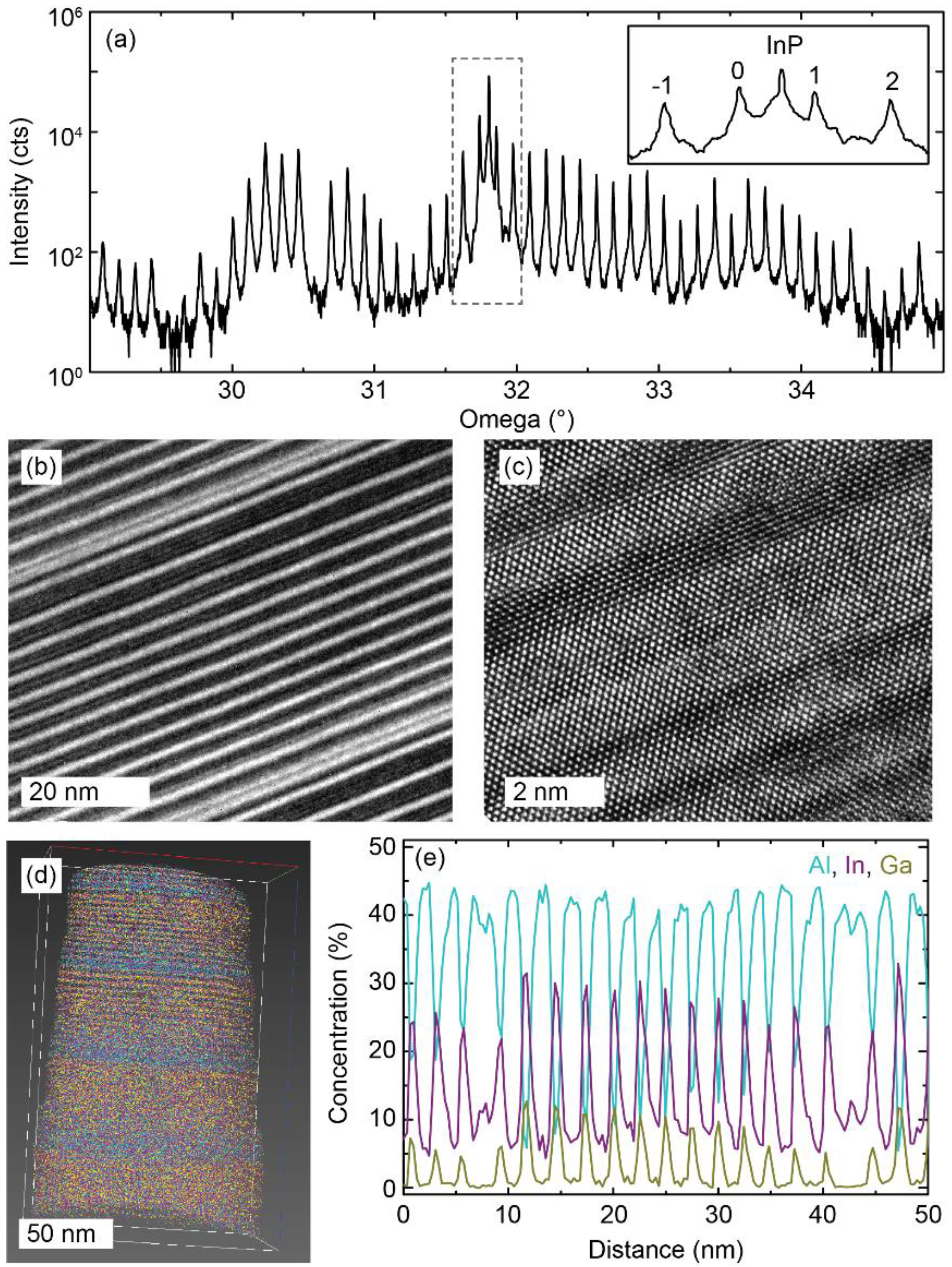
Figure 1 contains a collection of data recorded with laboratory X-ray diffraction (XRD), transmission electron microscopy (TEM), and atom probe tomography (APT) for an active region operating around 3.1–3.3 µm. The XRD measurements (
Figure 1a) disclose global information, such as the average periodicity of the active region over the whole wafer, average alloy concentrations, as well as deviations from center to border of the wafer and the beginning to end of the growth; e.g., from the position of the 0th order superlattice peak relative to the substrate peak, it can be determined, whether strain relaxation has occurred during the growth. Additionally, from the spacing of the superlattice peaks, the total period thickness can be determined and compared to the designed period thickness. Complementarily, TEM measurements can resolve the superlattice with high local magnification, even down to the atomic scale (
Figure 1b), and reveal the local morphology (e.g., interface roughness) of the layers (
Figure 1c).
Chemical information can be obtained by APT measurements, which can deliver the three-dimensional distribution of chemical species (
Figure 1d). This is of particular interest when segregation or depletion of particular elements is studied, and the location and size of the resulting clusters are of interest. On the other hand, if the epitaxial growth is of very high quality, this representation of data can be used e.g. for determination of the chemical roughness of interfaces. Quantitative information about the local concentration of the different elements in growth direction can be found in averaged chemical profiles (
Figure 1e) extracted from the three-dimensional datasets (
Figure 1d). Such profiles are similar to secondary ion mass spectroscopy data but are limited in sensitivity to ppm levels. In general, the data retrieved from these measurements deliver valuable information for the adjustment of the fractional concentration of indium, gallium and aluminum, which is crucial for structural properties, such as strain balancing and interface quality, as well as electronic properties, such as band offsets and discontinuities.
3. Waveguide Fabrication
In addition to the active region design, the QCL performance depends on the implementation into a waveguide structure, which is responsible for efficient current driving in the structure and the build-up of the optical modes. Since QCLs are specifically interesting for spectroscopic applications, the desirable performance attributes are precise mode control, low power dissipation, and high slope efficiency, as well as continuous wave operation. In order to achieve these characteristics, the processing of the waveguide has to be developed carefully. In this section we will use the term “standard” to denote typical inverted buried heterostructure (iBH) process steps [
34], and the term “optimized” to denote process steps that have been modified to address the aforementioned requirements.
Starting from an active region layer, the first step in an iBH process [
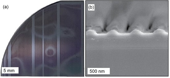
34] for single-mode devices is the photolithographic definition and wet-chemical etching of the DFB grating (
Figure 2a). For short wavelength emission (e.g., 3.3 µm) the size of the smallest grating features (260 nm) is close to the illumination wavelength (220 nm) of the mask aligner, as shown in the scanning electron microscope (SEM) image in
Figure 2b. Optical lithography steps with such narrow features are susceptible to inhomogeneous contact between the mask and sample. The resulting Newton’s rings (
cf.
Figure 2a) disrupt the grating pattern and result in modified emission wavelengths or parasitic modes in the final device. In order to minimize such effects in this lithography step, we use a diluted resist (AZ1505:EBR = 1:4), resulting in a resist thickness of 70 nm. The resist layer was exposed with a dose of 7 mJ/cm
2 on a Deep-UV mask aligner (ABM Inc., Scotts Valley, CA, USA) operating at 220 nm. The exposed resist was developed with a diluted KOH solution (1 M KOH:H
2O = 1:8) for 35 s.
In the next process step, the active core is obtained via an oxide hard mask and a wet etching step. The etching of the active waveguide requires an etchant which isotropically etches InP and the QC active region composed of ternary InGaAs and AlInAs alloys. This requirement is also necessary to provide a smooth active waveguide profile for the lateral MOVPE regrowth (discussed in the next section). In the standard iBH process HBr:HNO
3:H
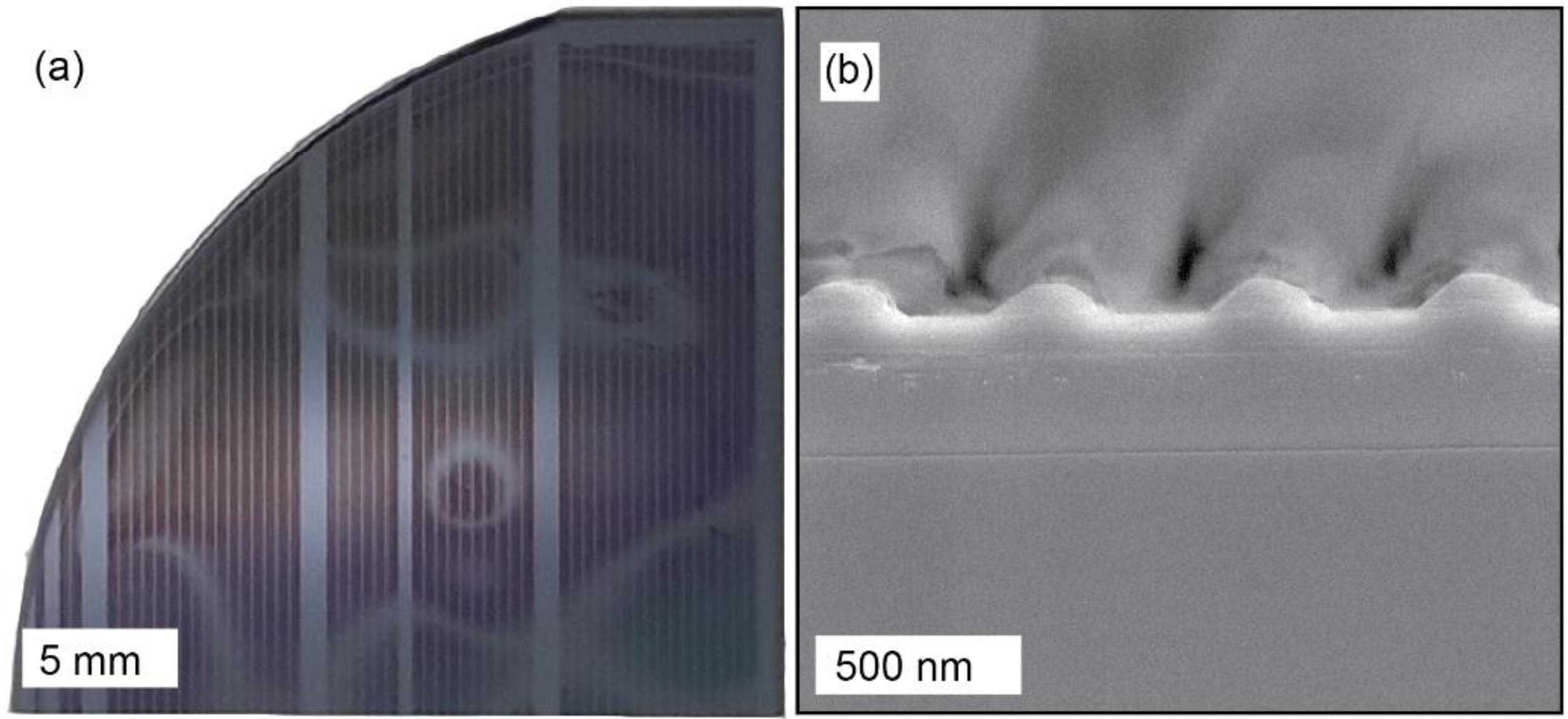
2O (1:1:10) is used for this etch step. This etchant requires an “aging” period of 10–14 days and is sensitive to visible and ultraviolet light, which can easily result in an unbalanced material selectivity. Such an imbalance can result in etch profiles at the edge of the active region featuring an unwanted sidewall roughness, as can be seen in
Figure 3a,b. The structures displayed in
Figure 3a,b were covered with an oxide to enhance the contrast for the TEM micrographs and to highlight the roughness created through this etch step. When such structures are overgrown with MOVPE, the roughness can in turn lead to the occurrence of stacking faults during regrowth (indicated with red arrows in
Figure 3c,d), which can deteriorate the electrical properties of the regrowth, by creating electrical leakage paths.
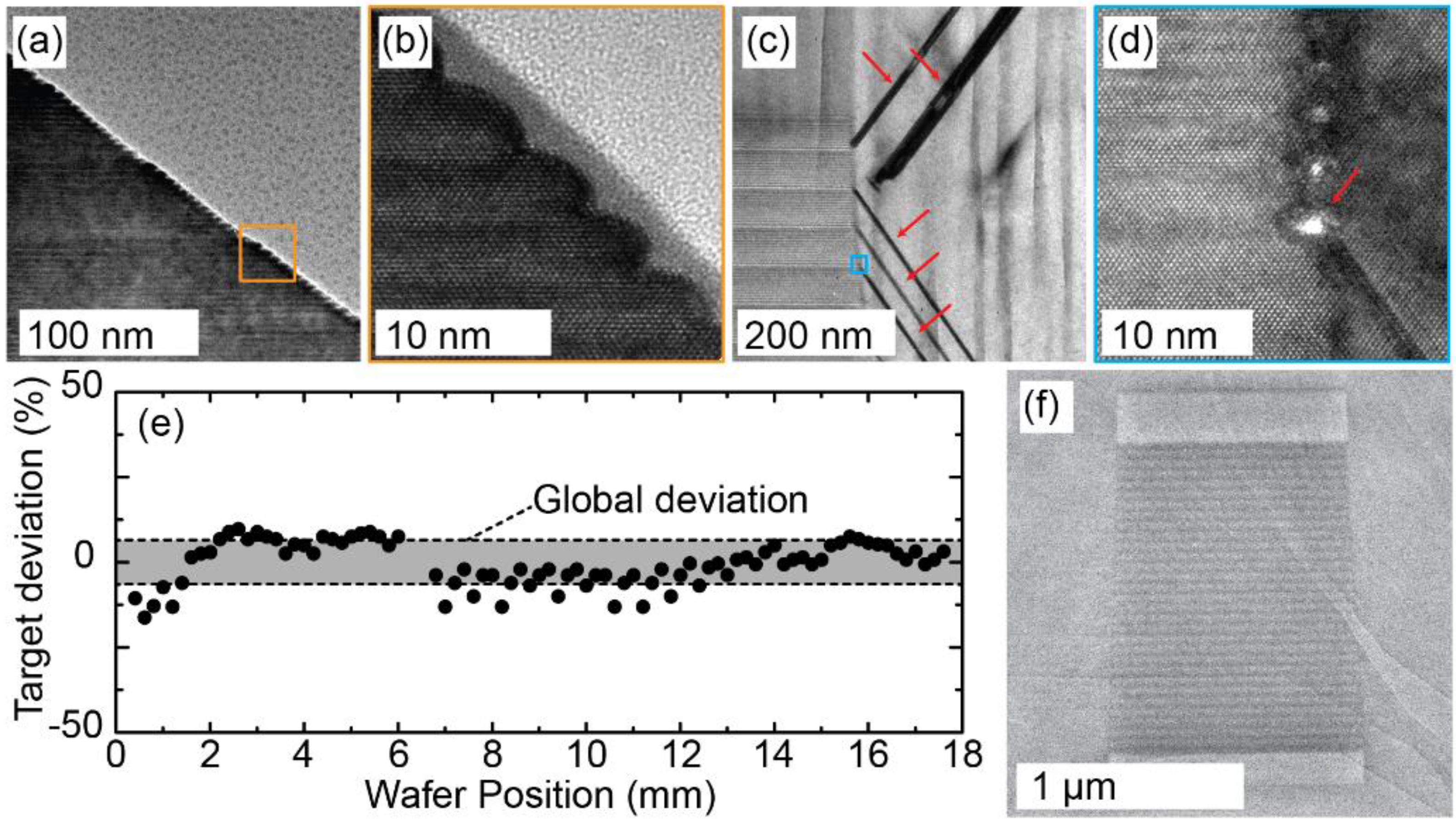
To optimize this etch step we use a diffusion-limited etching mixture of HBr:Br:H
2O (17:1:10), which provides a uniform, fast, and deep etching with smooth side walls, and creates a sufficiently large overhang of the oxide mask required for the selective MOVPE regrowth. Additionally, the width of the active waveguide can be controlled within a maximum deviation of 20% (
Figure 3e), which enables the fabrication of narrow waveguides required for low dissipation devices and a better prediction of the effective refractive index of the lasing mode, which is beneficial for precise mode control. Furthermore, sufficiently long etching can yield a rectangular shape of the active region (as opposed to a trapezoidal shape). In
Figure 3f, we show an active region of 30 active periods (layer contrast) sandwiched between two InGaAs claddings, after optimized etching, including lateral and cladding MOVPE regrowth. Since, in such rectangular shaped active cores, each period of the quantum cascade has a similar width, the current distribution is more uniform, which results in a similar alignment voltage for each period. Consequently, the overall device performance improves.
4. Epitaxial Regrowth
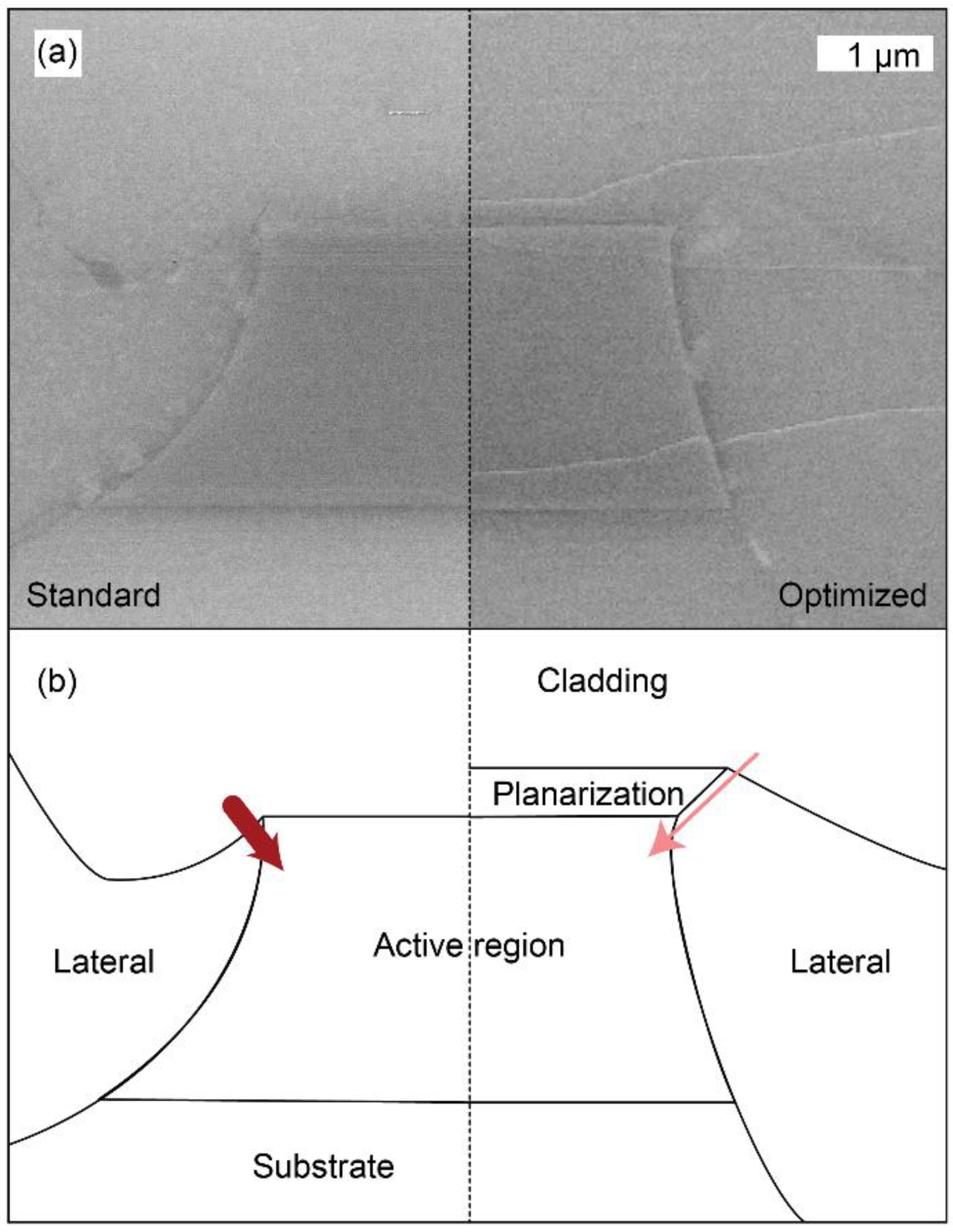
Typically, an iBH process foresees two metal-organic vapor phase epitaxy (MOVPE) regrowth steps: one regrowth to laterally insulate the active region from leakage currents (“lateral”), and a second regrowth acting as an optical cladding with minimized free carrier absorption, while reducing electrical barriers for proper injection of electrons into the active region (“cladding”). However, the material thickness of the lateral regrowth is limited by the orientation-dependent growth rate and the transport of gaseous precursor species to the side of the active core. The overhanging oxide hard-mask needed for the selective growth, and the etch profile of the active core can result in a reduced material thickness close to the upper edges of the active region. In this case the material thickness is thin enough to allow carrier tunneling through the interface between the active region and the lateral regrowth resulting in an insufficient electrical insulation. In order to reduce these leakage paths, the thickness of the insulating regrowth is increased by adding a further regrowth after the wet etching of the grating and before the definition of the active core (“planarization”), and is effectively turning the iBH process into a buried iBH process (BiBH). The planarization regrowth shares the requirements of the cladding and therefore needs to be electrically conducting while having a low enough doping to reduce free carrier absorption. SEM micrographs of the facets of a device with and a device without the planarization regrowth are compared in
Figure 4a. The two images are schematically redrawn in
Figure 4b, in order to indicate the increased material thickness of the lateral regrowth close to the active region due to the planarization regrowth. The red arrows schematically indicate the potential magnitude of leakage currents into the side of the active region due to tunneling, which is expected to be lower in the case of an additional planarization regrowth.
The lateral electrical isolation of the active region is crucial for the final device performance and is usually achieved by a Fe-doped (6 × 10
16 cm
−3) InP selective regrowth. The Fe dopants act as mid-gap traps for free carriers and, thus, pin the Fermi level in the forbidden bandgap at the interface between n-InP and Fe:InP, effectively blocking electronic current through this interface [
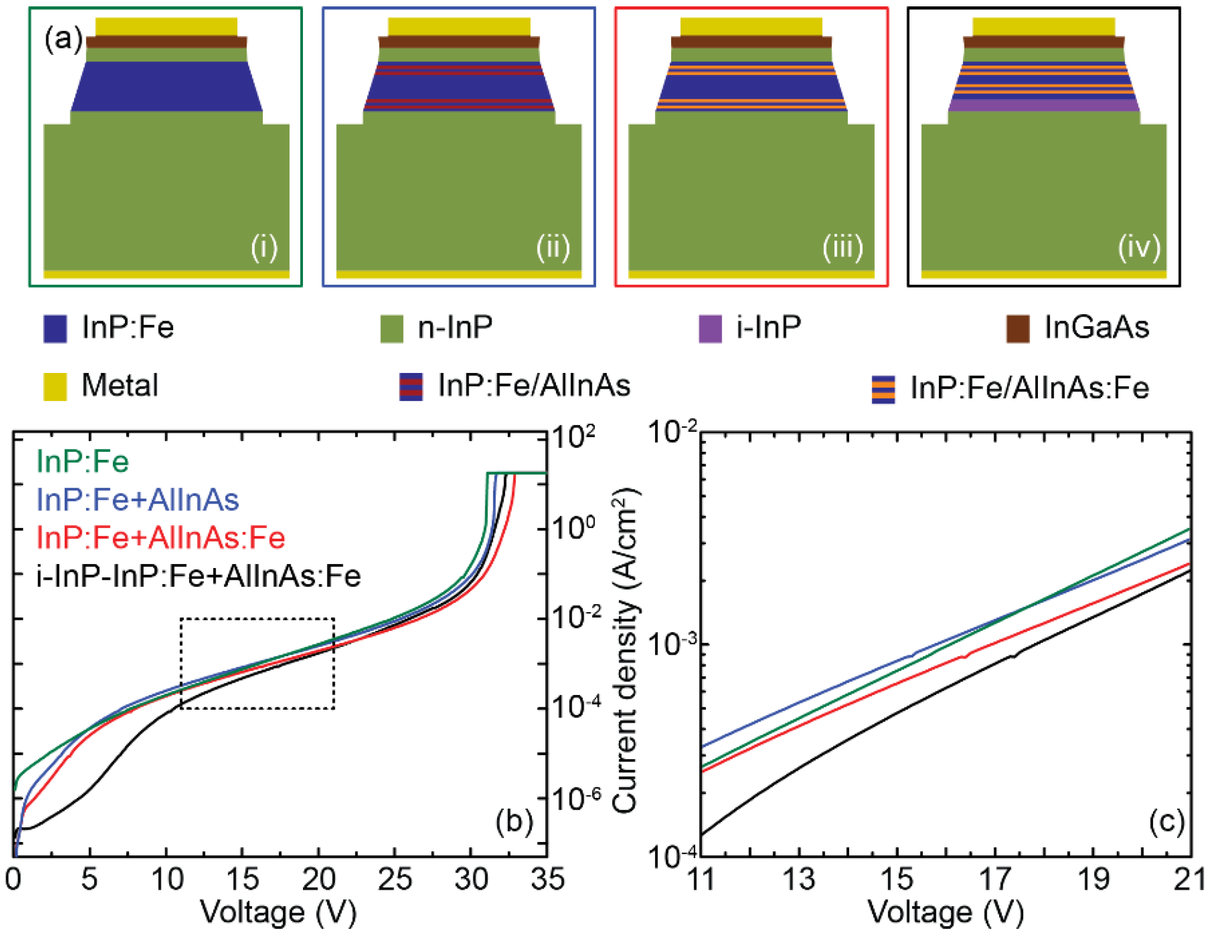
12]. One potential leakage path is bulk leakage due to an insufficiently high Fe-doping concentration in the isolation regrowth. Current leakages can be detrimental for high-performing devices, since they increase the current threshold and add additional power to be dissipated which, in turn, increase the internal temperature and further deteriorate the performance. In order to further increase the resistivity of the lateral regrowth we investigated the effects of additional barriers made from AlInAs. The higher conduction band offset of this alloy increases the barrier height at the interface with InP and, thus, reduces the tunneling rate of electrons. This strategy to increase the resistivity was implemented through the introduction of a pair of 20 nm thick AlInAs layers, separated by a 50 nm thick InP layer, grown at the beginning and at the end of the lateral regrowth. The four different material configurations investigated were (i) pure InP:Fe as a reference; (ii) InP:Fe with AlInAs barriers; (iii) InP:Fe with AlInAs:Fe barriers; and (iv) an intrinsic InP layer followed by InP:Fe with AlInAs:Fe barriers (
Figure 5a). The aim of the latter configuration is to additionally reduce photon reabsorption close to the active region in short-wavelength QCLs. The thickness of the doped InP:Fe core was 1.8 µm in structure (i–iii) and 950 nm in structure (iv), where the i-InP was 850 nm thick. These layers were processed into square mesas with an n-InP cladding (2 × 10
18 cm
−3), an InGaAs top termination layer (2 × 10
19 cm
−3), and metallic top and bottom electrode. I-V profiling was performed to assess the resistivity at different voltages (
Figure 5b,c). The voltage region most interesting for QCLs is highlighted in
Figure 3c. The best performance is achieved by layer (iv) with an additional i-InP layer, followed by layer (iii), which features (as layer (iv) as well) AlInAs:Fe barriers. Layer (ii) with undoped barriers has similar performance to the reference InP:Fe (layer (i)).
Although in these particular experiments layer (iv) showed the best performance, it should be mentioned that in practice QCLs fabricated with layer (iii) show better results. Unfortunately, the benefit of reduced optical losses through the introduced i-InP layer is handicapped by electrical leakage. Finally we want to point out, that these results are strongly dependent on a well-controlled growth process in terms of material and gas purity, growth selectivity, and crystal conformity. QCLs are particularly prone to negative influences on crystal quality, due to the increased number of interfaces and switching between material systems.
For some specialized applications the regrowth of insulating Fe-doped InP can be performed using Hydride Vapor Phase Epitaxy (HVPE). Especially, structures where growth in high-aspect-ratio crevices (e.g., photonic crystals) is required, the regrowth technique should satisfy specific considerations. Firstly, the Fe concentration should be sufficiently large to impart semi-insulation to InP,
i.e., to pin the Fermi level near the mid bandgap of InP. This is particularly important in QCLs, since the electric fields in QCLs are in general very high (e.g., compared to interband lasers). The urgency of good electrical insulation further increases when high-aspect ratio crevices are deeply etched through the active region by an ICP process. Additionally, the actual Fe concentration in layers regrown in high-aspect-ratio crevices can depend on the growth rate and the orientation, and be different compared to growths on planar substrates (due to the orientation dependent doping [
35]). Secondly, the regrowth should be selective, yield very good planarization and insensitive to the orientation of the etched mesas, to profile variations of the etched mesas (or pillars) caused by variation in process control. Finally, the regrowth should not result in appearance of crystal growth artifacts (e.g., “rabbit ears”) near the mesa (or pillar) edges [
36]. HVPE is a technique that can meet all these demands [
37].
The final regrowth step before the back-end processing of the metallic electrodes is a Si-doped InP cladding, which assures the uniform injection of carriers into the active region and, at the same time, guides the lasing modes with minimized optical losses. Engineering of the doping profile in this regrowth can provide additional shielding from leakage currents, while preserving its optical qualities. If the previously-mentioned planarization regrowth is terminated with a highly-doped (1 × 1017 cm−3) layer (40 nm), the doping at the beginning of the cladding layer can be kept relatively low (1 × 1016 cm−3). In addition, minimizing the free carrier absorption, the effect of this doping profile is that material along the lateral regrowth will be depleted and carriers will be effectively funneled through the highly-doped contact layer prevailing only on top of the active region, thus, further reducing leakage through the Fe-doped InP regrowth. Closer to the metallization layer for the electrode contact the doping can be increased (3 × 1018 cm−3) to reduce the Schottky barrier at the interface between the top electrode and the cladding regrowth.
5. Optimized DFB-QCL Performance
In this section we apply the consideration of the previous section on short wavelength QCLs to benchmark the optimized process against the standard one. QCLs at short wavelengths are particularly interesting for spectroscopic applications, since the fundamental roto-vibrational transitions of many hydrocarbons and low-molecular species are in the 3–5 µm range [
6]. At the same time, low dissipation devices with high power are desirable, because these attributes would enable field-deployable operation of the devices. However, the development of QCLs on InP in this region is challenging, because the band offset between well and barrier required to achieve radiative intersubband transitions at a high enough energy can only be achieved in antimonide-based material systems or in the strained InGaAs/AlInAs material system [
38,
39,
40,
41]. We have previously published results of lasing action in the 3 µm range [
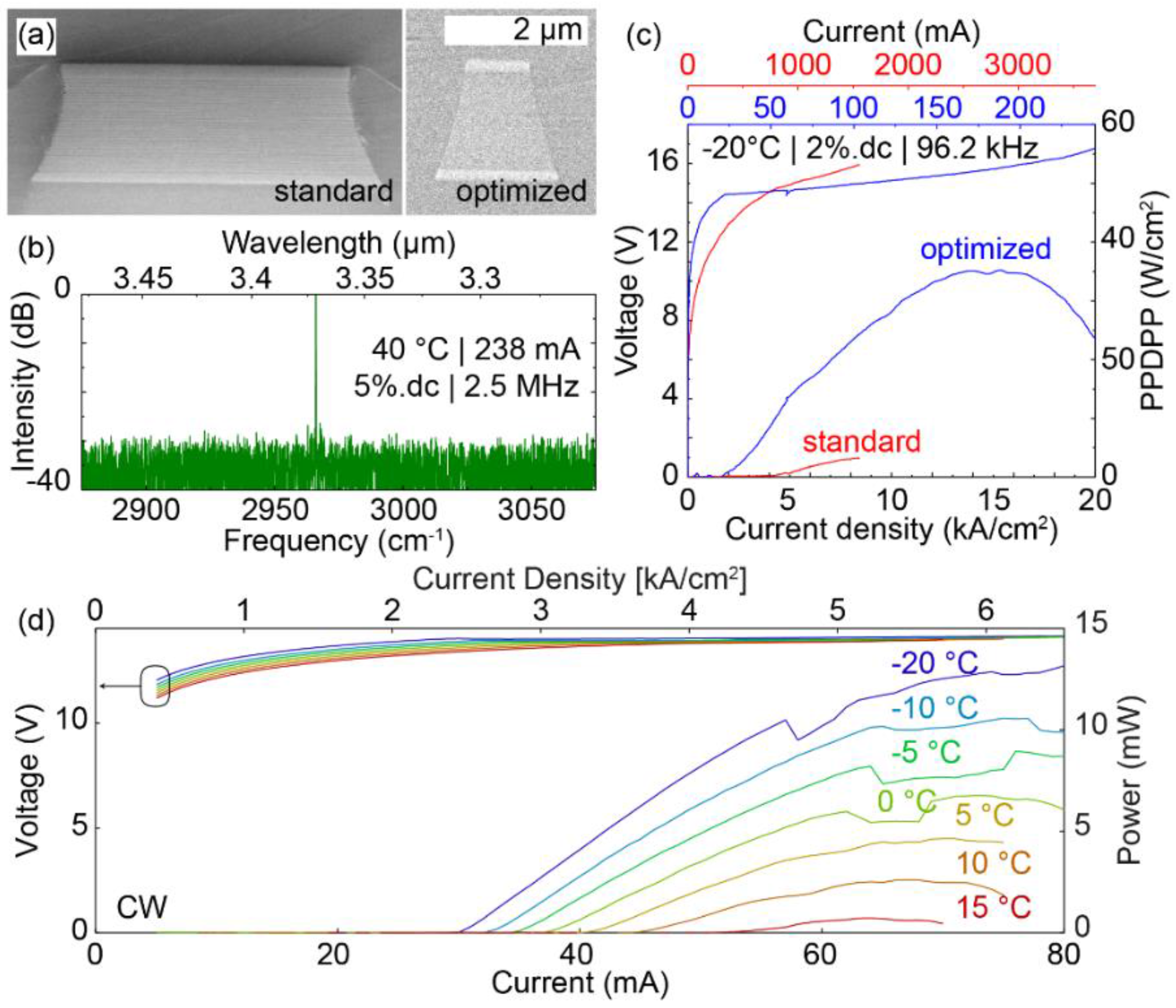
42]. In that work the device performances were impaired due to an unbalanced active region with an average 1.2% excess of indium and poor regrowth quality, resulting in leakage, high-threshold current densities, and mediocre power per QC period. Implementing the fabrication improvements described in the previous section yielded devices with narrow active waveguides, compared to previous works (
Figure 6a). The improved grating fabrication step allows these devices to operate single mode at about 3.37 µm [
6] with a side mode suppression ratio (SMSR) better than 25 dB (
Figure 6b). In
Figure 4c a device with standard active region and fabrication is compared to an optimized version. The device sizes were 2.6 mm × 7 µm (standard) and 0.6 mm × 2 µm (optimized). The optimized device shown in
Figure 4c is operating at half of the threshold current density compared to the standard device and its threshold current is as low as 25 mA.
For the comparison of lasers from different growths, processes, and size we introduce the peak power density per period PPDPP parameter. The normalization area the PPDPP parameter refers to is the planar area of the active core. The facet area is taken into account through the normalization by the amount of active periods. The PPDPP of the optimized device reaches values of more than 35 W/cm
2, whereas the standard device reaches only approximately 5 W/cm
2. Although the PPDPP parameter neglects the precise shape of the active region, mirror losses, coupling related effects, and overlap factors, the comparison shown in
Figure 6c is still convincing, because the optimized device giving rise to this data is shorter (associated with higher mirror losses) and narrower (associated by lower overlap factor) than the standard device. Additionally, a kink in the current-voltage curve (indicative for photo-induced current) and the large dynamic range (~10:1) of the optimized device is underlining the performance gains achieved by the improvements made in the active region design and processing steps. Furthermore, the application of a metallic and dielectric high-reflection coating on the back and the front facet, respectively, enables the devices from the optimized process to operate in CW up to 15 °C and with output power in the range of 10 mW (
Figure 6d). The current voltage characteristics show again characteristic kinks at the lasing threshold, a clear sign for photo-induced current. The data at currents below 4 mA is not shown because the high stability current driver used for this measurement (QCL2000, Wavelength Electronics, Inc., Bozeman, MT, USA) produces an open-circuit error for current below this threshold value.
6. QCL Arrays
For most spectroscopic applications (e.g., direct absorption measurements) reaching high power is of secondary concern and the primary interest is the ability to target absorption lines in different spectral locations simultaneously. A convenient but challenging way to achieve this goal is the monolithic integration of laser arrays on a single chip. An array of lasers arranged side by side can operate with completely isolated lasing cavities. However, it suffers from spatial separation of the light sources, and requires an external beam combination scheme [
43,
44,
45]. Although such arrays can be operational, the spectroscopic requirements for low concentration gas sensing are very stringent and are best implemented with a single source coupled into an amplifier (e.g., a multi-pass interaction cell [
46,
47]).
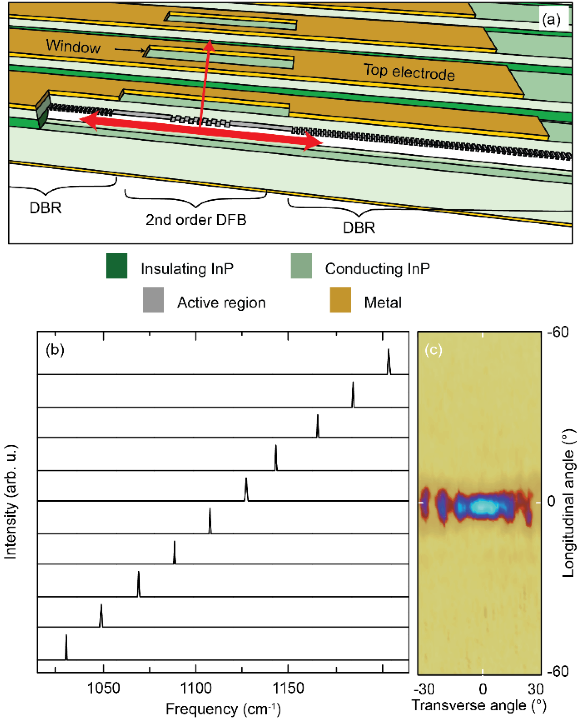
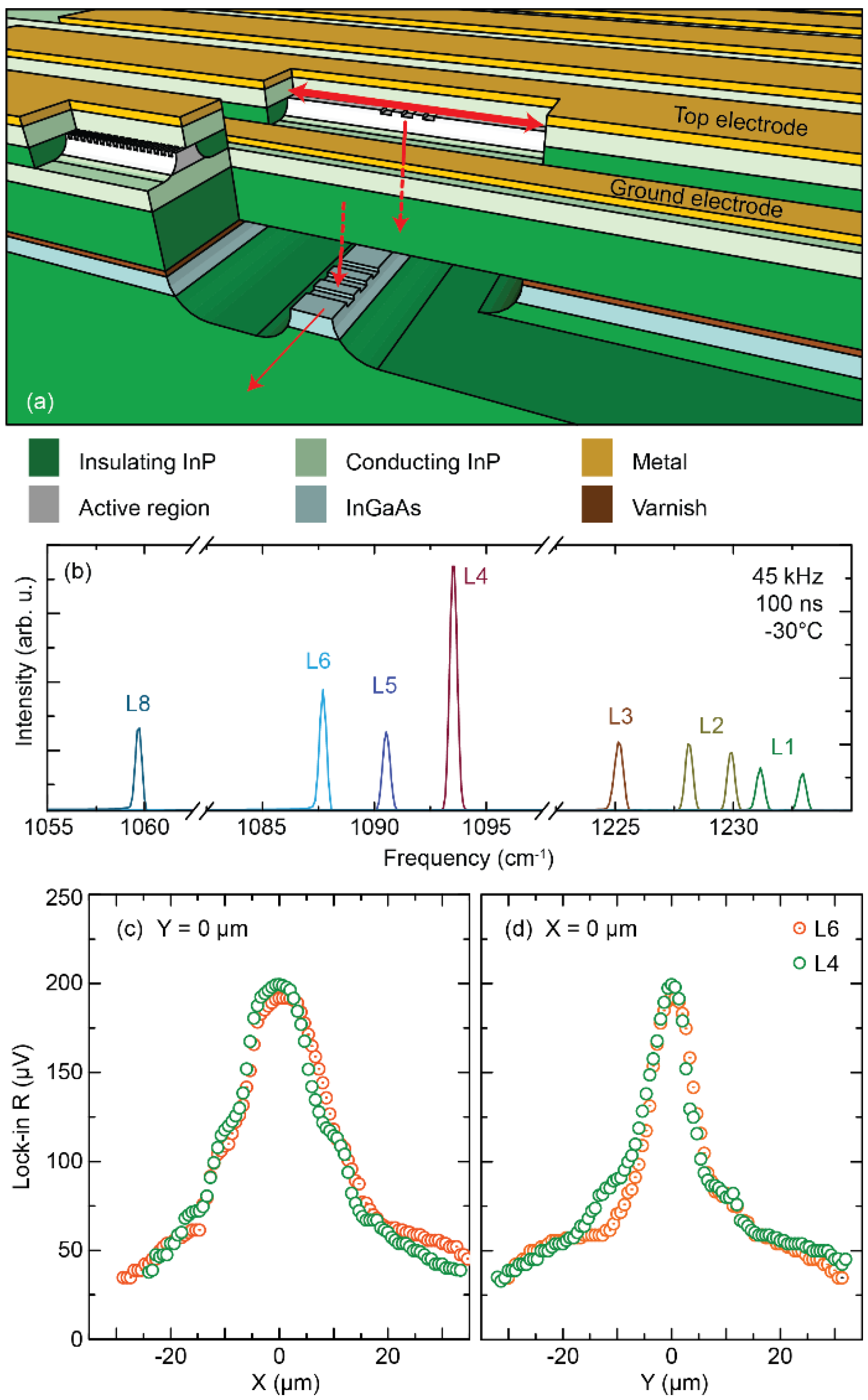
Recently, we presented a surface emitting QCL array, which features regularly spaced single mode devices with a spectral coverage of 175 cm
−1 [
48]. The mode selecting cavity is based on distributed Bragg reflectors (DBR) with a second order extractor (
Figure 7a). The distance between these two components was chosen in such a way to create a quarter wave shift defect mode in the center of the DBR stopband, allowing for a precise determination of the wavelength and, thus, a regular spectral spacing in the mode array. Additionally, we are introducing losses to the DBR sections, by only partly pumping them. This strategy helps to reduce the mode intensity at the facets, which effectively immunizes the mode selection process from the phase relation between the mode and the reflection at the facet. A chirp was introduced to the extractor grating in order to minimize the appearance of side lobes in the far-field. The radiation is emitted through a window in the top electrode. The resulting devices are arrays of 10 lasers, from which 9 out of 10 hit the desired mode (
Figure 7b), with a SMSR better than 20 dB. Narrow far-field patterns (
Figure 7c) confirm the functionality of the second order grating extractor with only few fringes originating from the metallic top contact.
The main advantages of such laser arrays are the amount of wavelengths per device area and the immunization of the mode from facet reflections. Nonetheless, the light sources are spatially separated, which will result in divergent beam paths when used in optical setups. Actual applications profit most from combined multi-wavelength beams, and thus such devices require an external beam combination scheme. Ideally, lasers emit a single beam with switchable wavelength, thus we monolithically integrated a beam combiner into the device. For this purpose we modified the previously mentioned laser array to emit the laser light through the substrate. These devices are identical to the ones presented in
Figure 7a, besides the absence of the windows in the top electrode and the relocation of the ground contact to the top surface of the chip (
Figure 8a). For the purpose of relocating the ground electrode, an additional layer of conducting InP was grown on intrinsic InP before the MBE active region growth. This layer is exposed later in the fabrication process with the aim to position metallic ground electrodes (see
Figure 8a) between the individual laser ridges [
49].
In this approach the second order grating diffracts the radiation through the substrate. In order to collect this light we designed and bonded a second chip to the mirror-polished backside of the laser array via a varnish bond [
49]. This chip featured a collector waveguide fabricated from a 3 µm thick InGaAs layer, which was equipped with second order gratings matching to those on the main laser ridge. This waveguide is thus collecting the radiation and guiding it to a single facet (schematically indicated with red arrows in
Figure 8a). The device is therefore able to emit several laser wavelengths in the same beam, and render any external beam combination scheme obsolete. For a more detailed explanation of the devices presented in
Figure 7 and
Figure 8 we refer the reader to the original published work [
48,
49].
Figure 8b shows a device with working light extraction and beam combination for seven out of nine designed lasers. Near-field measurements (
Figure 8c,d) of the device while operating two different lasers prove that the collection waveguide works as intended and combines the emitted radiation into one single beam.
7. Multi-Wavelength QCLs
Although the approach presented in the previous section is a way to combine the radiation of QCL arrays, it still suffers from a (non-fundamental) poor coupling efficiency and optimizing the final output power requires the precise adjustment of the gratings and the losses within the device. To apply QCL based trace-gas analysis of multiple species, a more robust device concept is needed. Ideally, the source can still emit several wavelengths in the same ridge but benefits from high output power and low power consumption. Such device concepts have been proposed previously for quantum-well and quantum-cascade lasers [
50,
51,
52], however, they were incapable of single-wavelength emission and/or the two wavelengths were in close spectral proximity.
We developed QCLs that are able to emit two wavelengths individually within the same beam. These lasers are fabricated with the same process considerations as described in
Section 2,
Section 3 and
Section 4. In contrast to the approach in
Section 7 these devices do not require a wafer bonding step, because the lasers already emit from the same waveguide.
In the approach of multi-wavelength lasers, the amount of wavelengths per laser is limited because of detrimental effects such as internal etaloning, re-absorption, electrical crosstalk, and lasing on parasitic modes [
53]. Therefore, expanding a spectroscopic setup to use more than two or three wavelengths involves adding lasers to the system. The combination of these laser sources on a single beam path again requires an external beam combination scheme with optical elements (e.g., dichroic mirrors). However, the amount of devices can be reduced if each individual laser can simultaneously emit two to three wavelengths.
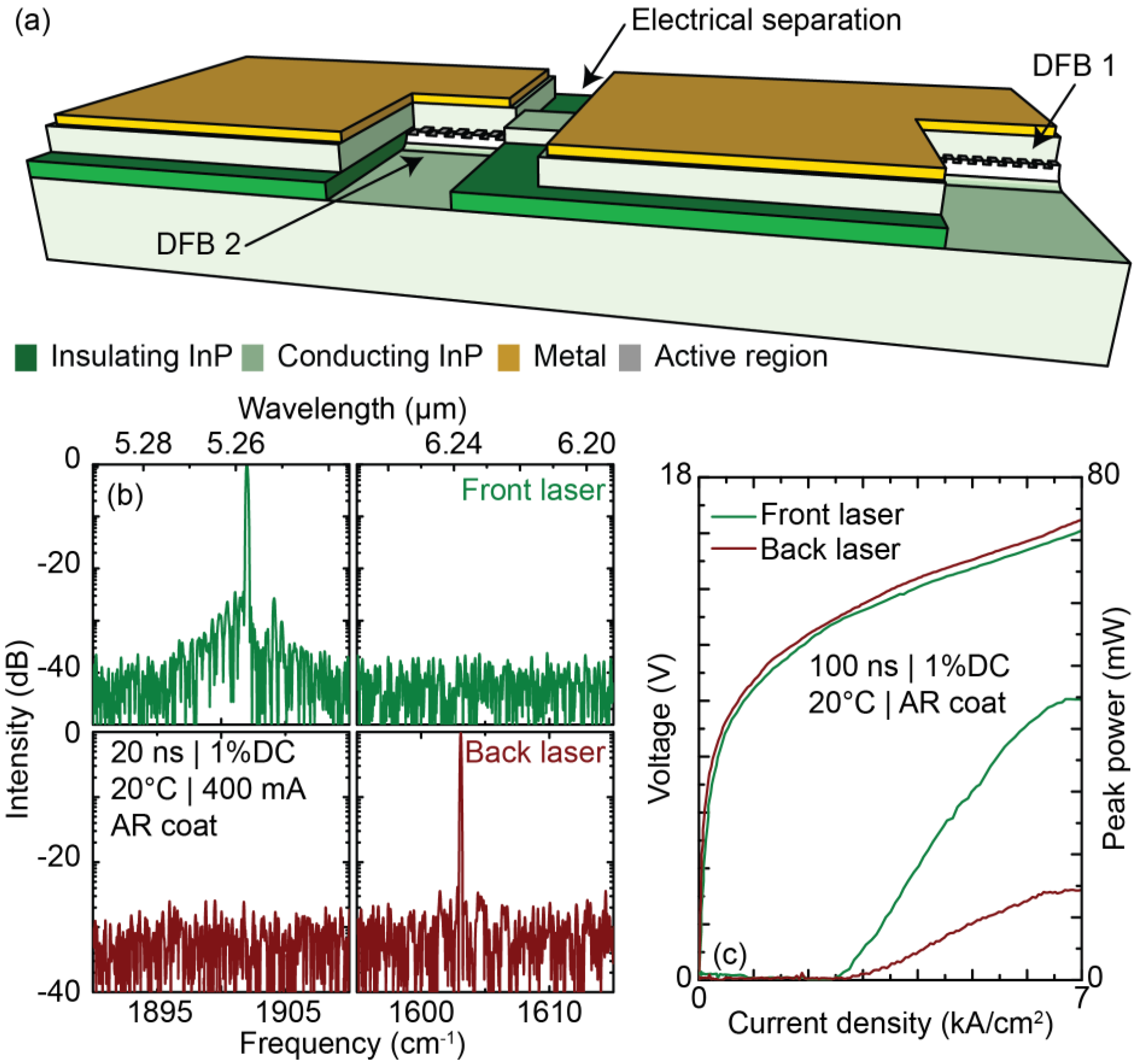
The devices consist of two sections, a front and a back section, with separate DFB gratings, corresponding to the desired wavelengths (
Figure 9a). The active core is a hetero-stack of two different quantum cascades with a gain profile optimized to cover the desired spectral regions. In
Figure 9b, a laser is shown that emits close to 1600 cm
−1 and 1900 cm
−1, in order to target two different nitrous oxide species, which have relevance for environmental gas monitoring. The two sections are electrically isolated in order to allow individual pumping and to minimize cross-talk. These lasers show threshold current density of 2.5 kA/cm
2 and up to 45 mW peak power in pulsed operation at room temperature, as demonstrated by light-current-voltage characteristics shown in
Figure 9c. Such lasers can simply replace single wavelength devices in existing spectroscopic setups without the need for additional optical elements. In fact, the use of such a laser, together with suitable driving electronics has led to successful demonstrations of a spectroscopic application [
53,
54].
8. Photonic Crystal QCLs
Some applications, such as open-path spectroscopy, benefit specifically from high-power single-mode operation with a proper beam shape [
55,
56]. Although DFB QCLs achieve high output power values, their maximum output power is limited due to the appearance of parasitic modes when increasing the length or width of the device. To achieve a high power output combined with high spectral purity, photonic crystal (PhC) lasers were proposed in the near-infrared [
57].
The PhC approach as a mode control strategy was also applied in QCLs. The first attempts featured photonic crystals with air holes and plasmonic waveguiding, which provided a strong index contrast for mode selection, but the resulting poor heat extraction and high modal losses at the metal-semiconductor interface prevented room temperature operation [
58]. Other approaches replaced one-dimensional DFB corrugations in the top cladding with a two-dimensional periodic structure, but despite the high optical power, the spectral purity was impaired by the low index contrast [
59]. In this work we combine a buried heterostructure fabrication process [
2,
34,
60] with a PhC deep-etched into the active region via inductively coupled plasma (ICP) etching, in order to combine the benefits of a strong material index contrast (~10%) and good heat extraction due to the monolithic contact between active region and regrown InP.
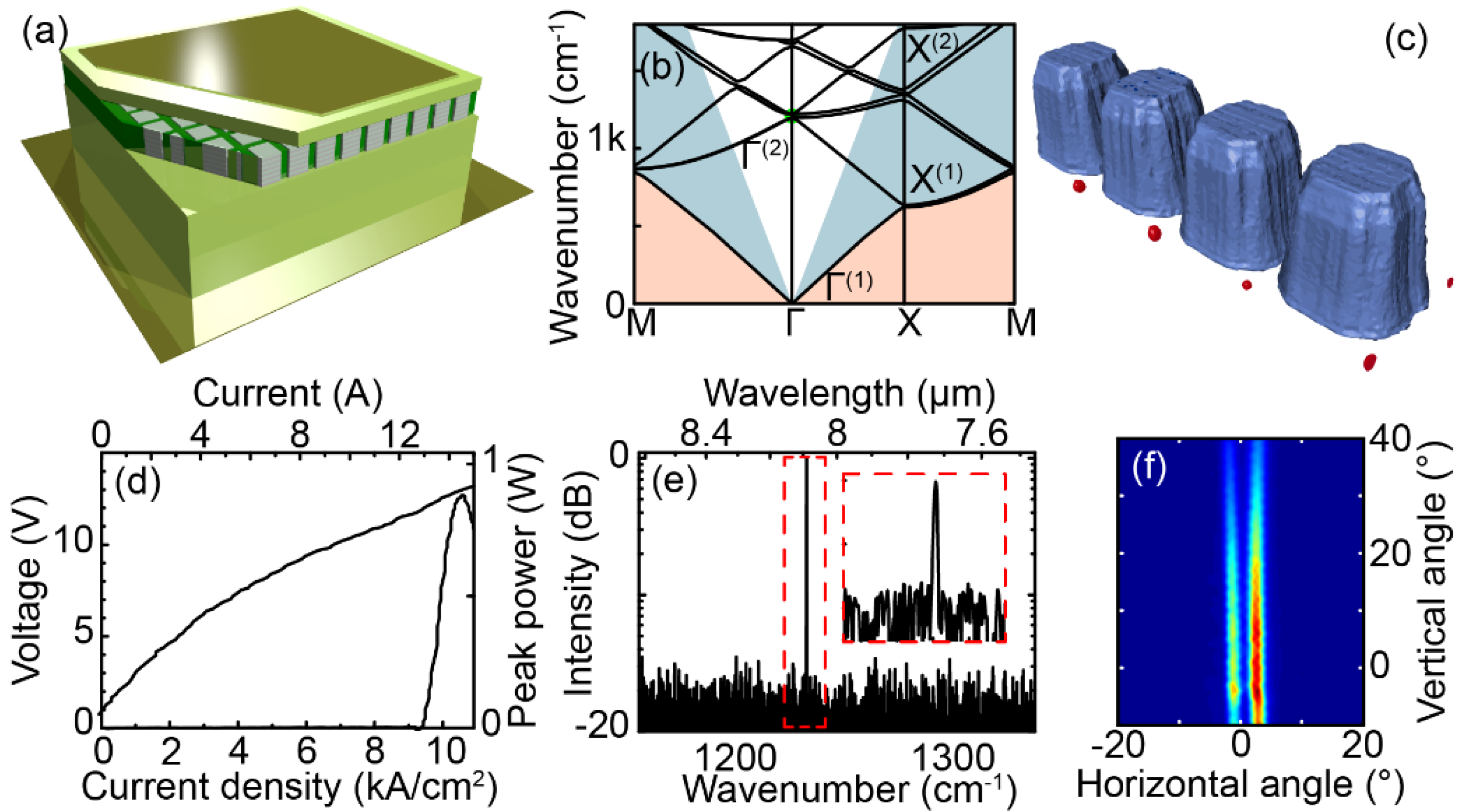
Finite difference time domain (FDTD) simulations of PhC (
Figure 10) yield photonic band diagram (
Figure 10b) and predict an effective refractive index contrast in this device geometry of about 7%, which is high enough to keep single mode operation over a large area (550 µm side square). Primary laser action is designed to occur in the Γ
(2) point (marked green in
Figure 10b) in order to keep a large enough period size for the fabrication process. The volume overlap factor of the mode in Γ
(2) with the active region is 0.44 enabling an efficient use of the gain.
For the fabrication of the buried-heterostructure PhC QCLs, we follow the same process protocol as for standard iBH lasers [
34]. However, in contrast, the lateral regrowth of the Fe-doped semi-insulating InP grown around the pillars is performed with HVPE (due to considerations discussed in
Section 3). The conductive InP cladding is grown with conventional MOVPE regrowth techniques.
To control the process we performed structural analysis through focused ion beam and scanning electron microscopy using slice and view strategy (
Figure 10c and
supplementary video), revealing the active region and the laterally regrown insulating InP. The small periodic voids appearing below the active region (
Figure 10c, red) are due to an ICP over-etching during the definition of the active region pillars via inductive coupled plasma reactive ion etching. The over-etched surface at the bottom prevents proper regrowth conditions and creates voids filled with the atmospheric components in the HVPE reactor. Although the regrowth quality is sufficient in quality close to the active region, the process can still be tailored to avoid such artifacts altogether, in order to further improve the mode selection and the thermal performance.
Typical experimental results of such devices show a threshold of 9.4 kA/cm
2 (
Figure 10d) and a single mode behavior (
Figure 10e). The threshold is twice as high as for separately processed Fabry-Perot reference devices from the same wafer, which is attributed to an incomplete Fe incorporation during the HPVE regrowth. The resulting lower barrier height in the isolating InP is responsible for leakage currents indicated in the shape of the IV characteristic. Despite all the process deficiencies, peak powers up to 0.88 W were recorded, which are approaching the best performing DFB devices [
21]. In far field experiments two lobes are observed (
Figure 10f). The recorded patterns are narrow in the horizontal direction, indicating that the lasing mode is a diffraction limited second order mode of the PhC mesa, and broad in the vertical direction conforming with diffraction through the height of the facet.
These results indicate that with further technological improvements (e.g., improvement of the PhC design, fully leveraging on the thermal dissipation through regrowth optimization) this approach can meet the requirements of photo acoustic spectroscopy, micro-surgery, or military countermeasures.
9. Conclusions
In this article we have summarized our latest achievements in the field of mid-infrared quantum cascade lasers. We have improved our active region growth by introducing material characterization protocols combining global and local techniques to assess crystallography, morphology, and chemistry. Advances in fabrication techniques, such as grating definition, waveguide etching, regrowth techniques, and optimization, as well as cladding engineering, have also helped to improve the device performances.
Our advances are demonstrated by well-functioning devices. We have demonstrated improved performances owing to a rigorous fabrication optimization in short-wavelength QCLs. The optimized devices are low dissipation emitters, single-mode, and operate in a continuous wave manner up to 15 °C. Our advances in QCL process techniques also made the fabrication of a fully buried PhC QCL operating at room temperature possible. We further designed QCL arrays that, due to their grating concepts, are immune to the phase relation between mode and facet and are, therefore, suitable for a precise mode control. The issue of spatial separation is overcome by an additional fabrication step, where a collector waveguide equipped with second order DFB gratings is monolithically bonded to the backside of the laser array. Other multi-wavelength QCLs, which leverage on two electrically separated DFB gratings have been fabricated. These devices are facet emitters able to emit two wavelengths independently and are suitable light sources for simultaneous trace gas analysis of two or more gases. There is still room for improvements in terms of performance in all presented devices, and our repertoire of material characterization techniques is very suitable to identify the process steps requiring an optimization.
Nowadays, the QCL is a mature device and is at the verge to be included in full systems or products. The works we presented here, besides the performances themselves, consist of the building of a tool box for MIR QCL technology in general. All these efforts will allow better and cheaper integration in existing system as well as bring new possibilities for extending the use of QCL for novel and even unforeseen applications. For instance QCL frequency comb spectroscopy is a contemporary application of utmost interest since it can reach high performance in terms of spectral coverage in small-footprint systems [
61,
62,
63]. All of the studies presented above will help to improve QCL frequency combs through an overall better fabrication, as well as to extend their use to other wavelength ranges or to allow spatial combination of combs.

 ,
, 


