A High-Temperature Solar Selective Absorber Based upon Periodic Shallow Microstructures Coated by Multi-Layers Using Atomic Layer Deposition

Abstract
: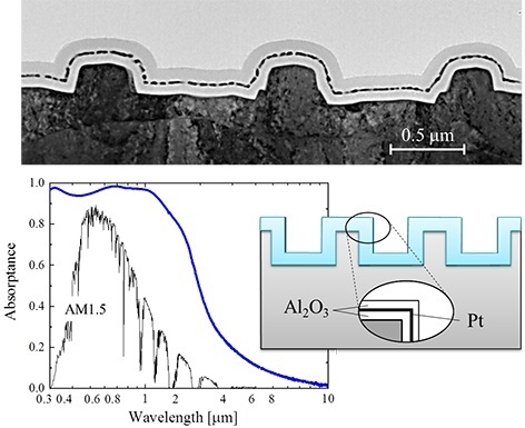
1. Introduction
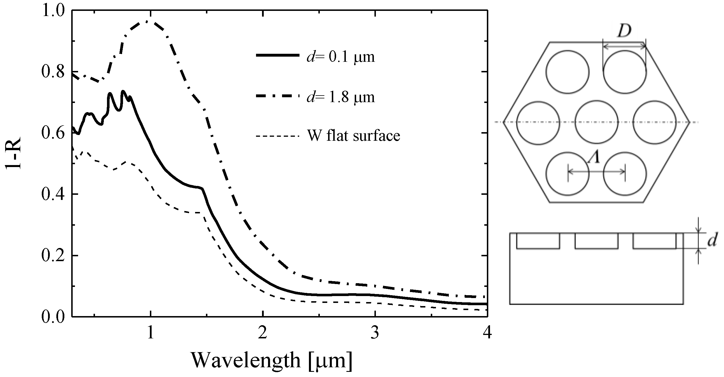
2. Honeycomb Array Cylindrical Microcavity Structure
2.1. Optical Simulation Based on Rigorous Coupled-Wave Analysis
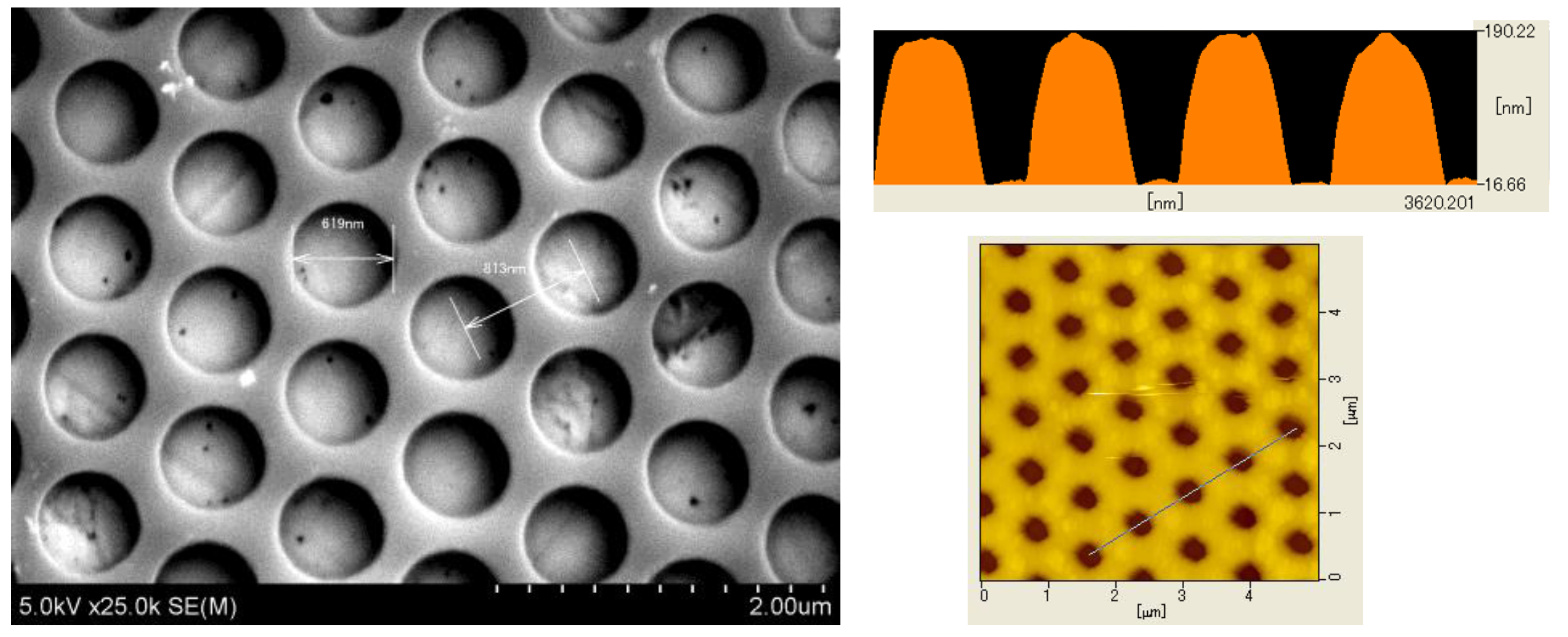
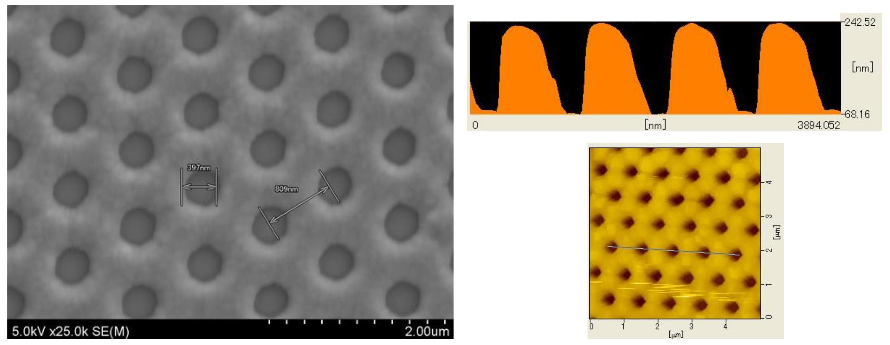
2.2. Fabrication of Honeycomb Array Shallow Cylindrical Microcavity
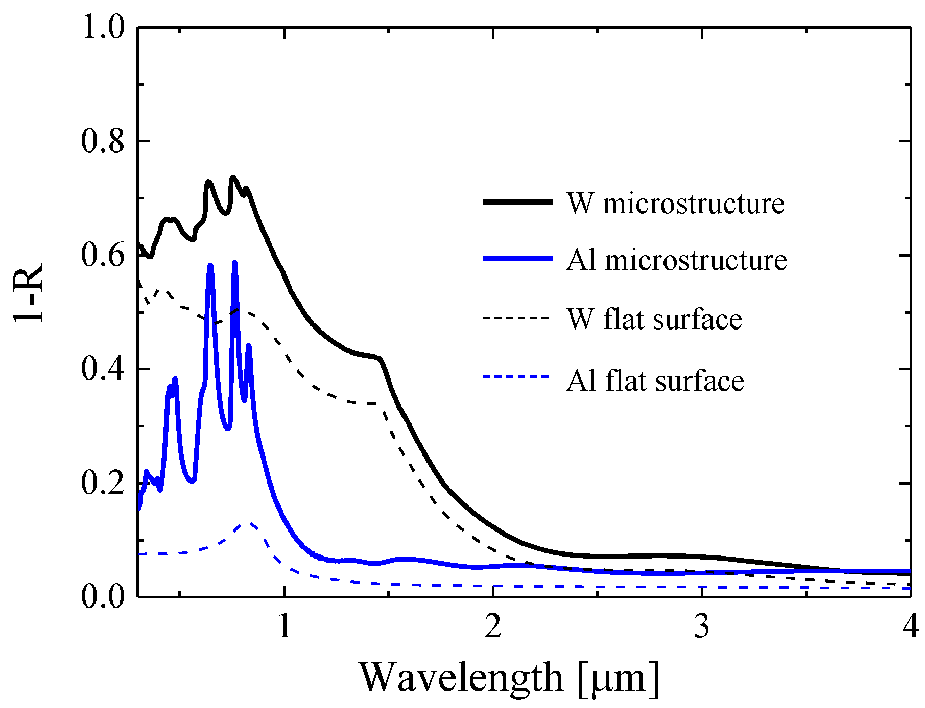
3. Honeycomb Array Cylindrical Microcavity with Multilayer Coating
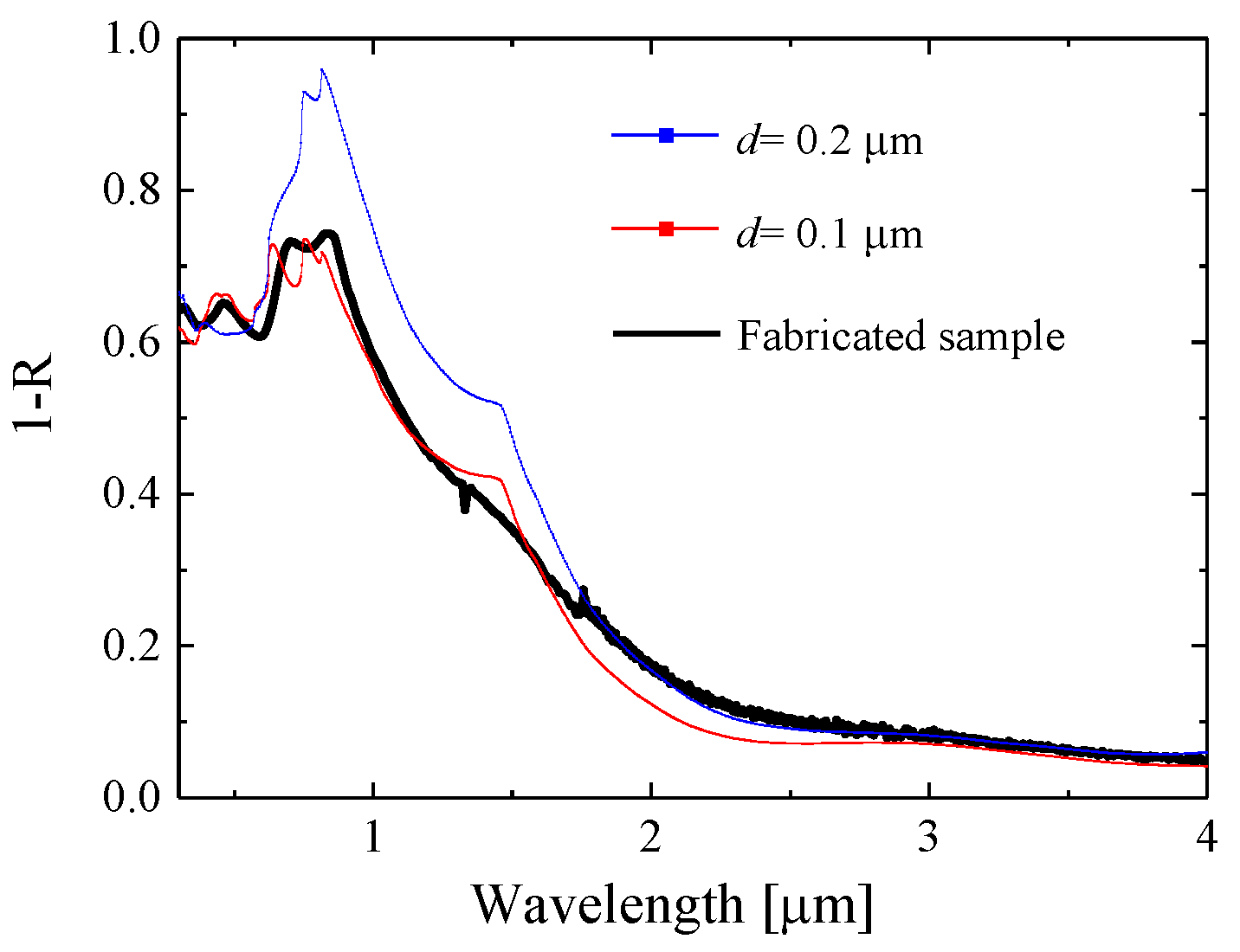
3.1. Numerical Simulation
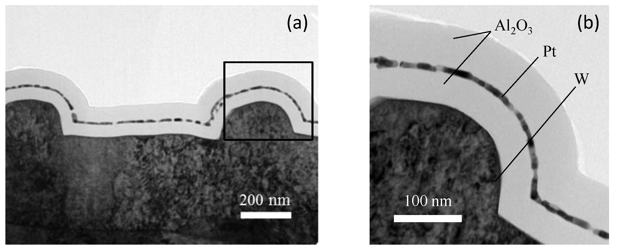
3.2. Fabrication of Honeycomb Array Cylindrical Microcavity with Multilayer Coating
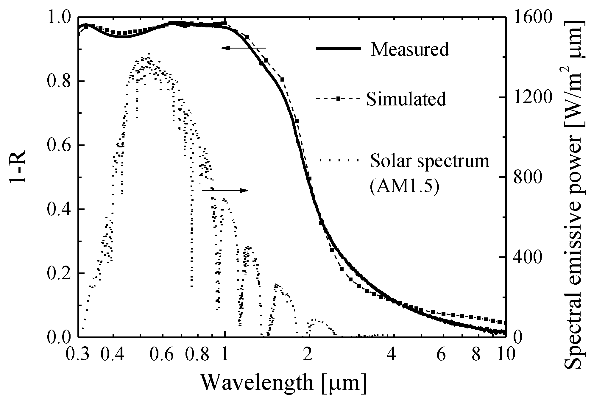
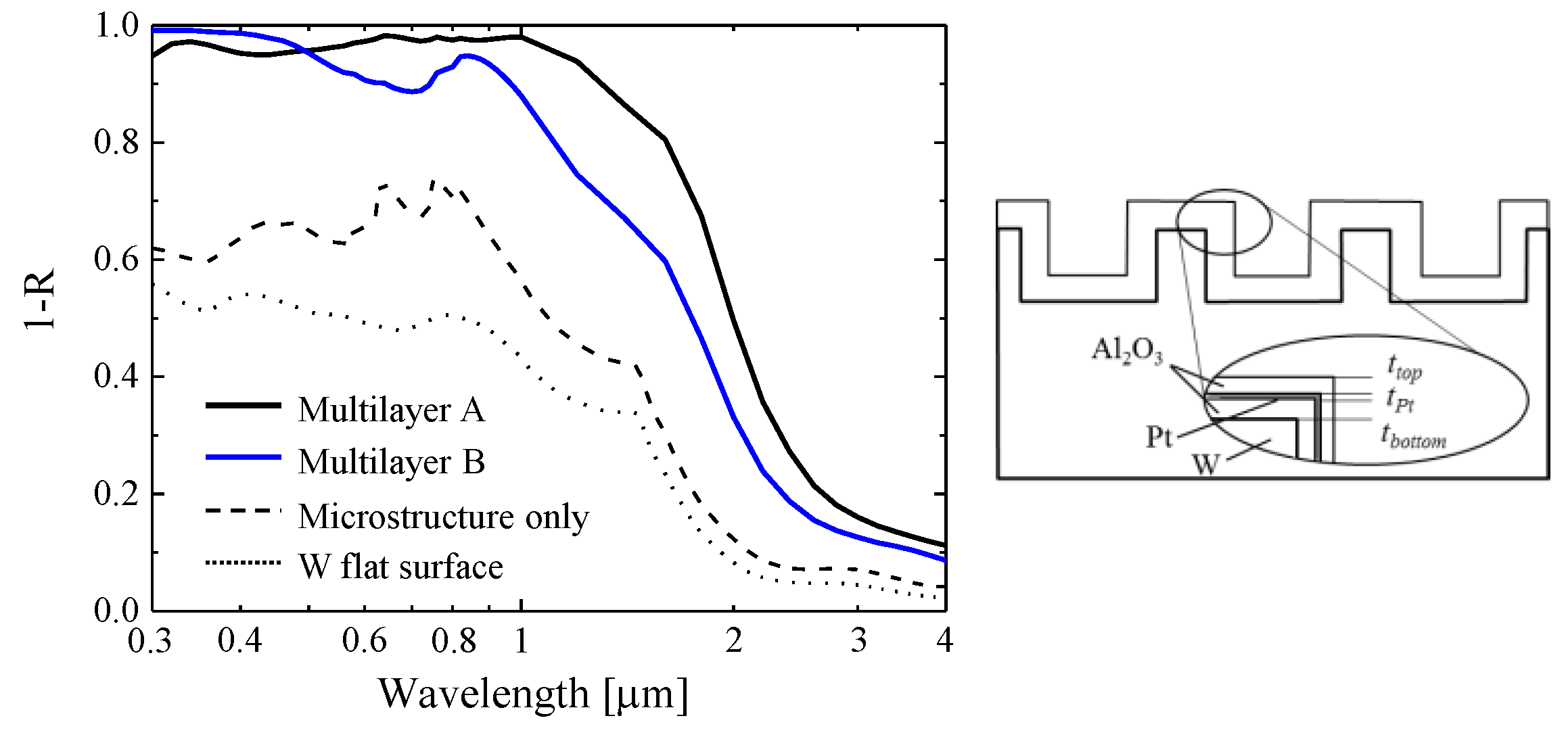
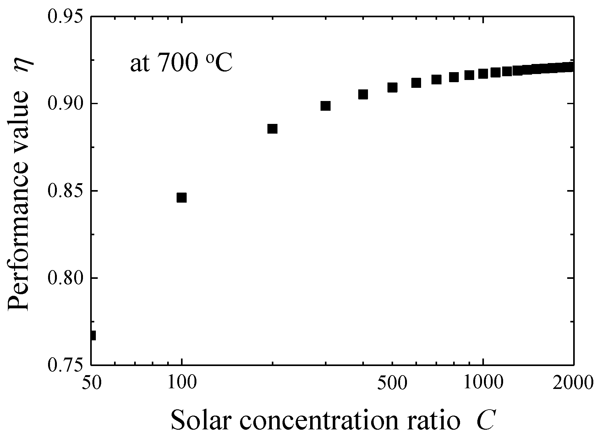
3.3. Evaluation of the Performance
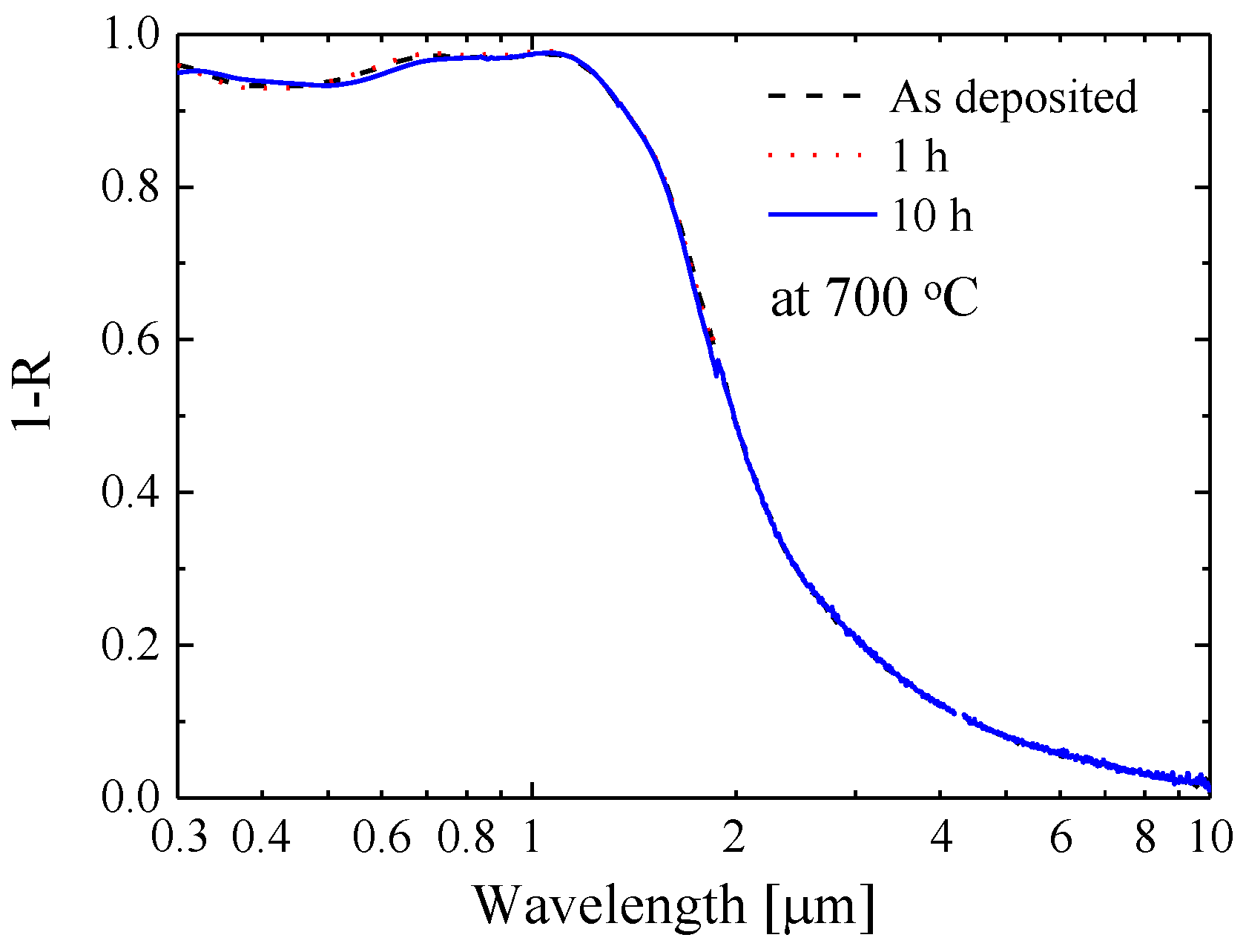
3.4. Thermal Stability Test
4. Conclusions
Acknowledgments
Author Contributions
Conflicts of Interest
References
- Giostri, A.; Binotti, M.; Astolfi, M.; Silva, P.; Macchi, E.; Manzolini, G. Comparison of different solar plants based on parabolic trough technology. Sol. Energy 2012, 86, 1208–1221. [Google Scholar] [CrossRef]
- Pavlović, T.M.; Radonjić, I.S.; Milosavljević, D.D.; Pantić, L.S. A review of concentrating solar power plants in the world and their potential use in Serbia. Renew. Sustain. Energy Rev. 2012, 16, 3891–3902. [Google Scholar] [CrossRef]
- Tian, Y.; Zhao, C.Y. A review of solar collectors and thermal energy storage in solar thermal applications. Appl. Energy 2013, 104, 538–553. [Google Scholar] [CrossRef] [Green Version]
- Maccari, A.; Bissi, D.; Casubolo, G.; Guerrini, F.; Lucatello, L.; Luna, G.; Zuanella, M. Archimede Solar Energy Molten Salt Parabolic Trough Demo Plant: A Step Ahead towards the New Frontiers of CSP. Energy Procedia 2015, 69, 1643–1651. [Google Scholar] [CrossRef]
- Tanaka, Y.; Tarutani, Y.; Magoshi, R.; Nakano, T. Feature and Operating Experience of 1000 MW Class Steam Turbine with Highest Efficiency in the World. Mitsubishi Juko Giho 2002, 39, 132–135. [Google Scholar]
- Agüero, A.; Muelas, R.; Pastor, A.; Osgerby, S. Long exposure steam oxidation testing and mechanical properties of slurry aluminide coatings for steam turbine components. Surf. Coat. Technol. 2005, 200, 1219–1224. [Google Scholar] [CrossRef]
- Gubbels, G.H.M.; Wolff, L.R.; Metselaar, R. A thermionic energy converter with a molybdenum-alumina cermet emitter. J. Appl. Phys. 1990, 68, 5856–5865. [Google Scholar] [CrossRef]
- Zhang, Q.C.; Yin, Y.B.; Mills, D.R. High efficiency Mo-Al2O3 cermet selective surfaces for high-temperature application. Sol. Energy Mater. Sol. Cells 1996, 40, 43–53. [Google Scholar] [CrossRef]
- Zhang, Q.C. Stainless-steel-AlN cermet selective surfaces deposited by direct current magnetron sputtering technology. Sol. Energy Mater. Sol. Cells 1998, 52, 95–106. [Google Scholar] [CrossRef]
- Barshilia, H.C.; Selvakumar, N.; Vignesh, G.; Rajam, K.S.; Biswas, A. Optical properties and thermal stability of pulsed-sputter-deposited AlxOy/Al/AlxOy multilayer absorber coatings. Sol. Energy Mater. Sol. Cells 2009, 93, 315–323. [Google Scholar] [CrossRef]
- Selvakumar, N.; Barshilia, H.C.; Rajam, K.S.; Biswas, A. Structure, optical properties and thermal stability of pulsed sputter deposited high temperature HfOx/Mo/HfO2 solar selective absorbers. Sol. Energy Mater. Sol. Cells 2010, 94, 1412–1420. [Google Scholar] [CrossRef]
- Chester, D.; Bermel, P.; Joannopoulos, J.D.; Soljacic, M.; Celanovic, I. Design and global optimization of high-efficiency solar thermal systems with tungsten cermets. Opt. Express 2011, 19, A245–A257. [Google Scholar] [CrossRef] [PubMed]
- Selvakumar, N.; Manikandanath, N.T.; Biswas, A.; Barshilia, H.C. Design and fabrication of highly thermally stable HfMoN/HfON/Al2O3 tandem absorber for solar thermal power generation applications. Sol. Energy Mater. Sol. Cells 2012, 102, 86–92. [Google Scholar] [CrossRef]
- Maruyama, S.; Kashiwa, T.; Yugami, H.; Esashi, M. Thermal radiation from two-dimensionally confined modes in microcavities. Appl. Phys. Lett. 2001, 79, 1393–1395. [Google Scholar] [CrossRef]
- Sai, H.; Kanamori, Y.; Yugami, H. High-temperature resistive surface grating for spectral control of thermal radiation. Appl. Phys. Lett. 2003, 82, 1685–1687. [Google Scholar] [CrossRef]
- Sai, H.; Yugami, H.; Kanamori, Y.; Hane, K. Solar selective absorbers based on two-dimensional W surface gratings with submicron periods for high-temperature photothermal conversion. Sol. Energy Mater. Sol. Cells 2003, 79, 35–49. [Google Scholar] [CrossRef]
- Rinnerbauer, V.; Yeng, Y.X.; Chan, W.R.; Senkevich, J.J.; Joannopoulos, J.D.; Soljačić, M.; Celanovic, I. High-temperature stability and selective thermal emission of polycrystalline tantalum photonic crystals. Opt. Express 2013, 21, 11482–11491. [Google Scholar] [CrossRef] [PubMed]
- Wang, H.; Wang, L. Perfect selective metamaterial solar absorbers. Opt. Express 2013, 21, A1078–A1093. [Google Scholar] [CrossRef] [PubMed]
- Shemelya, C.; DeMeo, D.; Latham, N.P.; Wu, X.; Bingham, C.; Padilla, W.; Vandervelde, T.E. Stable high temperature metamaterial emitters for thermophotovoltaic applications. Appl. Phys. Lett. 2014, 104, 201113. [Google Scholar] [CrossRef]
- Moharam, M.G.; Gaylord, T.K. Rigorous coupled-wave analysis of planar-grating diffraction. J. Opt. Soc. Am. B Opt. Phys. 1981, 71, 811–818. [Google Scholar] [CrossRef]
- Ghebrebrhan, M.; Bermel, P.; Yeng, Y.X.; Celanovic, I.; Soljačić, M.; Joannopoulos, J.D. Tailoring thermal emission viaQmatching of photonic crystal resonances. Phys. Rev. B Condens. Matter. 2011, 83, 033810. [Google Scholar] [CrossRef]
- Sai, H.; Kanamori, Y.; Yugami, H. Tuning of the thermal radiation spectrum in the near-infrared region by metallic surface microstructures. J. Micromech. Microeng. 2005, 15, S243–S249. [Google Scholar] [CrossRef]
- Savas, T.A.; Schattenburg, M.L.; Carter, J.M.; Smith, H.I. Large-area achromatic interferometric lithography for 100 nm period gratings and grids. J. Vac. Sci. Technol. B 1996, 14, 4167–4170. [Google Scholar] [CrossRef]
- Chen, C.G.; Konkola, P.T.; Heilmann, R.K.; Joo, C.; Schattenburg, M.L. Nanometer-accurate grating fabrication with scanning beam interference lithography. In Proceedings of the SPIE’s International Symposium on Smart Materials, Nano-, and Micro-Smart Systems, Melbourne, Australia, 16 December 2002; Volume 4936, pp. 126–134.
- Si, G.; Wang, Q.; Lv, J.; Miao, L.; Wang, F.; Peng, S. Interference lithography patterned large area plasmonic nanodisks for infrared detection. Mater. Lett. 2014, 128, 373–375. [Google Scholar] [CrossRef]
- De Boor, J.; Geyer, N.; Gösele, U.; Schmidt, V. Three-beam interference lithography: Upgrading a Lloyd’s interferometer for single-exposure hexagonal patterning. Opt. Lett. 2009, 34, 1783–1785. [Google Scholar] [CrossRef] [PubMed]
- Shimizu, M.; Yamada, T.; Sasaki, K.; Takada, A.; Nomura, H.; Iguchi, F.; Yugami, H. Anisotropic multi-step etching for large-area fabrication of surface microstructures on stainless steel to control thermal radiation. Sci. Technol. Adv. Mater. 2016, 16, 025001. [Google Scholar] [CrossRef]
- Hall, A.C.; Ambrosini, A.; Ho, C.K.; McCloskey, J.F.; van Every, K.; McCloskey, J.F.; Urrea, D.A.; Lambert, T.N.; Bencomo, M.; Mahoney, A.R.; et al. Solar Selective Coatings for Concentrating Solar Power Central Receivers. Adv. Mater. Process. 2012, 170, 28–32. [Google Scholar]
- Shimizu, M.; Kohiyama, A.; Yugami, H. High-efficiency solar-thermophotovoltaic system equipped with a monolithic planar selective absorber/emitter. J. Photonics Energy 2015, 5, 053099. [Google Scholar] [CrossRef]
- Aaltonen, T.; Ritala, M.; Sajavaara, T.; Keinonen, J.; Leskelä, M. Atomic layer deposition of platinum thin films. Chem. Mater. 2003, 15, 1924–1928. [Google Scholar] [CrossRef]
- Aaltonen, T.; Ritala, M.; Tung, Y.L.; Chi, Y.; Arstila, K.; Meinander, K.; Leskelä, M. Atomic layer deposition of noble metals: Exploration of the low limit of the deposition temperature. J. Mater. Res. 2004, 19, 3353–3358. [Google Scholar] [CrossRef]
- Juppo, M.; Rahtu, A.; Ritala, M.; Leskelä, M. In situ mass spectrometry study on surface reactions in atomic layer deposition of Al2O3 thin films from trimethylaluminum and water. Langmuir 2000, 16, 4034–4039. [Google Scholar] [CrossRef]
- Elam, J.W.; Routkevitch, D.; Mardilovich, P.P.; George, S.M. Conformal coating on ultrahigh-aspect-ratio nanopores of anodic alumina by atomic layer deposition. Chem. Mater. 2003, 15, 3507–3517. [Google Scholar] [CrossRef]
- Shrestha, P.; Gu, D.; Tran, N.; Tapily, K.; Baumgart, H.; Namkoong, G. Investigation of Volmer-Weber Growth during the Nucleation Phase of ALD Platinum Thin Films and Template Based Platinum Nanotubes. ECS Trans. 2010, 33, 127–134. [Google Scholar]


© 2016 by the authors; licensee MDPI, Basel, Switzerland. This article is an open access article distributed under the terms and conditions of the Creative Commons by Attribution (CC-BY) license (http://creativecommons.org/licenses/by/4.0/).
Share and Cite
Shimizu, M.; Akutsu, H.; Tsuda, S.; Iguchi, F.; Yugami, H. A High-Temperature Solar Selective Absorber Based upon Periodic Shallow Microstructures Coated by Multi-Layers Using Atomic Layer Deposition. Photonics 2016, 3, 13. https://doi.org/10.3390/photonics3020013
Shimizu M, Akutsu H, Tsuda S, Iguchi F, Yugami H. A High-Temperature Solar Selective Absorber Based upon Periodic Shallow Microstructures Coated by Multi-Layers Using Atomic Layer Deposition. Photonics. 2016; 3(2):13. https://doi.org/10.3390/photonics3020013
Chicago/Turabian StyleShimizu, Makoto, Hiroki Akutsu, Shinichiro Tsuda, Fumitada Iguchi, and Hiroo Yugami. 2016. "A High-Temperature Solar Selective Absorber Based upon Periodic Shallow Microstructures Coated by Multi-Layers Using Atomic Layer Deposition" Photonics 3, no. 2: 13. https://doi.org/10.3390/photonics3020013