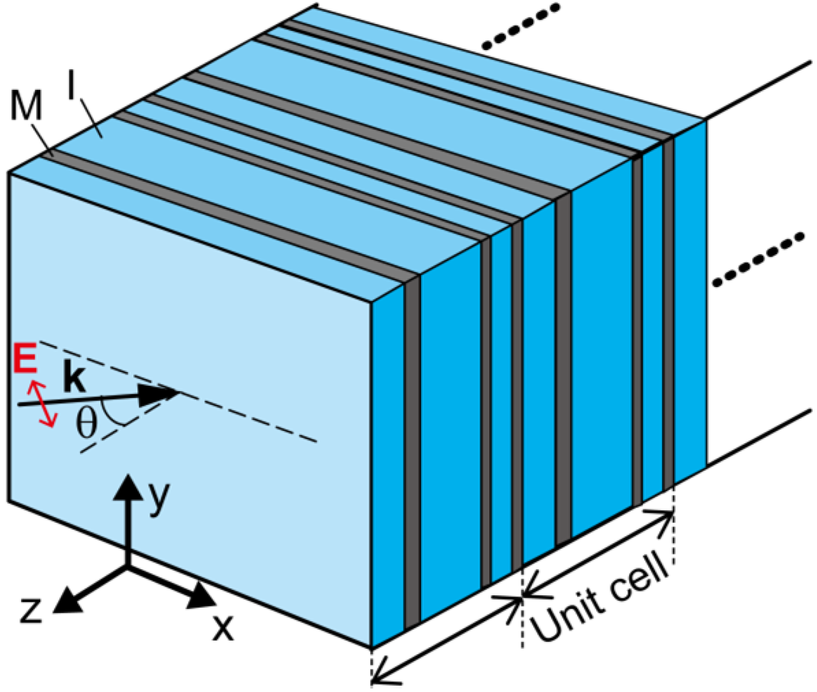
Figure 1 depicts a schematic of the SMIM of a complex unit cell; a SMIM of a six-layer unit cell is illustrated to show the incident configuration. The coordinate system is defined such that the
plane is parallel to the metal (M) and insulator (I) layers, which are shown with gray and pale blue, respectively, and the
z axis is parallel to the stacked direction. The M and I layers are assumed to spread enough along the
plane. The plane of incidence is set to be parallel to the
plane; the
p-polarized incident plane wave is shown, and then the electric-field (E-field) vector
is parallel to the
plane. When incident light is
s polarized, the E-field vector satisfies with
.
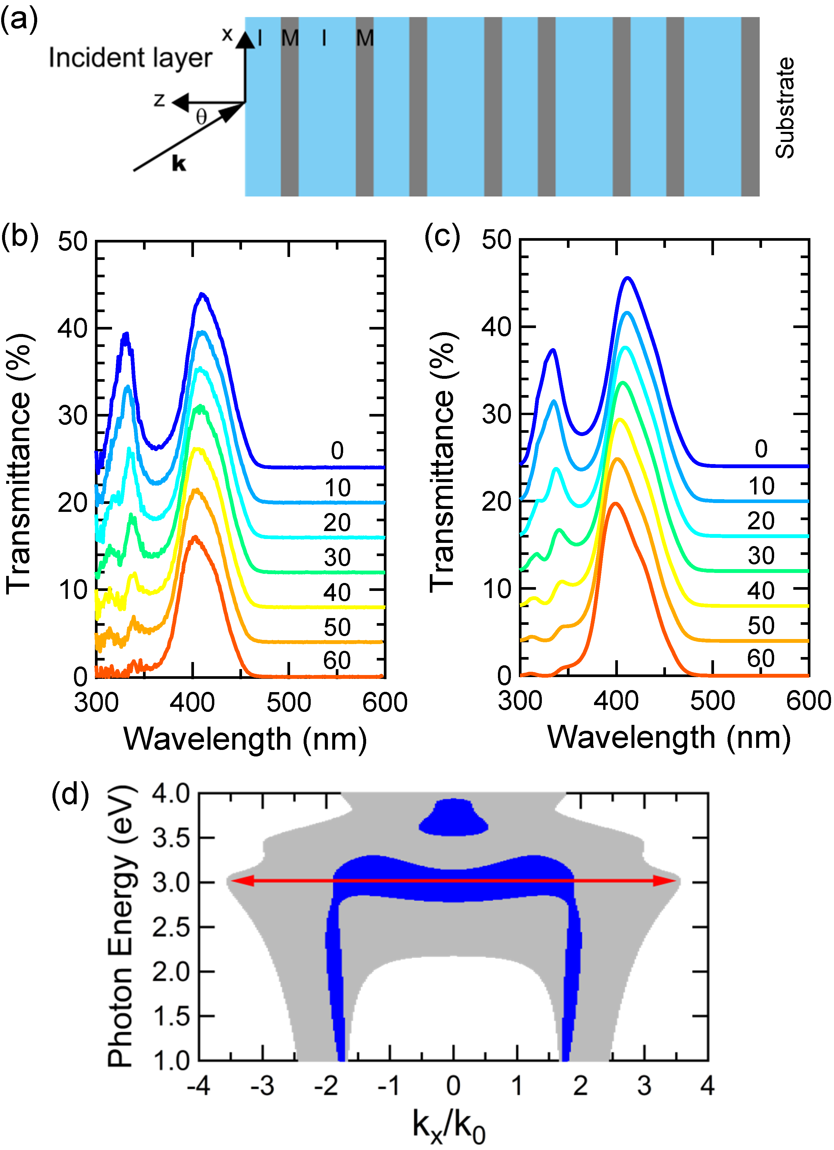
2.1. Four-Layer Unit Cell for Blue Wavelengths
Figure 2a shows a schematic illustration of a SMIM of a four-layer unit cell of (SiO
50 nm/Ag 25 nm/SiO
80 nm/Ag 25 nm). A SiO
layer of 50 nm in thickness is exposed to the incident layer of air. The SMIM comprises 16 layers in total and has a 720-nm thickness. A feature of the SMIM is the transmission window at 410 nm.
Measured and calculated T spectra under
p polarization are shown in
Figure 2b and c, respectively. The T spectra are shown with an offset for clarity, represented in the top-to-bottom manner in accordance with incident angles 0
to 60
. The measured T spectra show a quantitatively good agreement with the calculated ones for the wide incident angles. The specimen was made by ion-beam sputtering onto a SiO
substrate; the thin-film growth enabled highly precise control of the thickness of each layer. The numerical calculation was implemented by using the scattering-matrix (S-matrix) algorithm [
26] and by taking the measured permittivity of Ag [
27] and the typical permittivity of SiO
, 2.1316, and air, 1.00054.
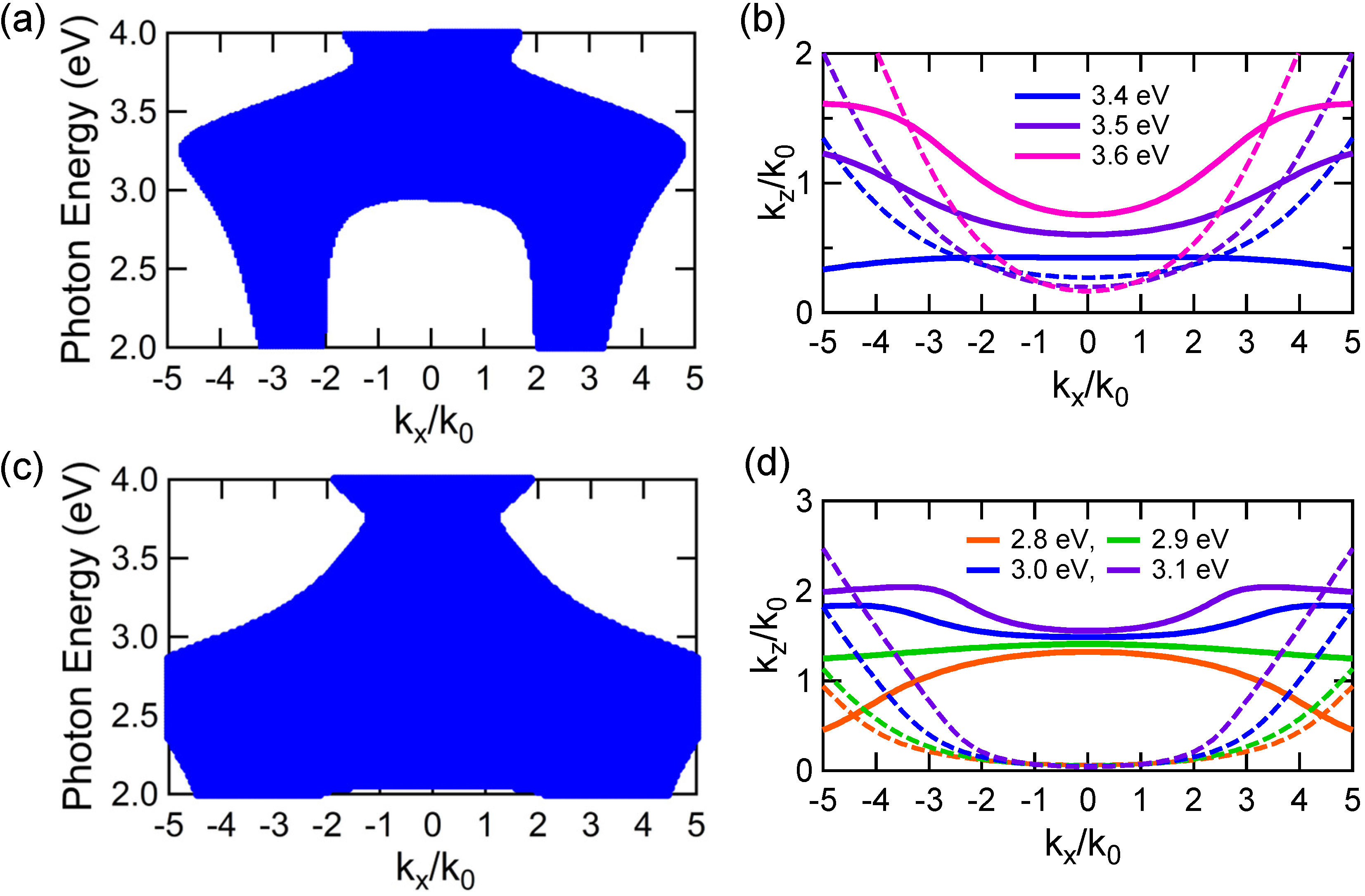
Figure 2d presents the transmission Bloch band of the SMIM of the four-layer unit cell at transverse magnetic (TM) polarization, at which we set the E-field vector to be in the
plane. We mention that the TM polarization corresponds to
p polarization in the illuminating configuration of
Figure 1. The Bloch band is well defined in perfectly periodic SMIMs, which was determined by solving the following eigenvalue equation:
where
denotes the
transfer matrix for one periodicity
d,
is the EM-field component propagating for
directions, respectively, and
is an arbitrary
z value [
22]. The derivation of the transfer matrix was straightforward, composed of the product of interface and boost matrices, and was explicitly shown in [
19,
21]. Note that the transfer matrix
depends only on
. Bloch states in SMIMs are indexed with
K in Equation (1), which determines the propagation characteristics for the
z axis; the explicit form is given by:
where
m is an integer and gives a branch only to the real part of the
K. Thus, there remains the problem to determine a proper branch, which is examined later. Note that the Bloch band is independent of the value of
. At TM polarization,
F is the
y component of the magnetic field, whereas, at TE (transverse electric) polarization (
),
F is the
y component of the E-field. The transmission Bloch bands (blue and thin gray) in
Figure 2d were obtained under the exponentially non-growing condition for
, such as
and
, respectively; we call the former low-loss condition and the latter relatively large loss. Strictly, the Bloch bands in realistic SMIMs are quasi-transmission bands because optical loss is inevitable. This point is different from the Bloch bands in loss-free dielectric multilayer structures [
18].
In
Figure 2d, a feature in the Bloch band appears, for which the
component widely supports the transmission Bloch band at about 3.0 eV (double-ended arrow). The wide
mode was recently employed to realize SR imaging with sub-50-nm resolution by implementing a hyperlens in an optical microscope [
9]. It is also to be noted that a small
band shown with blue manifests itself as T peaks in
Figure 2b,c. Thus, the Bloch state is well supported by the experimental data.
Figure 2.
(a) Schematic of a SMIM of the four-layer unit cell, which has a transmission window at 410 nm. (b,c) Measured and computed T spectra under p polarization, respectively, which are shown with an offset for clarity. The incident angle varied from to at steps. (d) Transmission Bloch band at transverse magnetic (TM) polarization. Blue and light gray correspond to the low-loss and relatively large-loss bands described in the text, respectively. Double-ended arrows indicate the peak of transmission at 3.02 eV (or 410 nm).
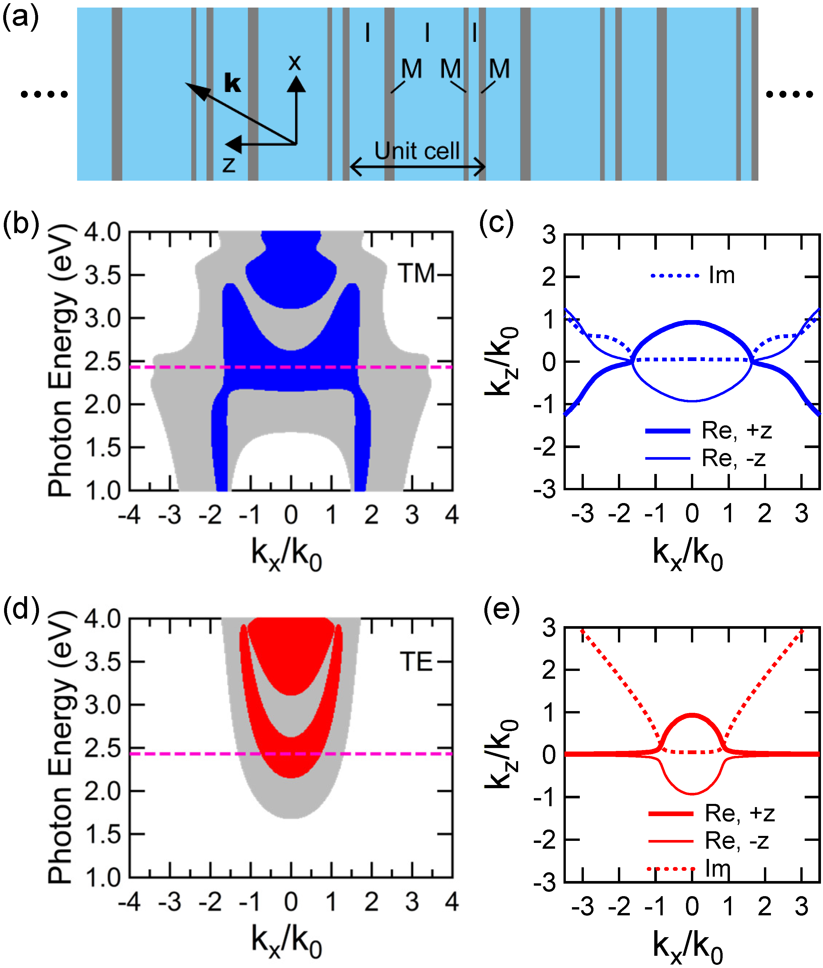
2.2. Six-Layer Unit Cell for Green Wavelengths
Figure 3a schematically draws a SMIM of the six-layer unit cell of (SiO
51.2 nm/Ag 14.7 nm/SiO
101.8 nm/Ag 7.4 nm/SiO
15.4 nm/Ag 9.5 nm). If the SMIM is a finite stacking, a SiO
layer of 51.2 nm in thickness is set to touch the incident layer of air and a Ag layer of 9.5 nm to touch the SiO
substrate. The unit cell was found through automatic search on a computer; the search started with the random generation of 30,000 unit cells of given periodicity and numbers of layers, selecting unit cells satisfying high T at 500 nm as independent as possible of the incident angles between 0
and 80
under
p polarization and then optimizing the best unit cell in the random generation. This automatic search is equivalent to a genetic algorithm search in the first generation; similar implementations to take optical quantity in MMs as the fitness were reported [
28,
29,
30]. In the present search, fitness in the genetic algorithm was the sum of T evaluated at 10
-step incident angles from 0
to 80
, and the constraint was the total thickness of the unit cell (200 nm) and the minimum thickness of each layer (5 nm). Finite SMIMs, which were composed of four unit cells, were searched. The SMIM of the best unit cell exhibits T more than 30% at 500 nm and
, even when it contains 24 layers, half of which are metallic layers. We mention that the best-designed SMIM requires highly precise control of each layer; in practice, the ion-beam sputtering that we employed in
Figure 2b is able to meet this precision. This is because, although the growth rates of Ag and SiO
were 0.31±0.03 and 0.17±0.03 nm/s, respectively, the temporal control less than 0.3 s makes it practically possible to realize 0.1-nm precision. Note again that the very good agreement of the experiment and theory in
Figure 2 was obtained by the sputtering method and would not be obtained by other film-making methods.
Figure 3b shows the transmission Bloch band of the SMIM of the six-layer unit cell at TM polarization, represented in a similar manner to
Figure 2d.
Figure 3c shows the equi-frequency TM-polarized contour at 2.4304 eV (or 510.0 nm in wavelength); the real part of
is shown with solid curves and the imaginary part with the dotted line. The real parts always contain both
- and
-propagation components, shown with bold and thin curves, respectively. The equi-frequency contour is peculiar to TM polarization; at the low-loss range (
), the Re(
) takes positive values and forms a convex shape for the
-propagation. At the other
range (
), the Re(
) becomes negative. The
contour is far from the so-called hyperbolic shape; nevertheless, the mode serves as a hyper mode, as shown later. Note that the imaginary part is shown only for the
-propagation component for simplicity.
Figure 3d shows the transmission Bloch band at TE polarization; red and light gray correspond to low-loss and relatively large-loss bands, respectively.
Figure 3e shows the equi-frequency TE-polarized contour at 510.0 nm; the real part of
is shown with solid curves and the imaginary part with the dotted line. The real parts associated with
- and
-propagation components are shown in a similar way to
Figure 2c. The imaginary part is also shown similarly to
Figure 2c. The equi-frequency contour is roughly spherical in shape around the origin, close to typical equi-frequency contours in insulators at non-resonant wavelengths.
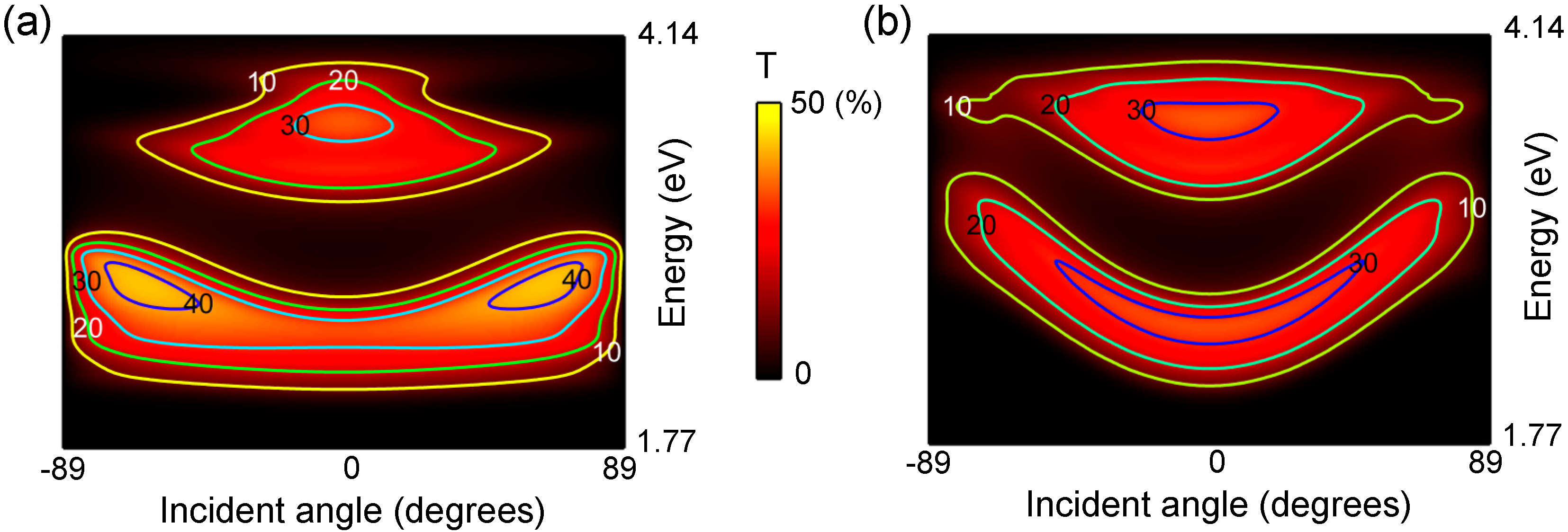
Figure 4 shows the T spectra of the SMIM of the six-layer unit cell (
Figure 3) in pseudo-color representation: (a) and (b) show TM and TE polarizations, respectively. To evaluate finite T, we set the SMIM to be 24-layers in total stacked on a SiO
substrate. In this case, the SMIM had an 800-nm thickness in total. A SiO
layer of 51.2 nm in thickness was set to touch the incident layer of air. Incident angles varied from
to
and, therefore, covered the
range of
in
Figure 3b,d. Evidently, the T peaks in
Figure 4 agree with the low-loss Bloch band in
Figure 3. Thus, the Bloch band is explicitly confirmed by the T spectra.
Figure 3.
(
a) Schematic of a SMIM of the six-layer unit cell that has a transmission window at 500 nm. The structural parameters are described in the text. (
b) Transverse magnetic (TM)-polarization Bloch band, shown in a similar manner to
Figure 2d. (
c) Equi-frequency TM contour at 2.4304 eV (or 510.0 nm). Solid lines denote the real part of
, and the dotted line the imaginary part. (
d) TE-polarization Bloch band; red denotes the low-loss band and light gray the relatively large-loss band. (
e) Equi-frequency TE contour at 510.0 nm, represented similarly to (c).
As was referred to in Equation (2), it is necessary to determine a proper branch of Bloch-state index
K, which is
in
Figure 3c,e. A direct way to determine the physical branch is shown in
Figure 5.
Figure 4.
(a,b) 2D plots of T at TM and TE polarizations, respectively, represented with pseudo-color and contours.
Figure 4.
(a,b) 2D plots of T at TM and TE polarizations, respectively, represented with pseudo-color and contours.
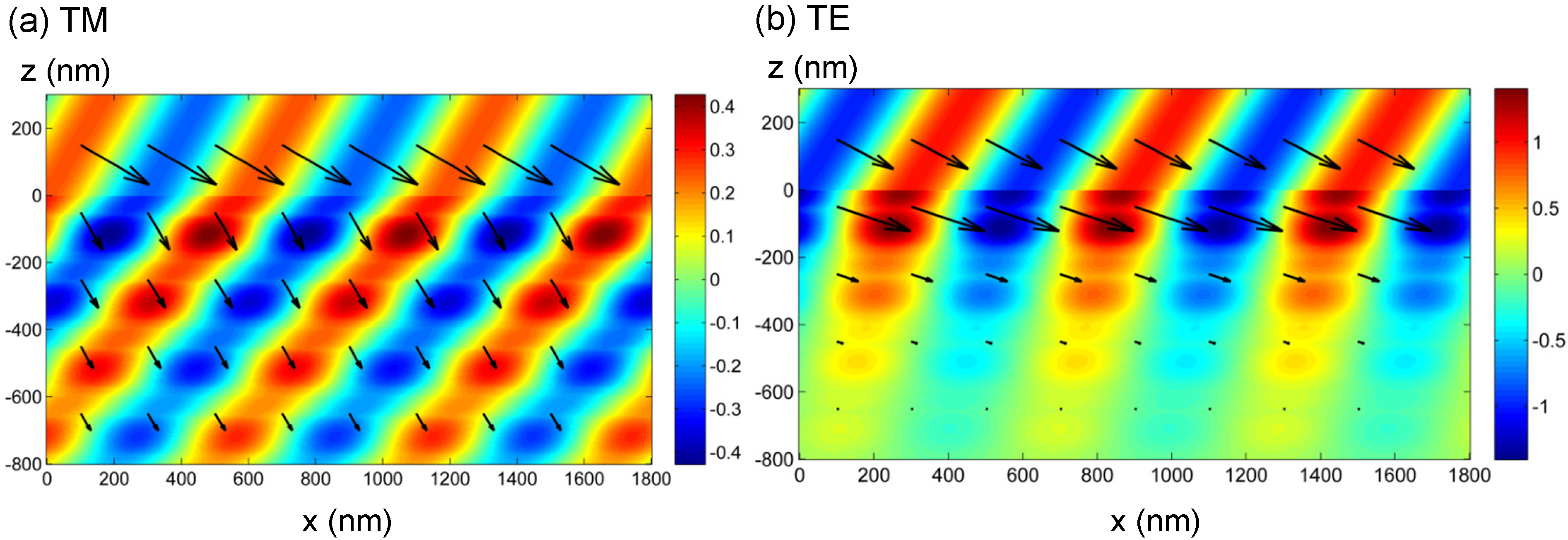
Figure 5.
Illumination of the SMIM of the six-layer unit cell. (a,b) Electromagnetic (EM)-field distributions (color plots) at TM and TE polarizations, respectively. Specifically, the color plots represent snapshots of (a) and (b) components. The incident wavelength was 510.0 nm, and the incident angle was set to 60. Arrows denote Poynting vectors in the plane.
Figure 5 shows EM-field distributions (color) and the Poynting vector (arrows) on the
plane at oblique incidence of
in the illumination configuration of
Figure 1. The color plots represent snapshots of
and
components in
Figure 5a,b, respectively. Incident light of 510.0 nm in wavelength travels from the top and sheds on the surface of the SMIM of the six-layer unit cell at
nm.
Figure 5a,b corresponds to TM and TE polarizations, respectively, and accordingly display the
and
components. Note that, in the incident layer, we plotted only the incident component to clearly visualize the oblique incidence, omitting the reflection component. A proper branch in Equation (2) was determined as follows. The incident angle of
means that the
holds the relation of
, where
is the
x component of wavevector in the SMIM and
wavenumber of light in air. The wave front is formed in the SMIM, and refraction is observed, suggesting that refraction angle
α at TM polarization is smaller than incident angle
θ and refraction angle
β at TE polarization larger than
θ; thus we have a relation of
, which implies that the
at TM polarization is larger than the
at TE polarization. Strictly, the E-field component in SMIMs contains both forward and backward components; therefore, the wave front does not necessarily provide a well-defined refraction angle. Still, in this case, the Poynting vector
in
Figure 4 is qualitatively consistent with the description of the refraction, supporting the validity. Finally, the Re(
) takes a positive value and satisfies with the relation of:
We thus reach a proper branch of
in Equation (2), because any other
m does not meet Equation (3). The proper branch is shown in
Figure 3c and e.
2.3. EM-Field Images of a Deeply Subwavelength Object
Figure 6a illustrates a configuration to test hyper mode in the SMIM of the six-layer unit cell. A Cr mask of a 25-nm slit and 23-nm thickness was set on the surface of a SMIM. Similarly to
Figure 3a, the stacking direction of the layers is parallel to the
z axis.
Figure 6b displays a computed
distribution in the configuration of
Figure 6a. The SMIM was introduced in
Figure 3a; the
is represented with pseudo-color and contours. The
x-polarized incident light of
was set to illuminate the Cr mask at the normal incidence. The wavelength was 510.0 nm.
Figure 6c is a reference to
Figure 6b, presenting the
distribution in the configuration where the SMIM was replaced with the SiO
substrate. In comparison with
Figure 6b,c, it was confirmed that diffraction is suppressed in the SMIM; the contour of
in
Figure 6b has a 94-nm width along the
x axis at the
z position close to the substrate, whereas the contour of
in the reference (
Figure 6c) shows about a 600-nm width. Thus, the SMIM is able to keep the transferred image to a deeply subwavelength dimension. Such subwavelength EM-field distributions would be also useful for lithography. Actually, a SMIM was employed in interference lithography [
31].
Figure 6d shows a computed
distribution in a SMIM of a gain insulator. The structural parameters in the SMIM and the optical setup were the same as
Figure 6b. The permittivity of the insulator
was set to
, which means a loss reduction with a small gain, compared to the loss compensation in other MMs reported so far [
32,
33]. We avoided introducing unrealistically extreme
values. As a result, the
distribution inside the SMIM shows an improved diffraction-suppressing distribution, and the contour of
reaches the substrate with a 120-nm width along the
x axis. The EM fields in
Figure 6 were calculated by rigorously coupled-wave analysis [
34] combined with the S-matrix algorithm [
26].
We here note the reason why the
component was plotted in
Figure 6. Simple E-field intensity
does not necessarily ensure the observable EM-field images, because the purely near-field component cannot be observed in the hyperlens microscopy observing a far-field component [
3,
4]. The
component reaching the substrate is composed of a far-field component, proportional to
in the configuration of
Figure 6. Thus, the intensity distribution of the transmitted light is proportional to the
distribution shown with the color plot. In the setting in
Figure 6, when the value is
, the intensity is locally 6% for the incident light intensity. The value is enough to observe the images. Note that the description using the
component was already confirmed to work effectively in the experimental study in [
9].
Figure 6.
(a) Configuration of a SMIM with narrow Cr mask with a 25-nm slit. (b) Propagation of the deeply subwavelength object image via the hyper mode at 510.0 nm in the SMIM of six-layer unit cell. The component is shown with pseudo-color and contours. (c) Propagation in the SiO substrate after going through the Cr slit. (d) Propagation of the subwavelength object image in a SMIM, including the gain insulator of . In (b)–(d), the xz axes are set similarly to (a); the Cr slit located at the half height in each panel is represented at the same dimensions to that in (a); and the positions of the SMIM/substrate interface are indicated by dashed lines in (b) and (d).

