Article

A Novel Address Scheme for Continuous-Flow Parallel Memory-Based Real-Valued FFT Processor

Department of Instrument Science & Technology, Zhejiang University, Hangzhou 310027, China
*
Author to whom correspondence should be addressed.
Electronics 2019, 8(9), 1042; https://doi.org/10.3390/electronics8091042
Submission received: 28 August 2019 / Accepted: 13 September 2019 / Published: 17 September 2019
(This article belongs to the Section Circuit and Signal Processing)

Abstract

:
In this article, we present a modified constant-geometry based signal flow graph for memory-based real-valued fast Fourier transform architecture. Without an extra permutation, the corresponding address scheme solves the memory conflict and achieves continuous-flow operation with the minimal memory and computation cycles requirement when compared to the state-of-the-art designs. Besides, the address scheme meets the constraint of in-place operation, concurrent I/O, normal-order I/O, variable size, and parallel processing. The experimental results demonstrate the resource and frequency efficiency of the proposed address scheme.

1. Introduction

Fast Fourier transform (FFT) is a most widely used algorithm. Most FFT architectures are optimized for complex signals, marking as CFFT architectures. Recently, real-valued FFT (RFFT) has been researched as many physical signals are real-valued, such as electrocardiogram and electroencephalograph in biomedical applications [1,2]. When the inputs are real, approximately half of the computations are redundant. Thus, a dedicated RFFT architecture can save more resources.
The FFT architectures can be categorized into two types: pipelined and memory-based architectures. By employing separate processing elements (PEs) at each stage, the pipelined architectures achieve a high throughput but consume more hardware resources. On the contrary, the memory-based architectures reuse the PEs throughout all the stages, which will be resource-efficient for large-size RFFT computations. In this article, we focus on achieving a conflict-free access scheme for the memory-based normal-ordered I/O RFFT architecture.
A continuous-flow strategy means the processor handles each frame input without waiting cycles. To achieve a continuous-flow N-point FFT architecture, three types of storages are needed: N-word input buffers, N-word output re-ordering buffers, and N-word intermediate results buffers [3]. However, the input and output buffers can be merged by using the concurrent I/O strategy, which means the inputs are written to the bank addresses where the outputs have just been read out, thus achieving totally 2 N minimal memory requirement. The authors of [4,5] do not take continuous-flow operation into consideration. They have a scrambled output order, which is different from the bit-reversal one [6] and makes it difficult to realize concurrent I/O. Therefore, they need totally 3 N memories to achieve continuous-flow and an extra permutation circuit to get the output in normal order. The author of [7] achieves continuous-flow operation and saves the N-word output buffers. However they do not solve the bank-conflict problem within the address scheme. Instead, they use an extra permutation that consumes extra computation cycles and resources.
In this article, we develop a novel RFFT signal flow graph, which is based on a modified constant geometry architecture [8]. The topological structure, which defines the locations of the data and the PEs, is different from prior RFFT architectures [4,5,7]. With this topological structure, the permutation between stages has a uniform representation, which makes it easy to conquer the address mismatch between stages and frames, thus achieving in-place operation and concurrent I/O without the extra permutation. Theoretically, the corresponding address mapping scheme achieves continuous-flow with the 2 N minimal memory requirement and the minimal computation cycles. Besides, as it is detrimental to increase the working frequency to meet real-time requirement in low-power or high-throughput applications, the address scheme also includes parallel-processing.
The rest of this article is organized as follows. Section 2 presents the proposed signal flow graph. In Section 3, the proposed architecture is detailed. In Section 4, we compare the proposed design with prior works. Finally, conclusions are drawn in Section 5.

2. Proposed Signal Flow Graph

For an N-point discrete Fourier transform, let x represent the input signal; then, the output spectrum X can be calculated as X ( k ) = m = 0 N 1 x ( m ) × W N m k , in which k = 0 , 1 , , N 1 , W N = e 2 j π / N . When the input is real-valued, then the output X is conjugate symmetric: X ( k ) = X ( N k ) . A conventional constant-geometry CFFT signal flow graph is illustrated in [8]. The constant geometry is realized with the perfect shuffle permutation. If we use an n-bit index a to mark the symbol at the present stage, then the output of the perfect shuffle permutation function f provides the index of the symbol in the next stage:
f ( a ) = k = 0 n 2 a k 2 k + 1 + a n 1 .
Our proposed RFFT signal flow graph is shown in Figure 1. For an N ( = 2 n ) -point RFFT, N / 2 radix-2 butterfly computations are needed at each stage. In Figure 1, at each stage, the butterflies with the same index are combined into one computation of the proposed PE. The proposed topological structure is a modified version of conventional constant geometry. The topological structure of stage 1 is the same with Equation (1). From stage 2 to stage n 2 , the topological structure is constant. The corresponding permutation function is shown in Equation (2). In the ( n 1 ) th and the nth stages, identity permutation is applied to the topological structure. The dashed lines in the nth stage mean these elements need no computation.
f 1 ( a ) = a 0 + a 1 2 1 + k = 3 n 2 a k 2 k 1 + a 2 2 n 2 + a n 1 2 n 1 .
As mentioned before, each PE handles 8 data in parallel. To maintain the corresponding topological structure of the signal flow graph, the corresponding address mapping scheme will adopt different interchange strategies of the PE output for the first stage, the [2, n − 2] stages and the [n − 1, n] stages, respectively. The address mapping scheme is designed to support continuous flow. To realize continuous-flow operation, if the previous input is stored in natural bit representation (NAT), then the next frame uses the reversed bit representation (REV) and vice versa. The proposed REV mapping scheme is shown in Figure 2.
Section 3 provides an overview of our proposed architecture. The PE and the address mapping scheme are detailed, which proves how the signal flow graph works mathematically and how N is generalized. First, we bring in a conflict-free bank address mapping scheme based on the proposed load and store scheme. Then, the row mapping formulas in the next stages and frames can be derived using an initial condition and the conflict-free condition.

3. Proposed Architecture

The proposed radix-2 RFFT architecture is shown in Figure 3. A memory-based RFFT architecture comprises three parts: memory, PE, and the address control module. For an N ( = 2 n ) point RFFT, P ( P = 2 p , p 0 ) PEs can be utilized in parallel. The 2 N -word memories are divided equally into two memory groups to work in ping-pong mode. Each memory group is partitioned into B ( = 2 b , b 3 , b = p + 3 ) memory banks. Each bank has a depth of N / B words. The B 2-port multiplexers are used to switch between the two memory groups or to switch between the PE outputs and the frame input. The B B-port multiplexers are used to reorder the B parallel-handled data before or after the PE computation. Through the whole duration, the B processed data should be mapped back to the locations where they were read from, which is called the in-place operation. Therefore, there exists problem of memory conflict. Thus, a conflict-free memory mapping scheme is needed. Meanwhile, the access scheme combined with specific PE need to be designed carefully to generalise the signal flow graph to any N. In the following, we will describe the proposed PE and the address mapping scheme.

3.1. Proposed Address Mapping Scheme

The address mapping scheme includes the load/store schemes and the bank/row mapping formula. Firstly, load/store schemes are used at different stages to maintain the topological structure for any N and to realize normal-ordered I/O operation. Then the bank/row mapping formula is used to map the load/store indexes to realize the in-place and concurrent I/O.
The problem of traditional RFFT architecture is that their address mapping scheme exists bank conflict when considering normal order I/O and in-place operation even under the same parallelism with ours. Besides, their address mapping scheme did not consider the address mapping derivation between frames. In their implementation, they all need an extra permutation to adjust the frame output. Our derived address mapping scheme makes concurrent I/O conflict-free. Meanwhile, as the permutations between stages and frames appear periodically, the address mapping scheme is periodic. Thus the extra permutation can be avoided. In the following, we first demonstrate the load/store scheme including a generalisation of N and P. Then, based on the bank address mapping scheme and in-place constraint, we obtain the periodic presentation of the row address mapping scheme.
For an N-point RFFT, we use an ( n b ) -bits counter c = { c n b 1 , . . . , c 1 , c 0 } to count the clock cycles in each stage. As mentioned before, we use a to represent the indices of each element. At first, we define a novel address mapping scheme modified from [8] as an initial condition:
r ( a ) = i = 0 n b 1 a i + b 2 i ,
m ( a ) = a 0 + ( i = 1 n b + 1 a i ) 2 + i = 2 b 2 ( a i a n b + i ) 2 i + ( i = b 1 n 1 a i ) 2 b 1 .
in which, n b 2 and ⊕ denotes bit-wise XOR operation. r ( a ) is the mapped row address for the first stage in the first frame, and m ( a ) is the mapped bank address in NAT representation.

3.1.1. Conflict-Free Property of the Bank Address Mapping Scheme

For each computation cycle, we use L D ( i , k ) and S T ( i , k ) to represent the ith operand of the kth PE and the ith result of the kth PE, respectively, where i = m = 0 2 i m 2 m and k = m = 0 p 1 k m 2 m . Specifically, let C : = c 2 p + k . We conclude that there are four load/store modes as follows.
(1) In the first stage, each PE inputs 8 real data and outputs 4 real data and 2 complex data. We use T i ( a ) to represent the time domain index of the ath element. For example, in 
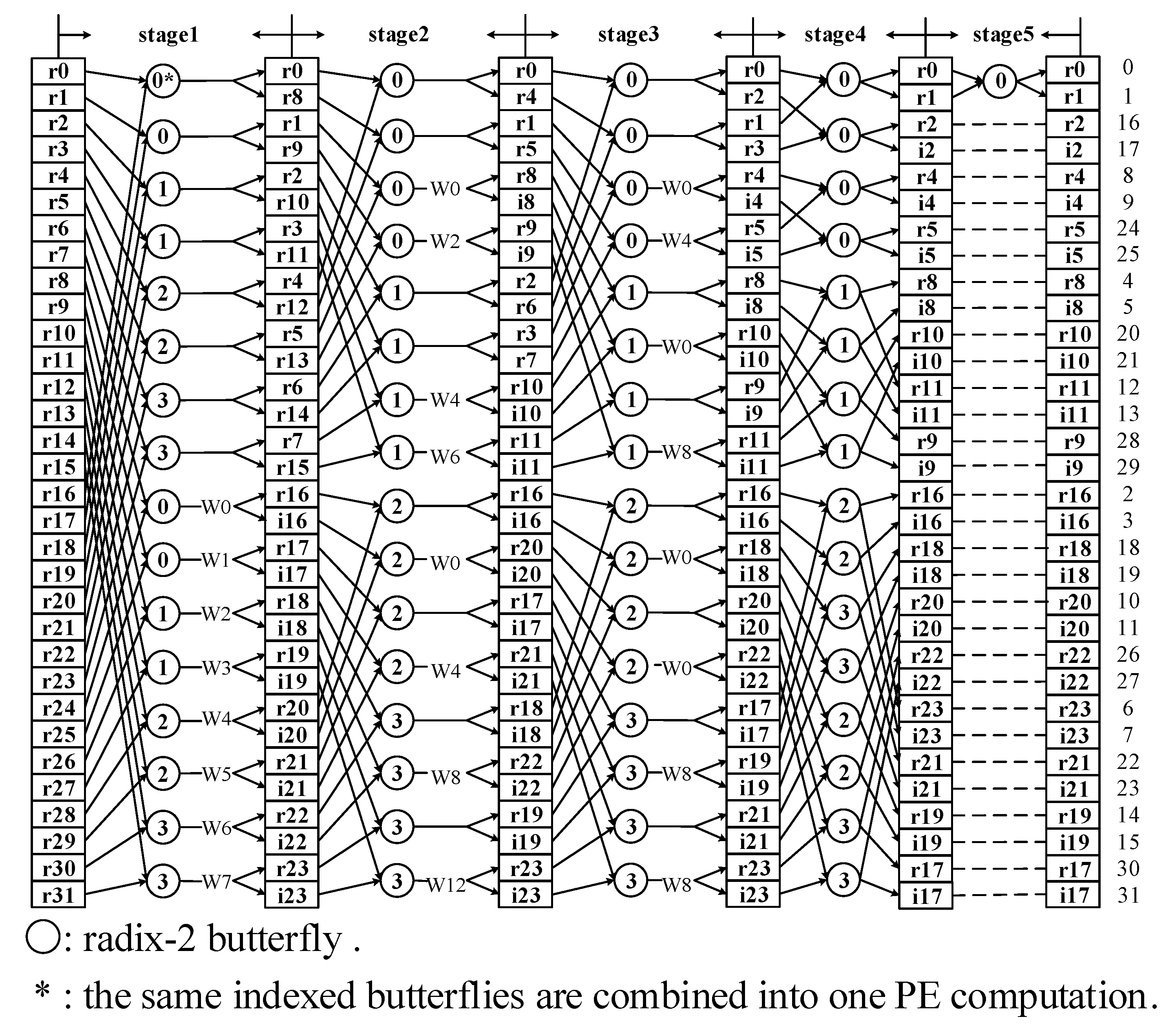
Figure 1, Ti(1) in stage 2 equals to 8. The strategy involves two steps. Step 1 is to float the real outputs in the upper half and to sink the complex outputs in the below half. Step 2 is to arrange the output with odd Ti to locate below those with even Ti. The load/store scheme is given as below:
L D ( i , k ) = { i 0 , i 1 , C n 4 . . . , C 1 , C 0 , i 2 } ,
S T ( i , k ) = { i 1 , C n 4 , . . . , C 1 , C 0 , i 2 , i 0 } .
To avoid bank conflict, the following conditions should be satisfied if i 1 i 2 , or k 1 k 2 :
m ( L D [ i 1 , k 1 ] ) m ( L D [ i 2 , k 2 ] ) ,
m ( S T [ i 1 , k 1 ] ) m ( S T [ i 2 , k 2 ] ) .
In Equation (5), the variation of i can be represented by L D 0 , L D n 2 and L D n 1 , where L D m is the mth bit of L D . Moreover, k can be represented by L D 1 , L D 2 , L D b 3 . According to Equation (4), L D 0 , L D 1 , L D 2 , L D b 3 , L D n 2 , and L D n 1 are mapped into the 0th to the ( n 1 ) th bit of m(LD) respectively. Therefore, the combinations of i and k are one-to-one mapped into m ( L D ) . Therefore, Equation (7) can be satisfied. Equation (8) can also be proved to be true. Thus, the conflict-free property of the bank address mapping scheme is proved in the first stage.
(2) The 2nd to the ( n 2 ) th stages: we use s to mark the stage index. In these stages, the load/store scheme can be summarized into two types: type I switches four complex data and type II switches four real data and two complex data. Type I will adopt strategy the same with stage 1. Type II only adopt its second step. Using the two strategies, we can derive that PE computations satisfying ( C < 2 n 1 & m o d ( C , 2 s 2 ) = = 0 ) are of type I and the rest are of type II. Moreover, the constant geometry in the [2, n− 2] stages can be maintained for any N. In all, for s = [ 2 , n 2 ] , the following loading/storing scheme is given in Algorithm 1. Similarly, the proposed load and store scheme can be proved to satisfy Equations (7) and (8), as all bits of i and k are mapped into divided bit-wise locations of the bank address.
Algorithm 1 Load and store scheme of the [ 2 , n 2 ] stages
if ( C < 2 n 1 & m o d ( C , 2 s 2 ) = = 0 ) then
   L D [ i , k ] = { C n 4 , i 1 , C n 5 , , C 0 , i 2 , i 0 } .
   S T [ i , k ] = { C , i 1 , i 2 , i 0 } .
else
   L D [ i , k ] = { C n 4 , i 0 , C n 5 , , C 0 , i 2 , i 1 } .
   S T [ i , k ] = { C , i 2 , i 1 , i 0 } .
end if
(3) The ( n 1 ) th stage: In this stage, symbols with the index L 1 = { a n 1 , a n 2 , , a w , 1 , a w 2 , , a 1 , a 0 } and L 2 = { a n 1 , a n 2 , , a w , 1 , a w 2 ˜ , , a 1 ˜ , a 0 } are managed in one computation and switched to obtain the frequency domain output in NAT order, where w = l o g 2 ( C ) and the tilde notation means negation operation. The load and store scheme is given in Algorithm 2. The variation of i and k can be represented by L D 0 , L D 1 , ..., L D b 2 , L D w + 2 , where w + 2 [ b 1 , n 2 ] . The above b-bits are one-to-one mapped into the b bits of m ( L D ) as shown in Equation (4). Similar analysis can be applied to the store scheme. Therefore, bank conflicts can be avoided in the ( n 1 ) th stage.
(4) The nth stage and the I/O mode: In the nth stage, only the first two data are involved and the store indices equal the load indices. In the I/O mode, the NAT and the REV representations are used in turn. If the input data is mapped in the NAT order, the bank mapping scheme at each stage is the same with Equation (4). When the input is in the REV order, the bank mapping scheme should be bit-reverse symmetric to Equation (4), which is given in Equation (9). Based on the symmetric property, the bank conflict in the I/O mode can be avoided.
m ( a ) = a 0 + ( i = b 1 n 1 a i ) 2 + i = 2 b 2 ( a n i a b i ) 2 i + ( i = 1 n b + 1 a i ) 2 b 1 .
Algorithm 2 Load and store scheme of the ( n 1 ) th stage
1:
w = l o g 2 ( C ) ;
2:
if w = = then
3:
L D ( i , k ) = i 2 ? { C , i 2 , i 0 , i 1 } : { C , i } ;
4:
S T ( i , k ) = { C , i } ;
5:
else
6:
k 1 = ( w p ) ? ( C 2 w ) : ( k 2 w ) ;
7:
L D ( i , k ) = 2 w + 3 + i 0 ˜ ( i 2 ( 2 w + 2 1 i 1 ˜ 2 k 1 ) + i 2 ˜ ( i 1 + 2 k 1 ) ) + i 0 ( i 2 ( 2 w + 3 1 i 1 ˜ 2 k 1 ) + i 2 ˜ ( 2 w + 2 + i 1 + 2 k 1 ) ) ;
8:
S T ( i , k ) = 2 w + 3 + i 1 ˜ ( i 2 ( 2 w + 2 1 i 0 ˜ 2 k 1 ) + i 2 ˜ ( i 0 + 2 k 1 ) ) + i 1 ( i 2 ˜ ( 2 w + 3 1 i 0 ˜ 2 k 1 ) + i 2 ( 2 w + 2 + i 0 + 2 k 1 ) ) ;
9:
end if

3.1.2. Periodicity of the Row Address Mapping Scheme

The address mapping scheme can be implemented by multiplying a with a non-singular linear transform matrix T s , f [9,10].
m r = T n × n a = U b × n V ( n b ) × n a .
m is the mapped bank address generated by U b × n and r is the row address generated by V ( n b ) × n . We use s and f to mark the stage index and the frame index, respectively. Specially, we consider s in the I/O mode to equal 0. Therefore, s [ 0 , n ] . U b × n is represented in Equations (4) and (9), corresponding to the NAT and REV forms, respectively. Then, the initial row address mapping scheme is given in Equation (3). Using the two initial conditions and the in-place property, all row address mapping schemes can be calculated in the following recursion manner.
We bring in two assist matrices Z 0 and Z 1 based on the locations of each bit of c in l d in stage 1 and stage 2 : n 2 , respectively. Based on Equation (5), Z 0 = I n ( b 2 : n 3 , : ) . Similarly, Z 1 ( = [ I n ( b 1 : n 3 , : ) ; I n ( n 1 , : ) ] by concatenating the ( b 1 ) th to the ( n 3 ) th rows and the ( n 1 ) th row of I n , where I n is an n × n identity matrix. As shown in Figure 1, three elementary permutation matrices Q 0 , Q 1 , and Q 2 can be used to describe the signal flow graph. We use Q 0 to define the bit-reverse permutation, Q 1 to define Equation (1), and Q 2 to define Equation (2).
Q 0 = [ I n ( : , 0 ) I n ( : , n 1 : 1 : 1 ) ] ; Q 1 = [ I n ( : , 1 : n 1 ) I n ( : , 0 ) ] ; Q 2 = [ I n ( : , 0 : 1 ) I n ( : , 3 : n 2 ) I n ( : , 2 ) I n ( : , n 1 ) ] ;
The three matrices summarize the bit permutations between the load and the store duration. If the bit permutation is an identity transformation, then the address mapping transformation in the previous stage can be reused in the next stage. As ( f = 1 4 ( Q 0 × ( t = 2 n 2 Q 2 ) × Q 1 ) = = I n , we obtain T s , f = = T s , f + 4 . Therefore, the row address appears as a periodic variation. The address mapping scheme is shown in Algorithm 3, where T 0 , 0 is defined using Equations (3) and (4). During implementation, the difference of the row address mapping scheme among stages and frames can be uniformed by an ( n b ) -bit cycle shift register. Using this method, the row address mapping implementation can be simplified.
Algorithm 3 Address mapping transform algorithm
1:
T 1 , f = T 0 , f T 0 , f ( 0 : b 1 , : ) Z 0 1 T 0 , f ( 0 : b 1 , : ) Z 0 Q 1 1 ;
2:
for s = 1 to n 3 do
3:
T s + 1 , f = T s , f T s , f ( 0 : b 1 , : ) Z 1 1 T s , f ( 0 : b 1 , : ) Z 1 Q 2 1 ;
4:
end for
5:
T n 1 , f = T n 2 , f ;
6:
T n , f = T n 1 , f ;
7:
T 0 , f + 1 = T n , f Q 0 ;
Table 1 is an instance of the address mapping scheme, in which one PE is used. Thus, the bank address is of 3-bit width and the row address is of ( n 3 ) -bit width. The address mapping scheme is periodic with the frame index and the period is 4. The bank address scheme only needs two formulae (the NAT and REV representations), which is very common in continuous-flow operations. The ( n 3 ) -bit row address mapping scheme can be realized with a ( n 3 ) -bit cycle shift register b and some fixed bits of a. Compared with prior address mapping schemes [4,5,7], the address mapping scheme is further controlled by a 2-bit frame index, which makes it a bit more complex. However, by considering the periodicity among the frames, the address mismatch between the input and output of the same frame is tolerated and the extra permutation is avoided.

3.2. Processing Element

The proposed PE comprises two sub-PEs in parallel. As no extra permutation circuit is needed in our design, each sub-PE uses a normal architecture the same as that used in [5], which is shown in Figure 4. The multiplexers in the proposed pe are controlled by S 1 to bypass the complex multiplication when the twiddle factor equal to 1. And the complex multiplication is trivial in the ( n 1 ) th to the nth stage.

4. Comparison

In this section, we compare the hardware complexity and computation cycles with prior memory-based architectures. The author of [4] presents a signal flow graph that only contains real-data path. Their PE handles four samples in parallel. Then [5] modifies the signal flow graph based on [4] and achieves time and resource efficiency. However, bank conflict occurs using their address scheme when considering concurrent I/O and normal-ordered I/O. Then [7] develops a continuous-flow memory-based RFFT architecture. However, their address mapping scheme still does not solve the bank conflicts. Instead, an extra permutation that needs a half stage computation time is brought in and extra RAMs and multiplexers are consumed.
Table 2 compares the proposed architecture with prior works. It can be concluded that the proposed architecture supports continuous-flow operation with the minimal computation cycles and the minimal memory resources when considering the same parallelism.
When compared to [4,5], we meet the constraint of the minimal computation cycle and the minimal multiplexer requirement. However, both [4,5] do not take continuous-flow and normal-order I/O into consideration. Their output order is scrambled, which is different from the normal order or the bit-reversal order, while each frame order in the our design is in normal-order. Using their method, if they consider normal-ordered I/O while still maintaining the in-place strategy, they need another N-word memories as the output buffer and an extra dedicated bit-reverse permutation circuit to reorder their frame output according to [3]. Therefore, 3 N single-port memories are needed in their design when considering the same constraint, while 2 N single-port memories are needed in our design.
When compared with [7], N / 2 B computation cycles are saved. The time-reduced factor is calculated as 1 / ( 2 l o g 2 N 1 + 16 / N ) . The factor is 6.64 % , 4.76 % , and 4.35 % when N is 256, 2048, and 4096, respectively, which will be useful in time-critical applications [2]. We consider that a B-port multiplexer can be realized with ( B 1 ) 2-port multiplexers. When considering the hardware complexity, the ( 10 × 2 b 2 ) -word memories and ( 6 × 2 b 1 ) 2-port multiplexers are saved when compared with [7].
Table 3 compares the synthesis results, which are obtained using ISE14.5 tool on a Xilinx Virtex-7 field-programmable gate array, i.e., XC7VX485T. As 8 datasets are handled in parallel, the 16 RAMs are used and each has a depth of N / 8 . The adders, subtracter, and multipliers are designed to use the same computation latency between our design and [7]. The synthesis results show our design outperforms the design in [7]. Although our address module is a bit more complex than [7], the saving of the extra permutation circuit gains resource and frequency efficiency.
Besides, as our PE can be designed to consume 0 cycle latency while at least 1 cycle latency is needed in [7], single-port memory is used in our design while [7] uses dual-port memory. According to [11], the area of single-port memory is about 56 % less than the dual one. Therefore, our memory requirement is less than [7].

5. Conclusions

This article presents a memory-based RFFT architecture based on constant geometry. The proposed addressing mapping scheme meets the constraint of concurrent I/O, normal-ordered I/O, in-place operation and parallel processing. When considering the continuous-flow operation, the minimal computation cycle and the minimal memory requirements are achieved.

Author Contributions

Conceptualization, M.Y., Z.M., F.Y., and Q.X.; methodology, M.Y., Z.M., F.Y., and Q.X.; investigation, M.Y., Z.M., F.Y., and Q.X.; validation, M.Y., Z.M., F.Y., and Q.X.

Funding

This research received no external funding.

Conflicts of Interest

The authors declare no conflict of interest.

References

  1. Cheng, M.H.; Chen, L.C.; Hung, Y.C.; Yang, C.M. A real-time maximum-likelihood heart-rate estimator for wearable textile sensors. In Proceedings of the 2008 30th Annual International Conference of the IEEE Engineering in Medicine and Biology Society, Vancouver, BC, Canada, 20–25 August 2008; pp. 254–257. [Google Scholar]
  2. Islam, M.; Biswas, T.; Saad, A.M.; Haque, C.A.; Yusuf, M.S.U. A Non-invasive Heart Rate Esitimation Approach from Photoplethysmography. In Proceedings of the International Joint Conference on Computational Intelligence, IJCCI 2018, Dhaka, Bangladesh, 14–15 December 2018; pp. 383–394. [Google Scholar]
  3. Jo, B.G.; Sunwoo, M.H. New continuous-flow mixed-radix (CFMR) FFT Processor using novel in-place strategy. IEEE Trans. Circuits Syst. I Regul. Pap. 2005, 52, 911–919. [Google Scholar] [CrossRef]
  4. Ayinala, M.; Lao, Y.; Parhi, K.K. An In-Place FFT Architecture for Real-Valued Signals. IEEE Trans. Circuits Syst. II Express Briefs 2013, 60, 652–656. [Google Scholar] [CrossRef]
  5. Ma, Z.G.; Yin, X.B.; Yu, F. A Novel Memory-Based FFT Architecture for Real-Valued Signals Based on a Radix-2 Decimation-In-Frequency Algorithm. IEEE Trans. Circuits Syst. II Express Briefs 2015, 62, 876–880. [Google Scholar] [CrossRef]
  6. Garrido, M.; Parhi, K.K.; Grajal, J. A Pipelined FFT Architecture for Real-Valued Signals. IEEE Trans. Circuits Syst. I Regul. Pap. 2009, 56, 2634–2643. [Google Scholar] [CrossRef] [Green Version]
  7. Mao, X.B.; Ma, Z.G.; Yu, F.; Xing, Q.J. A Continuous-Flow Memory-Based Architecture for Real-Valued FFT. IEEE Trans. Circuits Syst. II Express Briefs 2017, 64, 1352–1356. [Google Scholar] [CrossRef]
  8. Xing, Q.J.; Ma, Z.G.; Xu, Y.K. A Novel Conflict-Free Parallel Memory Access Scheme for FFT Processors. IEEE Trans. Circuits Syst. II Express Briefs 2017, 64, 1347–1351. [Google Scholar] [CrossRef]
  9. Harper, D.T. Block, multistride vector, and FFT accesses in parallel memory systems. IEEE Trans. Parallel Distrib. Syst. 1991, 2, 43–51. [Google Scholar] [CrossRef]
  10. Sorokin, H.; Takala, J. Conflict-free parallel access scheme for mixed-radix FFT supporting I/O permutations. In Proceedings of the 2011 IEEE International Conference on Acoustics, Speech and Signal Processing (ICASSP), Prague, Czech Republic, 22–27 May 2011; pp. 1709–1712. [Google Scholar]
  11. Ayinala, M.; Brown, M.; Parhi, K.K. Pipelined Parallel FFT Architectures via Folding Transformation. IEEE Trans. Very Large Scale Integr. VLSI Syst. 2012, 20, 1068–1081. [Google Scholar] [CrossRef]
Figure 1. Proposed signal flow graph of a 32-point real-valued FFT (RFFT).
Electronics 08 01042 g001
Figure 2. Proposed reverse representation.
Electronics 08 01042 g002
Figure 3. Proposed high-level RFFT architecture using P processing elements (PEs).
Electronics 08 01042 g003
Figure 4. Architecture of the kth sub-PE.
Electronics 08 01042 g004
Table 1. Address mapping scheme with 8 parallelism.
FrameBankRow Address
IndexAddressStage 0Other Stages
0{ i = 2 n 1 a i , i = 1 n 2 a i , a 0 } { a n 1 , b [ n 4 : 1 : 1 ] } { d , a 1 , b [ n 5 : 1 : 1 ] }
2 { a 1 , d , b [ n 5 : 1 : 1 ] } { b n 4 , a n 1 , b [ n 5 : 1 : 1 ] }
1{ i = 1 n 2 a i , i = 2 n 1 a i , a 0 } { d , a n 1 , b [ 0 : 1 : n 6 ] } { a n 1 , d , b [ 0 : 1 : n 6 ] }
3 { b n 4 , a 1 , b [ 0 : 1 : n 6 ] } { a 1 , b n 4 , b [ 0 : 1 : n 6 ] }
b = r o r ( a [ n 2 : 2 ] , s ) . r o r means cycle right shifting a [ n 2 : 2 ] by s bits and s = m i n ( s , n 2 ) . d = a 1 a n 1 b n 4 .
Table 2. Comparison of the RFFT processors.
Proposed[7][4][5]
Parallelism B ( = 2 b ) Support b 3 b 2 b 2 b 2
PE 2 b 1 complex adders and 2 b 2 complex multipliers
2 Port Multiplexers 2 2 b + 1 + 3 × 2 b 1 2 2 b + 1 + 9 × 2 b 1 2 2 b + 1 + 5 × 2 b 1 2 2 b + 1 + 3 × 2 b 1
Memory 2 N × W ( 2 N + 10 × 2 b 2 ) × W 2 N × W 2 N × W
Computation Cycles N ( l o g 2 N 1 ) / B + 1 N ( l o g 2 N 0.5 ) / B + 1 N ( l o g 2 N ) / B + 1 N ( l o g 2 N 1 ) / B + 1
Continuous FlowYesYesNoNo
Normal-ordered I/OYesYesNoNo
Table 3. Comparison of the experimental results.
NOccupied SlicesRAMFreq (MHz)
PEAddr 1 Total
[7]256623152130116490
20483151411431
40963501446(dual)415
Ours25645028799516493
20483311274483
40963761334(single)483
1 The address control module.

