A Compact 5 GHz Power Amplifier Using a Spiral Transformer for Enhanced Power Supply Rejection in 180-nm CMOS Technology


Division of Electronics and Electrical Engineering, Dongguk University, Seoul 04620, Korea
*
Author to whom correspondence should be addressed.
Electronics 2019, 8(9), 1043; https://doi.org/10.3390/electronics8091043
Submission received: 15 August 2019
/
Revised: 9 September 2019
/
Accepted: 16 September 2019
/
Published: 17 September 2019
(This article belongs to the Special Issue Microwave Integrated Circuits Design and Application)
Abstract
:We present a compact 5 GHz, class A power amplifier (PA) applicable for a wireless combo-chip that supports multiple radio systems in 180 nm CMOS technology. The proposed two-stage linear PA consists of a cascode input stage with a transformer-based balun, combined with a balancing capacitor as the load, where the single-ended signal is converted into the balanced output and a second-stage, class A push–pull amplifier with another transformer-based balun, which efficiently combines the output power differentially to drive a single-ended 50 Ω load. The proposed single-ended PA with an internal balanced configuration can achieve a power supply rejection ratio of 9.5 to 65.9 dB at 0.1 to 3.5 GHz, which is around a 12 to 37 dB improvement compared to a conventional single-ended PA with the same power gain. The results show that the proposed PA has a gain of 15.5 dB, an output-referred 1 dB gain compression point of 13 dBm, an output intercept point of 22 dBm with a 5 MHz frequency offset, an output saturated power of 15.4 dBm, and a peak power-added efficiency of 15%. The implemented PA consumes a DC current of 72 mA under 1.8 V supply. The core chip size is 0.65 mm2 without pads.
1. Introduction
In wireless communication for mobile applications, a power amplifier (PA) is an essential block in the radio frequency (RF) front-end. The PA must not only deliver the necessary power efficiently, but also should be robust towards the common mode interferences from other blocks around it. Notably, a robust design to cope with interference should be accomplished in multiple radio applications, since various wireless systems are combined in a single chip. A PA requires various design trade-offs between the supply voltage, output power, power efficiency, and linearity, in order to meet the desired specifications. Many researchers have put enormous effort and showed significant interest in improving the linearity and the efficiency of Pas, while lowering power consumption with low cost [1,2]. Although a switch-mode PA theoretically has 100% of the drain efficiency, it cannot be directly applicable to the modulation scheme, which utilizes the amplitude of the transmitting signal. To overcome this issue, a polar power amplifier has been introduced using a mixed-signal technique [3]. However, the size of the mixed-signal, 2.4 GHz PA is bulky (3.06 mm2), due to the extra RF digital-to-analog converter for the polar operation. Moreover, the switch-mode PA may generate a large amount of interference from the digitally-oriented blocks, which can seriously contaminate sensitive analog/RF blocks that are integrated into the same chipset.
The linearity of the PA directly affects the whole performance of a modern wireless system. In IEEE 802.11a wireless LAN applications, orthogonal frequency-division multiplexing (OFDM) is typically used to provide fast data rates at 5 GHz; this requires a high linear power amplifier, since the linearity of the power amplifier determines the data rates of the communication [4]. Contrary to the switch-mode PA, the linear PA can support any modulation scheme without limitations. Among them, the class A PA has the highest linearity and lowest distortion, both of which are essential characteristics for wireless communication [1,2]. With a differential configuration, the class A PA can also achieve an excellent common-mode rejection, with relatively good power-added efficiency (PAE) with an inductive load. Therefore, class A PAs have been widely used in practice, specifically in WLAN transceivers [5]. Unfortunately, a typical single-ended PA has a poor common-mode rejection, which is not directly applicable to a combo-chip with multiple wireless transceivers integrated into a single chipset.
In this paper, we present a compact class A PA for operation at 5 GHz. Since the power supply noise can combine with the RF signal and reduce the performance of the power amplifier [6], the proposed PA utilizes an on-chip transformer balun to achieve improved power supply rejection ratio, as well as a compact design. At the output of the first stage, the balun with a balancing shunt capacitor converts the single-ended signal to a differential one, which also works as the inter-stage matching network, while the second balun combines the output power and converts the output port from the differential to the single-ended configuration. With this architecture, the proposed PA can achieve substantially improved RF power supply rejection under multiple radio-system scenarios while delivering consistent performance, with a saturated power output of 15.4 dBm and a peak PAE of 15%. The implemented PA consumes only 0.65 mm2 without pads, owing to the transformer-based compact baluns.
2. Circuit Design
The schematic diagram of the proposed PA is illustrated in Figure 1. Input matching is performed with C1, L1, and source degeneration inductor LS. C1 and L1 are also used together as a biasing circuit. The input stage of the PA is a cascode structure, to improve the voltage gain of the driving amplifier. A compact on-chip balun is realized by modifying a symmetric inductor whose half of a winding coil is magnetically coupled to the other half, in order to convert a single-ended signal to a balanced output by connecting the center tap to the power supply node. The converted differential output from the balun of the first stage is amplified by the second-stage, differential, common-source amplifier, having the primary coil of the second transformer as the load. Then the differential output is converted to the single-ended output, using the transformer-based balun. Therefore, when we assume a reasonable input and output matching condition, the magnitude of the transducer power gain (GT) in differential mode at the center frequency (fo = ωo/2π) can be approximated as
where Ro is the source and load impedance; Qi = 1/ωCgs1Ro, QT1 is the quality factor (Q-factor) of the first transformer (TF1); ηM, and ηT are the power efficiency of the input (L-matching) and output (TF2) matching networks, respectively [7]; the resistance transformation ratio r = Ro/Re{Zin} = 1; k is the magnetic coupling coefficient; and QT2P and QT2S are the Q-factors of the primary and secondary coil of the TF2, respectively.
The symmetric spiral inductor is used as a balun to provide a differential signal to the second stage. In addition, it suppresses the RF interferences from the supply node [8]. For the designed balun, LT1P and LT1S are both 1.425 nH, and their resistances are 4.372 Ω (quality factor (Q) = 10.2) and 4.744 Ω (Q = 9.4), respectively; the difference in Q of the symmetric inductor is because LT1S includes two bridges with a thin metal layer (M5), as presented in Figure 1. The thickness of M5 is 0.525 μm, while that of layer M6 is 2.1 μm, which means that LT1S is more resistive than LT1P. Note that symmetric inductors are widely used instead of two spiral inductors, because this saves on the circuit area and results in a higher Q [9].
A tunable balancing capacitor of 410 fF is employed at one of the TF1 output ports to emulate parasitic capacitance from the drain node of the cascode structure, so that the power supply rejection ratio (PSRR) and the drain efficiency can be significantly improved. The power supply rejection ratio (PSRR) is given by
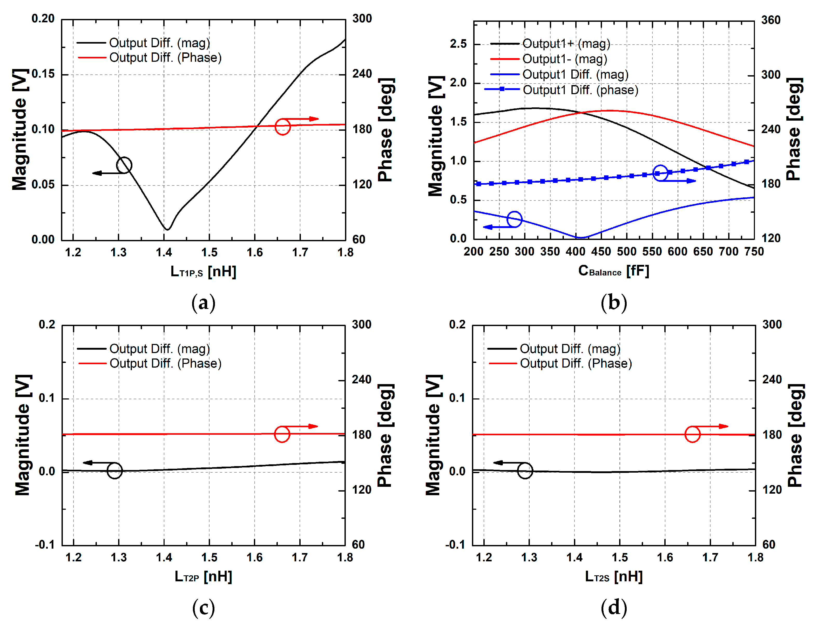
The value of CBalance is chosen to balance out the voltage at each differential node, which improves the achieved balance of the output. Figure 2 shows the parametric sweep of the symmetric inductor (LT1P,S), the balancing capacitance (Cbalance), and the inductance of the output transformer (LT2P,S), which shows that other circuit parameters, except Cbalance, are not critical to the interference suppression from the supply. By sweeping CBalance from 200 fF to 750 fF, it indicates that 410 fF of CBalance optimally balances the output voltage at the differential node, while providing approximately 180° of phase difference.
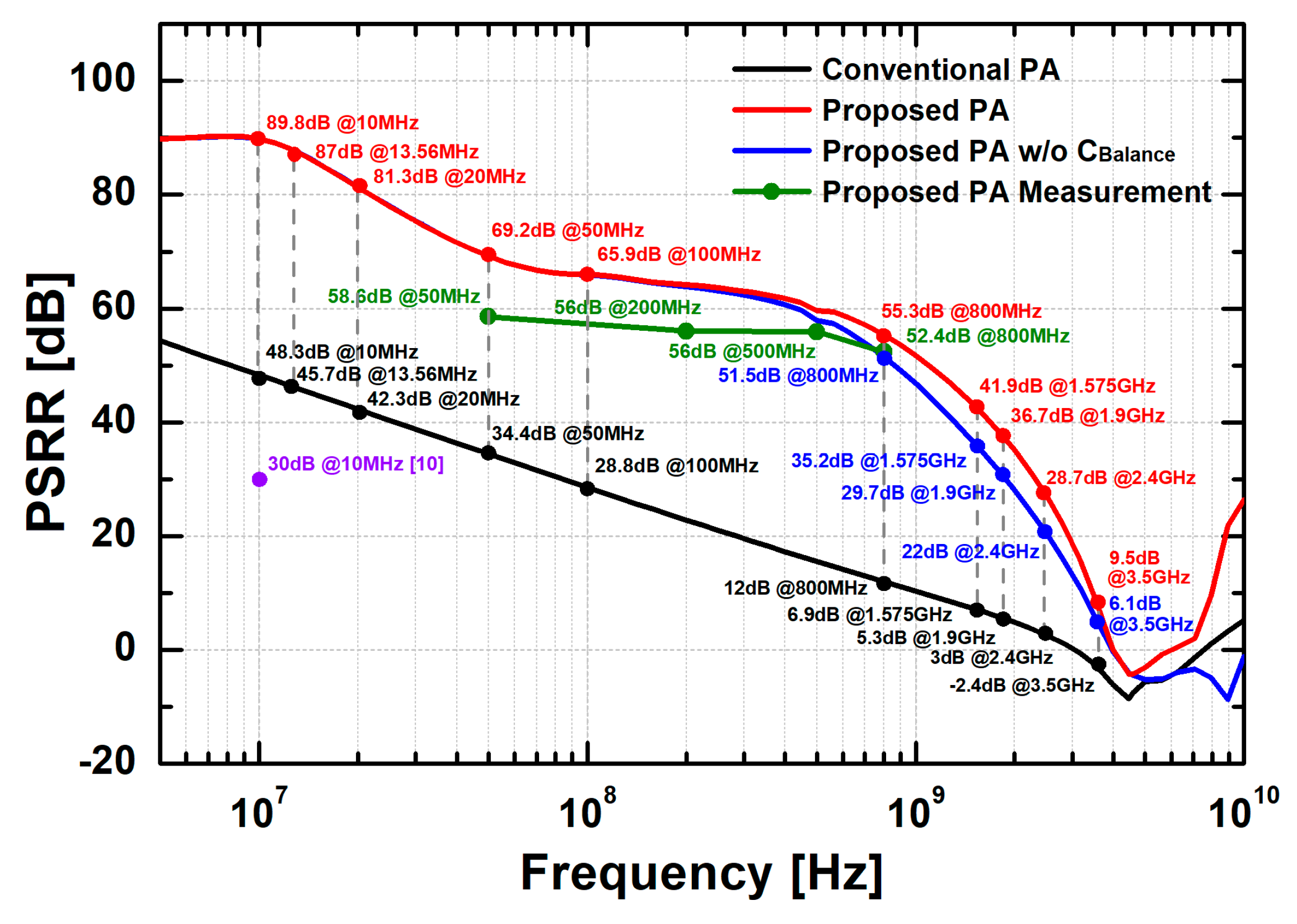
Figure 3 shows the simulated PSRR comparison between a conventional PA, the proposed PA, and the proposed PA without CBalance. At the operating frequencies of the various wireless communication systems that can be integrated into a single chip, the designed single-to-differential conversion network with a balancing capacitor, as well as the symmetric inductor having a center-tap to VDD, achieves relatively reasonable PSRR in the inter-stage. This is important because blocks like power amplifiers are fragile to external interference [10]. Moreover, it is difficult to improve the PSRR for an RF regime with low dropout regulators (LDO).
The output stage is configured as a differential, common-source amplifier to enhance the power gain; it can achieve better common-mode rejection from the supply, which is represented by the PSRR. The differential stage suffers from common-mode interference if its differential pair becomes asymmetric, and has a finite tail current source impedance [9]. A 1:1 transformer is used to achieve output impedance matching in the second stage. The transformer operating as a balun converts the differential signal to a single-ended one at the output. The parallel capacitors CT1 and CT2 are optimized to minimize the loss between the primary and secondary inductors. The values of LT2P, LT2S, CT1, and CT2 in Figure 1 are 1.01 nH, 1.16 nH, 810 fF, and 300 fF, respectively. The resistance of LT2P is 3.9 Ω (QT2P = 7.5), and that of LT2S is 4.25 Ω (QT2S = 7.9). When designing the output 1:1 transformer-based balun, power contours and mismatch circles are used with the load-pull method in Cadence SpectreRF to achieve optimal power matching at the output. The output transformer is implemented based on the extracted output impedance for optimal power matching [11,12].
3. Measurement Results
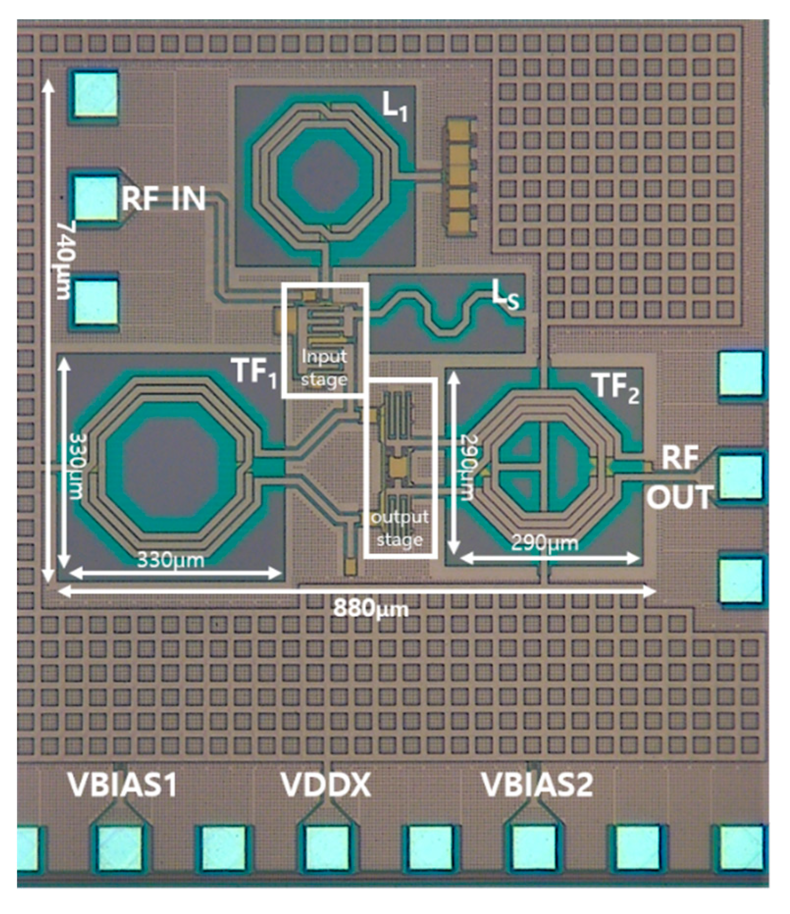
Figure 4 shows a photograph of the implemented power amplifier with a chip size of 0.65 mm2 and without pads, while Figure 5 shows the measurement and probing setup of the proposed PA. The S-parameter measurements were performed with Keysight N5224A PNA. VBIAS11 and VBIAS2 were set to 0.95 V. The total DC current consumption was 72 mA under a 1.8 V voltage supply, which made the total DC power consumption 130 mW. Both the measured and simulated S-parameters are shown in Figure 6. There was a frequency shift of 0.2 GHz, which equates to roughly 4.5% error in the center frequency. The maximum value of S21 was 15.5 dB at 4.6 GHz. The 3 dB bandwidth of the implemented PA was 1 GHz (from 4.1 GHz to 5.1 GHz).
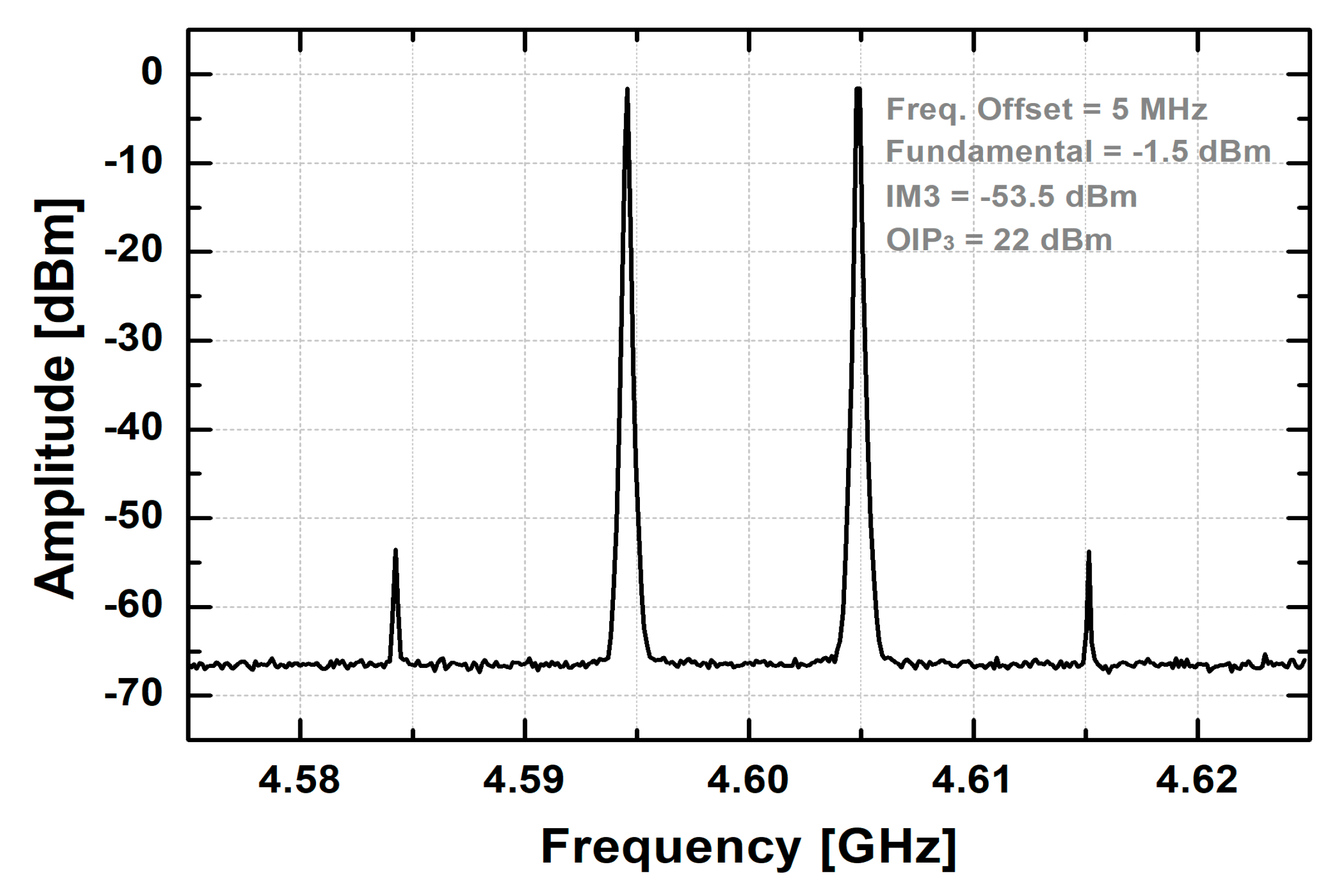
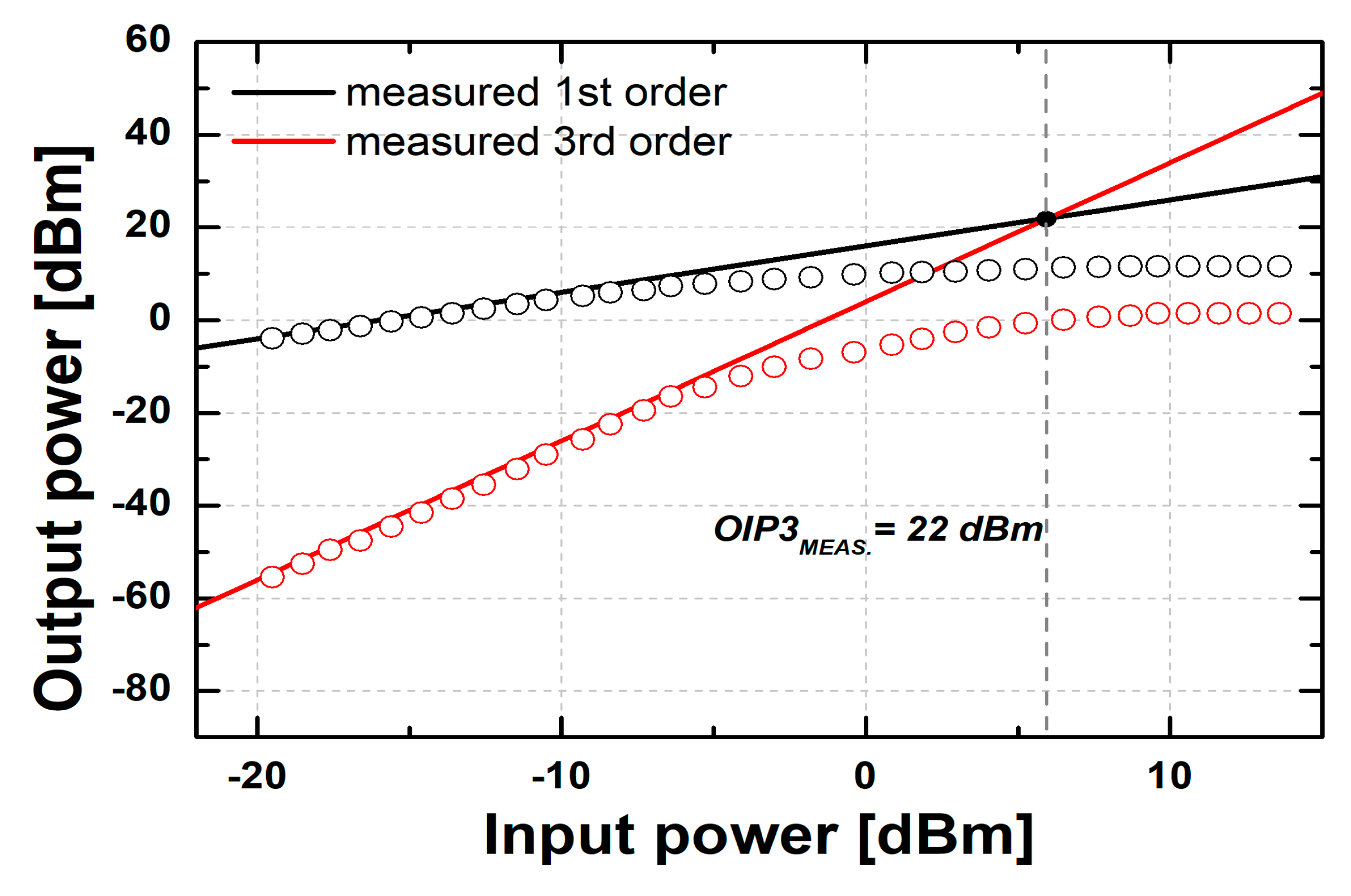
The output-referred 1 dB compression point (OP1dB) and the PAE were measured with an Agilent E4405B spectrum analyzer and an Agilent 83623B signal generator. The results show that the OP1dB was 13 dBm, PSAT was 15.4 dBm, and the peak PAE was 15% when the input power was −1.5 dBm, as depicted in Figure 7. Figure 8 presents the measured output signal of the proposed PA when intermodulation was performed with a 5 MHz frequency offset, while Figure 9 shows the measured third-order intercept point (IP3) of the implemented PA (the simulated input-referred IP3 (IIP3) was 8 dBm); the measured output-referred IP3 (OIP3) was 24.5 dBm, while the measured IIP3 was 6.5 dBm and the measured OIP3 was 22 dBm.
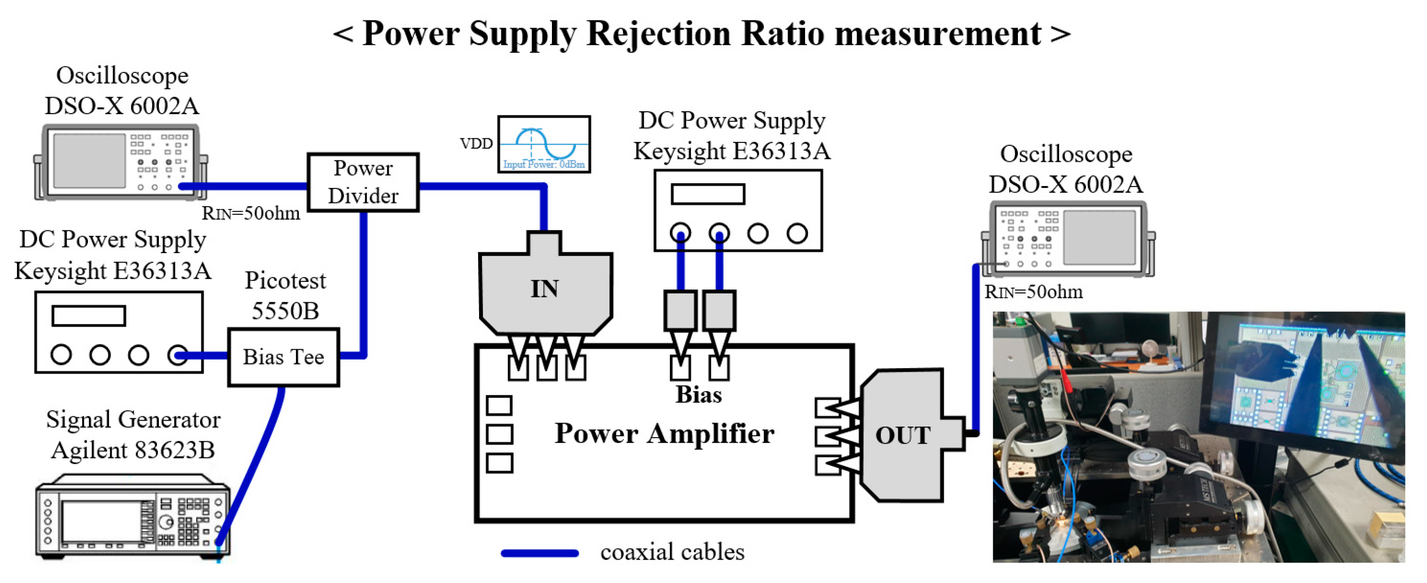
Figure 10 illustrates the measurement setup for the PSRR presented in Figure 3 [13]. A reference AC signal and 1.8 V supply voltage are simultaneously applied to the VDD pad through the bias tee (Picosecond 5550B) and ground-signal-ground (GSG) probe tip. The measured PSRR of the proposed PA at 50 MHz~800 MHz is around 58.6~52.4 dB, which demonstrates the substantial improvement in the PSRR of the proposed PA for the RF regime.
Table 1 summarizes the comparison of our work with previously published PAs; the figure of merit (FoM) is given by
where f is the center frequency, PRfout is the output power and Area is the chip occupation size. The FoM of the proposed design is 45 (dBm∙GHz2)/mm2, which demonstrates a comparable PA performance while providing a substantially improved PSRR at the frequencies used for various wireless communications.
4. Conclusions
A compact, 5 GHz power amplifier (PA) was implemented with a transformer-based balun in an 180 nm CMOS process. With the proposed single-ended PA having an internally operating, in-balanced configuration, we could achieve a compact PA with a dramatically improved PSRR in the RF regime, for a combo-chip integrated with multiple wireless transceivers. The implemented PA achieved a PAE of 15% and a PSAT of 15.4 dBm. The proposed PA could be applicable to combo-chips, when considering the dramatically reduced common-mode interference with a comparable RF performance, as well as its compact size. The chip consumes 130 mW under a supply voltage of 1.8 V, with a chip occupancy of 0.65 mm2.
Author Contributions
Data curation, Y.-J.C.; supervision, J.-D.P.; validation, H.N.; writing—original draft, Y.-J.C.; writing—review and editing, J.-D.P.
Funding
This research was funded by the Dongguk University Research Fund of 2019 (S-2019-G0001-00059); the Korea Institute of Energy Technology Evaluation and Planning (KETEP) and the Ministry of Trade, Industry & Energy (MOTIE) of the Republic of Korea (No. 20194030202320).
Acknowledgments
This work was supported by the Dongguk University Research Fund of 2019 (S-2019-G0001-00059); the Korea Institute of Energy Technology Evaluation and Planning (KETEP) and the Ministry of Trade, Industry & Energy (MOTIE) of the Republic of Korea (No. 20194030202320).
Conflicts of Interest
The authors declare no conflict of interest. The funders had no role in the design of the study; in the collection, analyses, or interpretation of data; in the writing of the manuscript, or in the decision to publish the results.
References
- Reynaert, P.; François, B.; Kaymaksüt, E. CMOS RF PA Design: Using Complexity to Solve the Linearity and Efficiency Trade-off. In Proceedings of the 2009 IEEE International Symposium on Radio-Frequency Integration Technology (RFIT 2009), Singapore, 9–11 December 2009; pp. 207–212. [Google Scholar]
- Srirattana, N.; Raghavan, A.; Heo, D.; Allen, P.E.; Laskar, J. Analysis and Design of a High-efficiency Multistage Doherty Power Amplifier for Wireless Communications. IEEE Trans. Microw. Theory Tech. 2005, 53, 852–860. [Google Scholar] [CrossRef]
- Winoto, R.; He, M.; Lu, Y.; Signoff, D.; Chan, E.; Lin, C.-H.; Loeb, W.; Park, J.; Lin, L. A WLAN and Bluetooth Combo Transceiver with Integrated WLAN Power Amplifier, Transmit-receive Switch and WLAN/Bluetooth Shared Low Noise Amplifier. In Proceedings of the 2012 IEEE Radio Frequency Integrated Circuits Symposium, Montreal, QC, Canada, 17–19 June 2012; pp. 395–398. [Google Scholar]
- Singh, A.; Kaur, H. Non Linearity Analysis of High Power Amplifier in OFDM System. Int. J. Comput. Appl. 2012, 37, 37–41. [Google Scholar] [CrossRef]
- Su, D.; Zagari, M.; Yue, P.; Rabii, S.; Weber, D.; Kaczynski, B.; Mehta, B.; Singh, K.; Mendis, S.; Wooley, B. A 5 GHz CMOS Transceiver for IEEE 802.11a Wireless LAN. In Proceedings of the 2002 IEEE International Solid-State Circuits Conference. Digest of Technical Papers, San Francisco, CA, USA, 7 February 2002; pp. 92–449. [Google Scholar]
- Stauth, J.T.; Sanders, S.R. Power Supply Rejection for RF Amplifiers: Theory and Measurements. IEEE Trans. Microw. Theory Tech. 2007, 55, 2043–2052. [Google Scholar] [CrossRef] [Green Version]
- Aoki, I.; Kee, S.D.; Rutledge, D.B.; Hajimiri, A. Distributed active transformer-a new power-combining and impedance-transformation technique. IEEE Trans. Microw. Theory Tech. 2002, 50, 316–331. [Google Scholar] [CrossRef] [Green Version]
- Wei, P.; Tsai, M.; Hsu, S.; Shen, C.; Wu, T. An Electromagnetic Bandgap Structure Integrated With RF LNA Using Integrated Fan-Out Wafer-Level Package for Gigahertz Noise Suppression. IEEE Trans. Microw. Theory Tech. 2018, 66, 5482–5490. [Google Scholar] [CrossRef]
- Razavi, B. RF Microelectronics, 2nd ed.; Prentice-Hall: Upper Saddle River, NJ, USA, 2012. [Google Scholar]
- Loikkanen, M.; Kostamovaara, J. High PSRR Class AB Power Amplifier. In Proceedings of the 2006 NORCHIP, Linkoping, Sweden, 20–21 November 2006; pp. 71–74. [Google Scholar]
- Pedro, J.C.; Nunes, L.C.; Cabral, P.M. A Simple Method to Estimate the Output Power and Efficiency Load-Pull Contours of Class-B Power Amplifiers. IEEE Trans. Microw. Theory Tech. 2015, 63, 1239–1249. [Google Scholar] [CrossRef]
- Pengelly, R.; Saffian, M. Load Pull Simulation Speeds Design of Wideband High-Efficiency PAs [Application Notes]. IEEE Microw. Mag. 2016, 17, 42–53. [Google Scholar] [CrossRef]
- El-Nozahi, M.; Amer, A.; Torres, J.; Entesari, K.; Sanchez-Sinencio, E. High PSR Low Drop-Out Regulator With Feed-Forward Ripple Cancellation Technique. IEEE J. Solid-State Circuits 2010, 45, 565–577. [Google Scholar] [CrossRef]
- Le, V.-H.; Han, S.-K.; Lee, S.-G. A Low Power Driver Amplifier for Unlicensed 2.4 GHz Band. IEICE Trans. Electron. 2011, 94, 120–123. [Google Scholar] [CrossRef]
- Lin, K.-C.; Chiou, H.-K.; Wu, P.-C.; Ko, C.-L.; Tsai, H.-H.; Juang, Z.-L. A 28-dBm Pout 5-GHz CMOS Power Amplifier using Integrated Passive Device Power Combining Transformer. In Proceedings of the Asia-Pacific Microwave Conference Proceedings (APMC), Seoul, Korea, 5–8 November 2013; pp. 766–768. [Google Scholar]
- Zhang, W.; Khoo, E.-Z.; Tear, T. A Low Voltage Fully-integrated 0.18 um CMOS Power Amplifier for 5 GHz WLAN. In Proceedings of the 28th European Solid-State Circuits Conference, Florence, Italy, 22–26 September 2002; pp. 215–218. [Google Scholar]
- Eo, Y.-S.; Lee, K.D. A Fully Integrated 24-dBm CMOS Power Amplifier for 802.11a WLAN Applications. IEEE Microw. Wirel. Compon. Lett. 2004, 14, 504–506. [Google Scholar] [CrossRef]
- Kurniawan, T.A.; Yoshimasu, T. A 2.5-GHz 1-V High Efficiency CMOS Power Amplifier IC with a Dual-Switching Transistor and Third Harmonic Tuning Technique. Electronics 2019, 8, 69. [Google Scholar] [CrossRef]
Figure 1.
A schematic diagram of the proposed power amplifier (PA).

Figure 2.
The magnitude and phase of the symmetric inductor as a function of the optimization of (a) LT1P,S, (b) CBalance, (c) LT2P, and (d) LT2S.
Figure 2.
The magnitude and phase of the symmetric inductor as a function of the optimization of (a) LT1P,S, (b) CBalance, (c) LT2P, and (d) LT2S.

Figure 3.
The simulated power supply rejection ratio (PSRR) of a conventional PA, the proposed PA (excluding CBalance), and the simulated and measured PSRR of the proposed PA as a function of frequency, with the reported PSRR of the radio frequency (RF) of the PA in [10].
Figure 3.
The simulated power supply rejection ratio (PSRR) of a conventional PA, the proposed PA (excluding CBalance), and the simulated and measured PSRR of the proposed PA as a function of frequency, with the reported PSRR of the radio frequency (RF) of the PA in [10].

Figure 4.
A microphotograph of the proposed PA.

Figure 5.
(a) Measurement and (b) probing setup of the proposed PA.
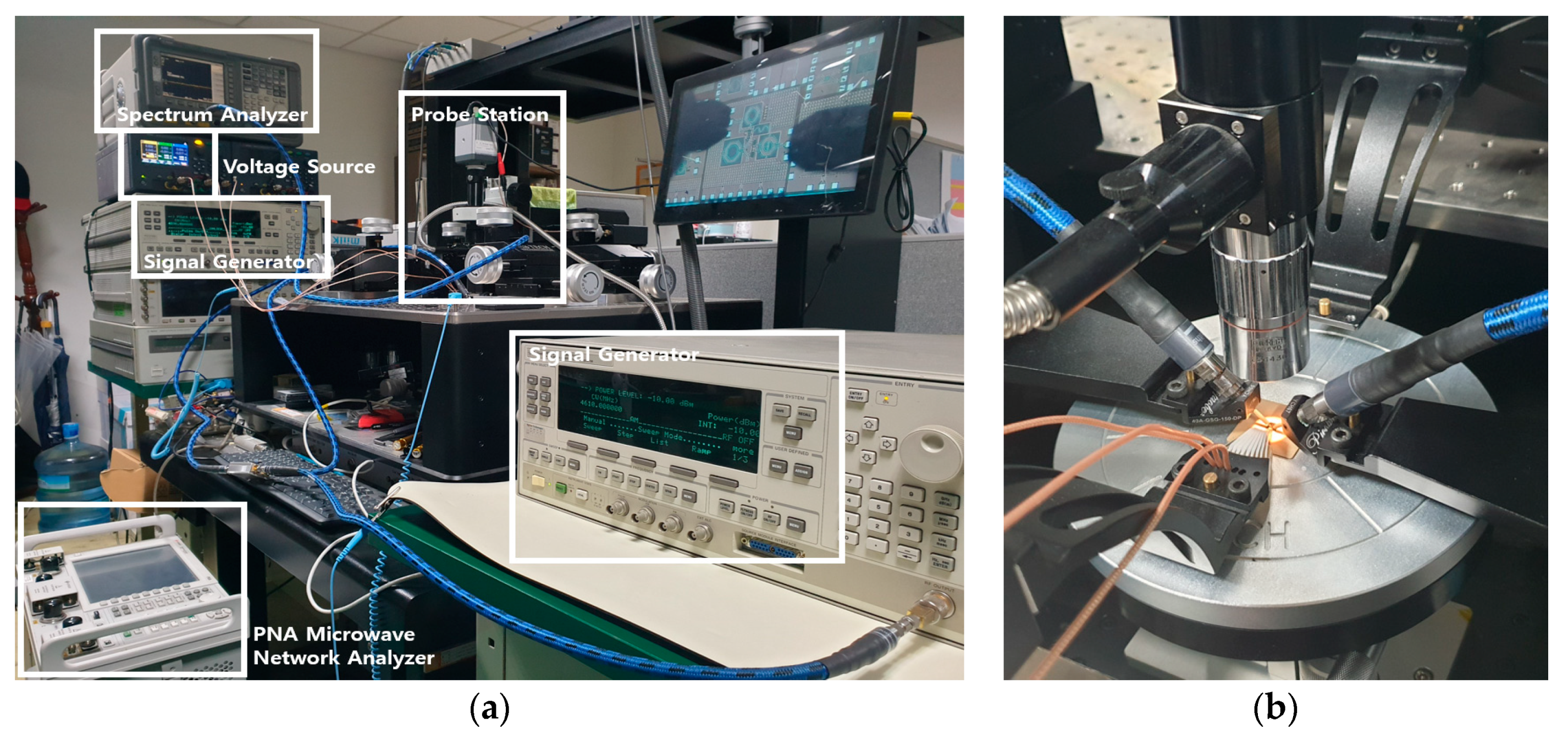
Figure 6.
The simulated and measured S-parameters of the proposed PA.
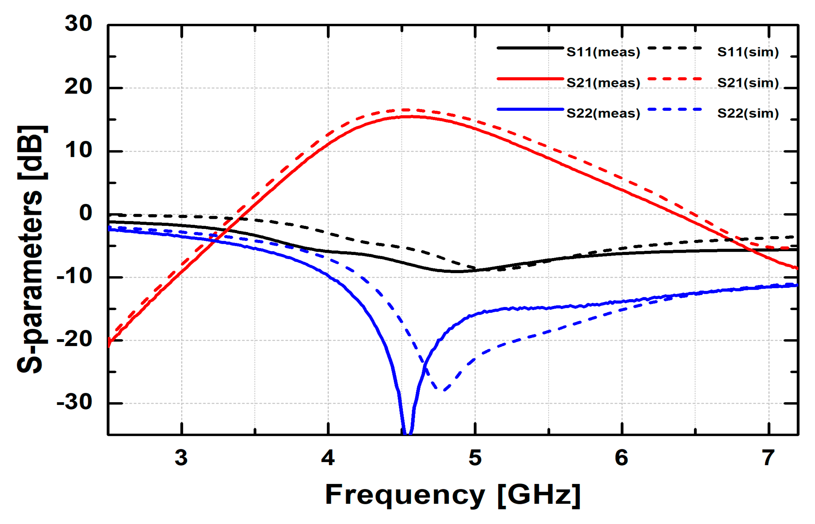
Figure 7.
The simulated and measured gain, output power (POUT), and power-added efficiency (PAE) of the implemented PA.
Figure 7.
The simulated and measured gain, output power (POUT), and power-added efficiency (PAE) of the implemented PA.
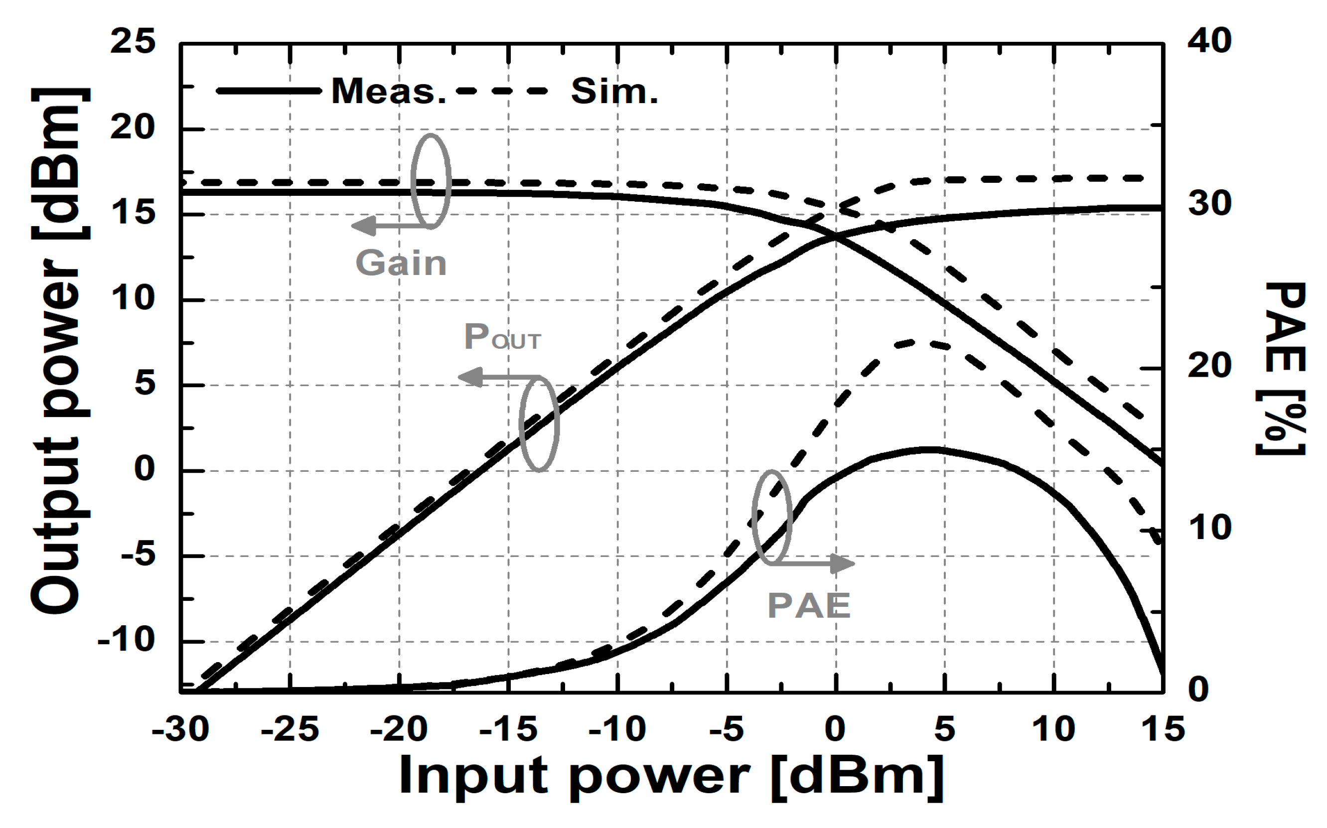
Figure 8.
The output signal of the proposed PA, measured with the E4405B spectrum analyzer.

Figure 9.
The measured output-referred third-order intercept point (OIP3) of the proposed two-stage PA.
Figure 9.
The measured output-referred third-order intercept point (OIP3) of the proposed two-stage PA.

Figure 10.
The PSRR measurement setup.


Table 1.
Comparison of the power amplifiers.
| PA | This Work | [3] | [6] | [10] | [14] | [15] | [16] | [17] | [18] |
|---|---|---|---|---|---|---|---|---|---|
| Technology [nm] | 180 | 55 | 180 | 350 | 180 | 180 | 180 | 180 | 180 |
| Frequency [GHz] | 4.1–5.1 | 2.4 | 2.4 | 10.6 MHz | 2.4 | 5.8 | 5 | 5 | 2.5 |
| Supply Voltage [V] | 1.8 | 3.3 | 1.8 | 3 | 1.8 | 1.8 | 1.8 | 1.8 | 1 |
| PSAT [dBm] | 15.4 | 29 | 15 | - | 5 | 26.7 | 17.4 | 24.1 | 10.1 |
| PAE(1) [%] | 15 | - | - | - | 20 | 19 | 27.1 | 13 | 34.5 |
| OP1dB [dBm] | 13 | 27.5 | - | - | 4 | 24.2 | 15.4 | 21.8 | 8 |
| OIP3(2) [dBm] | 22 | -15 | - | - | 15 | - | 25 | - | - |
| PSRR [dB at 10 MHz] | 82.5 | - | 25 | 30 | - | - | - | - | - |
| Area [mm2] | 0.65 | 6.6 | 1.96 | - | 0.8 | 1.92 | .84 | 1.8 | - |
| FoM* [(dBm∙GHz2)/mm2] | 45 | - | - | - | 21.6 | - | 51.5 | - | - |
(1) , (2) , (3)
© 2019 by the authors. Licensee MDPI, Basel, Switzerland. This article is an open access article distributed under the terms and conditions of the Creative Commons Attribution (CC BY) license (http://creativecommons.org/licenses/by/4.0/).
Share and Cite
MDPI and ACS Style
Choe, Y.-J.; Nam, H.; Park, J.-D. A Compact 5 GHz Power Amplifier Using a Spiral Transformer for Enhanced Power Supply Rejection in 180-nm CMOS Technology. Electronics 2019, 8, 1043. https://doi.org/10.3390/electronics8091043
AMA Style
Choe Y-J, Nam H, Park J-D. A Compact 5 GHz Power Amplifier Using a Spiral Transformer for Enhanced Power Supply Rejection in 180-nm CMOS Technology. Electronics. 2019; 8(9):1043. https://doi.org/10.3390/electronics8091043
Chicago/Turabian StyleChoe, Young-Joe, Hyohyun Nam, and Jung-Dong Park. 2019. "A Compact 5 GHz Power Amplifier Using a Spiral Transformer for Enhanced Power Supply Rejection in 180-nm CMOS Technology" Electronics 8, no. 9: 1043. https://doi.org/10.3390/electronics8091043
Note that from the first issue of 2016, this journal uses article numbers instead of page numbers. See further details here.