1. Introduction
The inexorable reduction of fossil fuels and non-renewable energy sources feeds the wind of change that leads to substantial use of renewable energy to such a point that many countries have now defined a roadmap for replacing polluting traditional energy sources with clean and renewable plants [
1]. Among renewable sources, photovoltaic energy is a primary choice because of the energy density that affects every part of the Earth, the maturity of conversion technologies, and the low cost/watt.
Despite its advantages, photovoltaics suffers from the discontinuity of the resource and the inability of large accumulations, if not at very high costs. Furthermore, existing solar technologies have very low returns compared to other production facilities. Therefore, the need to maximize the yield of individual generators is of primary importance, regardless of the grid connection, in order to reduce the need to use large and extensive surfaces of ground or roofing, as in the case of solar systems, or expensive and, in general, over-dimensioned plants.
With this in mind, smart converter devices provide a suitable response to the need to maximize the produced energy. They work increasing the instantaneous production also responding to variations in weather and working operating conditions [
2]. There are many open points still to be solved or improved to ensure an optimal system response, even in variable conditions such as partial shading, non-uniformity of PV panel temperatures, dust effects for solar panels [
3], and the discontinuity of the wind [
4].
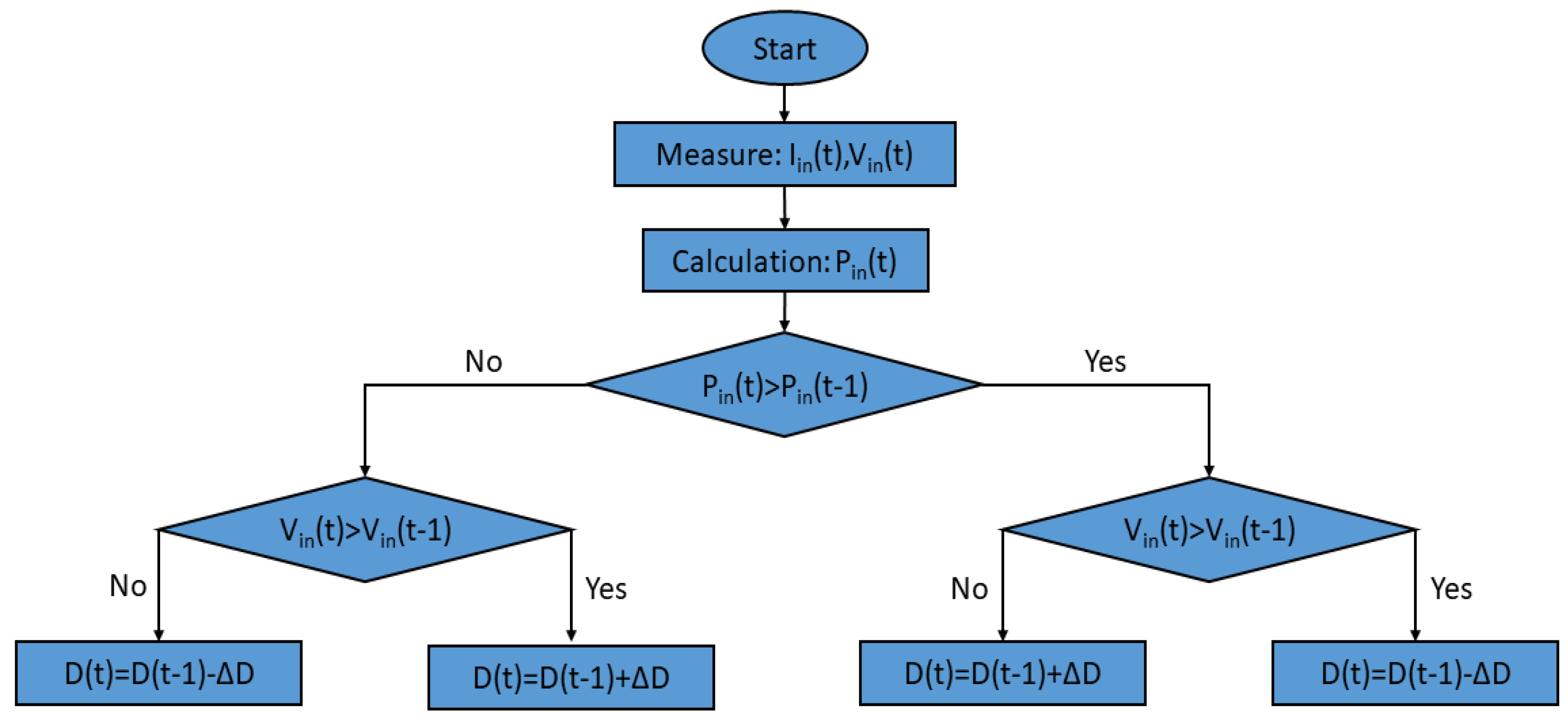
The efficiency of various MPPT algorithms has been compared in several papers [
5], showing that perturbation and observation (P&O) and incremental conductance (IC) methods are simple and often applied, despite their slow tracking and low utilization efficiency. Minor modifications of the P&O and IC have been proposed by several authors [
6] to reduce the known drawbacks of the aforementioned algorithms. Fuzzy and neural network techniques are used nowadays and show an increased efficiency [
7].
In this scenario, algorithms are mainly computer-simulated, e.g., using specific engineering software tools (Matlab [
8], Spice [
9]) and environments that provide easily deployable algorithms; discussions on efficiency and results comparison are always pursued on different hardware platforms, leading to barely comparable conclusions and results due to the heterogeneity of the hardware used and the analysis conditions.
A possible solution to overcome these problems consists in the development of a flexible platform exploitable for the implementation, debugging, and the testing of smart converters algorithms. This topic has acquired prominence since these conversion systems are widely applied in current energetic contexts. In the literature, different papers propose open-access platforms. Currently, none of them have been dedicated to smart DC/DC converters.
In [
10], a control platform for soft-switching multi-level inverters is proposed. The paper presents an FPGA-based prototyping tool for modular DC/AC converters. A verification of concept case is reported; the implemented hardware is not open or accessible.
In this work, we propose a novel open-source electronics platform for research, industrial, and educational purposes. The platform has been conceived and released as an open hardware and software instrument for the academic and industrial communities. It can be used by students for a deep comprehension of DC/DC converters operating and control modes. Researchers can take advantage of the proposed architecture for modulation and control strategies validation. It can be also used by designers for a rapid project check. The platform itself is proposed as a benchmark in the development and testing of different smart converters algorithms.
This hardware configuration and embedded software functions are freely available to benefit from users’ community improvements.
The novelty of this approach also consists in the cloud connectivity feature. In fact, the platform is equipped with a Wi-Fi communication module to enable data gathering and dispatching. Users can access a suitable application programming interface to validate algorithms online and control techniques changing the smart converter functional parameters (duty cycle, switching frequency, dead time, algorithms, etc). In addition, the Wi-Fi communication module permits one to implement diagnostic functions to verify smart converters behavior during the design process, but also to monitor and acquire operating data in functioning mode. This feature is crucial, especially when the system is being tested in the field.
So, the proposed platform represents an innovative hardware and a valid pre-prototyping tool for DC/DC converters.
The board is populated with a 5000 LookUp Table (LUT) Complementary Metal-Oxide Semiconductor (CMOS) FPGA integrated circuit (iCE40UP5K UltraPlus
TM, Lattice Semiconductor, [
11]), an embedded DSPic (dsPIC33EPXXGS50X, Microchip Technology INC., [
12]), and a Silicon Labs (WGM110 [
13]) Wi-Fi module.
The VHDL (Very High Speed Integrated Circuits Hardware Description), the C-code for the DSPic, and the Wi-Fi module are provided under the terms and conditions of the MIT License [
14].
The schematic, layout, and bill of materials are also provided on the same public repository on the popular platform Github [
15], at the web address [
16], released under Creative Commons Share-alike 4.0 International License [
17].
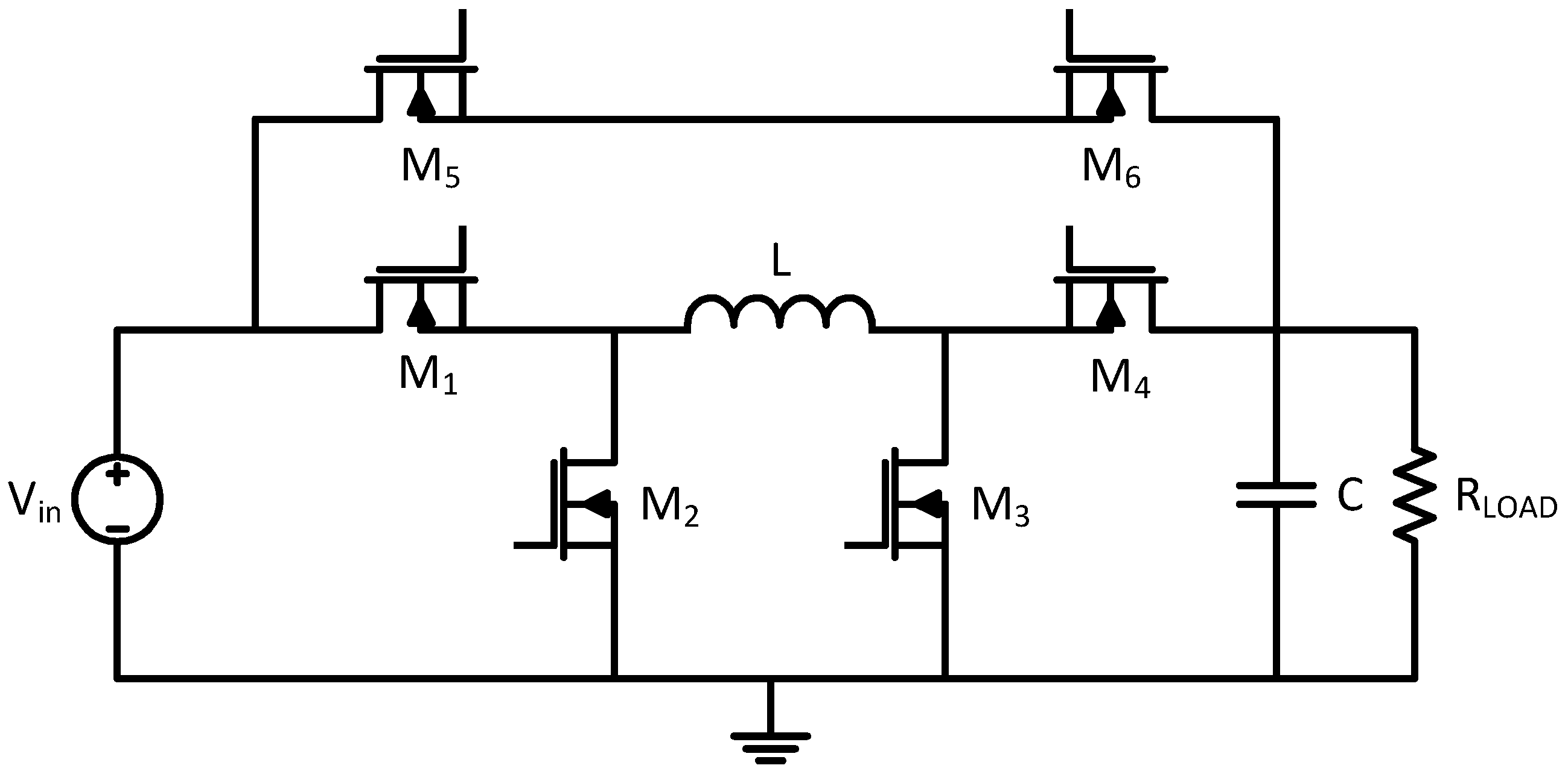
The FPGA generates high-frequency PWM signals for controlling Metal-Oxide-Semiconductor Field-Effect Transistors (MOSFETs) with appropriate frequency, dead-time, and duty cycle, and implements bootstrap and interleaved control logic.
The microcontroller acquires currents and voltages from the power circuit and has a bidirectional communication with FPGA and Wi-Fi module.
Both the two logical blocks could implement power conversion algorithms: the FPGA by using high-speed circuits that implement logic at a hardware level and the microcontroller by executing a firmware code within its own CPU. This novel architecture allows the flexibility of algorithm implementation, deployable in hardware, software, or in combined mode.
The separation between the power board and the logic board allows the comparison of different architectures, different device technologies, and the usage of interleaving options.
The sum of the already developed software parts constitute a new software framework, based on FPGA, uC, and Wi-Fi module source codes and their interoperability.
The basic motivation behind the conception and release as an open hardware and software instrument for the academic and industrial communities is to benefit from the researchers’ community improvements. An open platform, according to the opinion of the authors, would allow more developers to design smart converters and MPPTs, focusing on algorithms instead of electronics.
The authors focused, as a proof of concept, on the deployment of a solution tailored for photovoltaic applications up to 450W. The designed system is capable of implementing MPPs accurately, allowing for the testing of different current and voltage-controlled MPPT algorithms.
The versatility of the solution, despite this implementation, does not limit the possibility to be adapted to several renewable energies, with the only limits being the maximum power of 450 W and wide voltage input and output ranges of 15–70 V.
The maximum pulse width modulation (PWM) frequency used for feeding the gates of the H-Bridge topology is 250 kHz, and the minimum dead time is 83 ns. These values are limited by MOSFETs used in the power circuit (IPB038N12N3G by Infineon [
18,
19]). However, the platform can work up to a maximum frequency of about 500 kHz with a minimum dead time of 21 ns.
The paper is organized as follows:
Section 2 describes the architecture of the provided open hardware platform, the circuital blocks, and the most important electronic components used.
Section 3 and 4 discuss the design phase and the layout outcome of the main logic board and the power shield board, respectively. In
Section 5, experimental results are shown for the P&O algorithm.
Section 6 provides a better interpretation and guideline of the platform use, while conclusions are drawn in
Section 7.
3. Main Logic Board Design and Layout
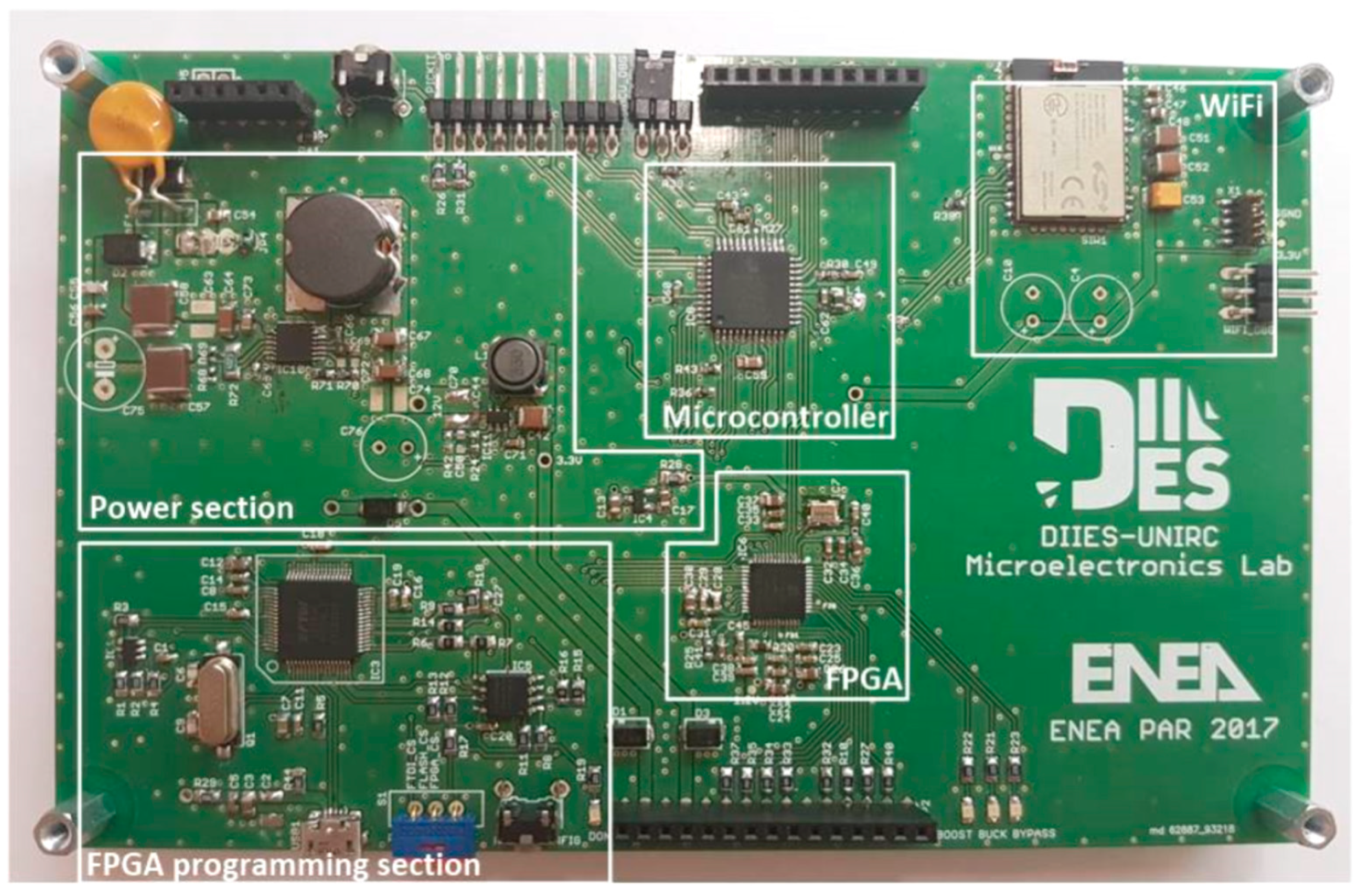
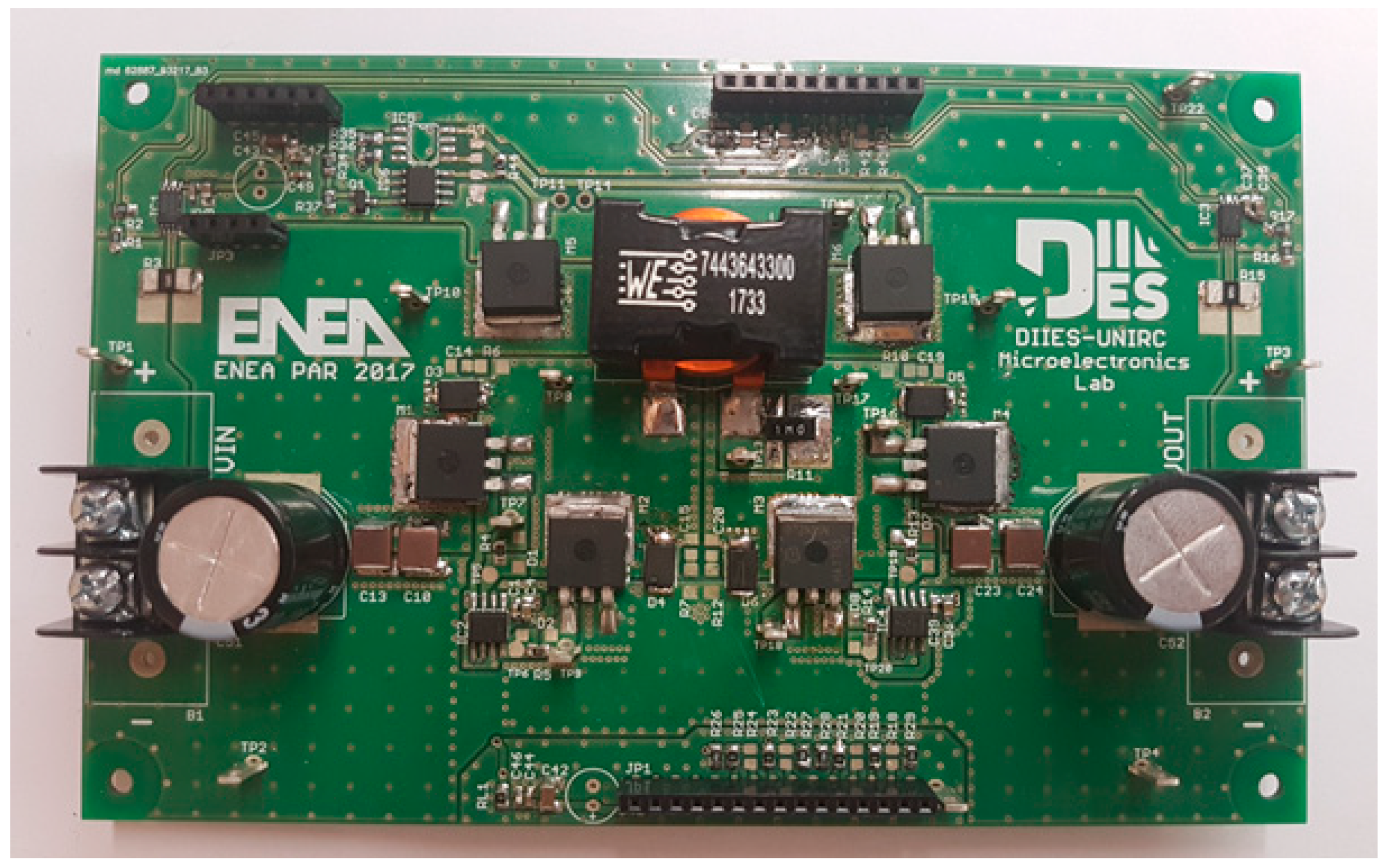
In this section, design and realization of the main logic board (MLB) are described. The board, shown in
Figure 4, is used to control the power shield (PS) and the Wi-Fi communication. It consists of a power section where there are
A step-down converter (LM5161 [
23]) that allows to generate 12 V from the input voltage (output voltage of the photovoltaic source);
A step-down converter (TPS561208 [
24]) that converts the 12 V into 3.3 V;
A CMOS low dropout (LDO) voltage regulator (MCP1700-1202 [
25]) that generates 1.2V from 3.3V for the FPGA core.
Another section consists of the components for the programming of the FPGA. It is realized with an USB connector and an FTDI chip (FT2232 [
26]) that allows one to program an external FLASH memory (SST25VF080B [
27]), used for storing the bitmap file of the FPGA, while, as previously mentioned, the main components of this board are a Lattice Semiconductor FPGA (iCE40UP5K [
11]), a Microchip Technology INC. dsPIC (dsPIC33EP64GS504 [
12]), and a Silicon Labs (WGM110 [
13]) Wi-Fi module.
In the following, these three main components and their firmware are described more in detail.
3.1. FPGA
iCE40UP5K is an ultra-low power FPGA with a sleep current of about 35 μA and 1–10 mA active current. The characteristics of the device are reported in [
11]. In the FPGA, commonly used to make high-frequency circuits, it is possible to instantiate a control unit that works as a coprocessor of the microcontroller. Its use allows one to obtain a high data processing speed and the addition of logical blocks without hardware changes. The FPGA firmware starts with the acquisition of the digital values of input and output current and voltage of the MPPT, received from the microcontroller through a serial communication. Direction and number of connections are detailed in
Table 1. Moreover, it acquires some PWM parameters, i.e., frequency, duty cycle, and deadtime. Subsequently, it calculates the MOSFETs duty cycles through the implementation of the MPPT’s algorithm and it generates the PWM signals of (M
1, M
2, M
3, and M
4). In the meanwhile, proper values of frequency, duty cycle, and dead time, and some debug data, are sent to the microcontroller.
The minimum resolution of the signals generated by the FPGA is 21 ns, related to the maximum frequency of the used hardware (50 MHz). Using a 7-bit, mod-100 counter, the generation of PWM could lead to a 500 kHz signal for feeding the MOSFET’s gate. In practice, using a Si power board, the maximum PWM frequency has been limited to 250kHz, using an 8-bit, mod-200 counter. The switching frequency can be calculated as .
At the same time, the FPGA controls the two MOSFET M5 and M6 used to bypass the DC/DC converter. In particular, the two MOSFETs are on for 1 min when the voltage output of the converter remains almost equal to the voltage input (0.95 Vin < Vout < 1.05 Vin) for almost 15 s. Moreover, the microcontroller can force the bypass mode when the circuit has a malfunction. Finally, the FPGA allows the control of one or more power shield (interleaved condition) in order to improve the performance of the circuit, e.g., reducing the voltage output ripple and improving the circuit reliability.
3.2. Microcontroller
The microcontroller is the control center of the logic board and interfaces with the FPGA chip, which generates the fast control signals of the MOSFETs, and with the Wi-Fi module for communicating parameters and measurements to other devices.
The microcontroller acquires the analog signals from the sensors and sends them, through a custom communication protocol, to the FPGA, managing moreover its reset and enable signals.
The microcontroller chosen for the realization is the dsPIC33EP64GS504 [
12]. It is a 16-bit microcontroller from Microchip and is part of the digital signal processing family, and it has some specific functions for the control and management of switching circuits and power conversion, including high speed 12-bit Analog to Digital Converter (ADC) with 5 ADC SAR cores, flexible and independent ADC trigger sources, and comparators with dedicated 12-bit digital-to-analogue converter (DAC). The microcontroller is set to use its internal RC oscillator and PLL to achieve a working frequency of 42.38 MHz.
In the microcontroller choice, particular importance has been given to the speed and accuracy characteristics of the analog to digital controller module. In fact, the specific application requires the simultaneous operation of several ADC modules, to measure accordingly the current and voltage and then calculate the relative power.
The microcontroller has four independent modules plus a shared one; the dedicated modules can sample the signal at the same time, using a common trigger signal to trigger them simultaneously; this allows us to perform a synchronous and instantaneous sampling of the various power card measurements. The readings of the ADC modules are appropriately averaged with a high number of samples to reduce the measurement noise. The dedicated cores of the ADC have been used for the most important signals for the operation of the MPPT, and in particular currents and input voltage. The analog inputs were set as follows:
AN0: VOUT (core 0)
AN1: VIN (core 1)
AN2: I_IN_1 (core 2)
AN3: I_IN_2 (core 3)
AN4: TEMP_1 (shared core)
AN5: TEMP_2 (shared core)
AN12: I_OUT_1 (shared core)
AN14: I_OUT_2 (shared core)
The analog comparator is used to detect when input and/or output voltages and/or currents exceed the design limits. When the limits are exceeded, an interrupt is generated that allows one to intervene in the duty cycle of the converter, limiting current/voltage and bringing the system back to the expected operating range. Each comparator is internally connected to the same inputs as the ADC converter, and is always active, even during normal operation of the ADC module.
To transfer to the FPGA the information obtained from the ADC, a communication protocol is implemented that transfers five words (VIN, VOUT, I_IN, IOUT_1, and IOUT_2) of 16 bits each on five separate pins, and two control signals (START and CLOCK). Transmission of the operating parameters is made serially with a 32-bit word that contains duty cycle MOSFET M1, duty cycle MOSFET M2, 4-bit dead time selection, three frequency selection bits, and one bit for forcing the duty from the outside.
The microcontroller receives the operating status of the FPGA via the SPI protocol. Three 16-bits words are transferred, the first four bits of which indicate the type of data sent, while the remaining 12 bits contains the actual data (MOSFETs duty cycle, dead time, frequency, and operating mode).
The microcontroller also sends three additional control signals to the FPGA to (1) reset the FPGA chip, (2) enable the FPGA, and (3) force the bypass condition.
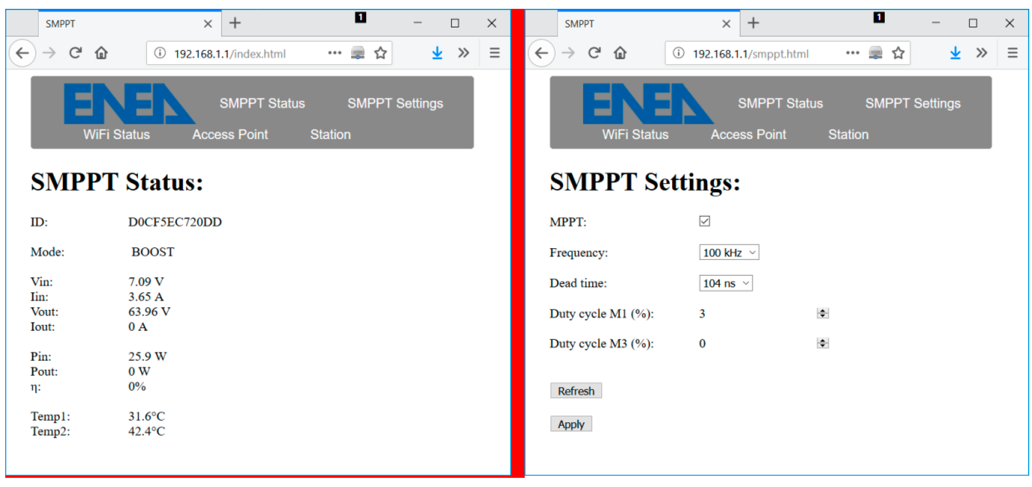
The microcontroller and the Wi-Fi module communicate via the UART serial interface. Periodically, the microcontroller sends to the Wi-Fi module all the current, voltage, temperature, operating mode, and system parameters measurements, which are stored in the Wi-Fi module and displayed in its internal web server interface, or communicated via appropriate APIs to other devices.
In addition, the Wi-Fi module can send, through the same interface, operating parameters to the microcontroller (duty cycle, frequency, dead time, and duty cycle) to customize the operation of the device remotely.
To debug the system, a UART transmission and reception protocol has been implemented, through which, with a connection to the PC, it is possible to set the operating parameters of the card (duty cycle, frequency, dead time, duty cycle, and bootstrap) and observe the trend of the current, voltage, power, and temperature measurements of the power cards.
For programming the microcontroller, the MPLAB X software, an integrated development environment from Microchip, was used. The source code was written in C and compiled using the XC16 compiler.
3.3. API Wi-Fi
A web server was implemented, to enable querying of the Wi-Fi module for data gathering and dispatching coming from/to another device on the same network. Thanks to custom developed application programming interface (API), using GET/POST command over hypertext transfer protocol (HTTP), whose result is a JSON object, it is possible to establish different policy and strategies of data collection, supervision, and network optimization in a smart and effectively way. The APIs implementation and explanation are provided on the public repository [
16].
The read status API has been implemented to retrieve the status of the system, thus responding with eight different parameters and measurements.
For the sake of completeness, we provide the following detailed CURL description:
The query response, provided in JSON format, is the following:
{
“mac”: “xxxxxxxxxxxx”,
“mode”: [int, bit0=BOOST, bit1=BUCK, bit2=BYPASS],
“temp1”: [signed int, °C x 100],
“temp2”: [signed int, °C x 100],
“meas”: {
“Vin”: [int, Volt x 100],
“Vout”: [int, Volt x 100],
“Iin”: [int, Ampere x 1000],
“Iout”: [int, Ampere x 1000]
}
}
The read settings API has been implemented as a GET request too, providing information about the actual PWM frequency, dead time, and duty cycles.
The write setting API allows the users to modify the settings in use and it is recalled using the following:
with the value to write that should be put in the body of the request.
“item” can be:
mppt MPPT ON/OFF [0–1] -> 0 = dc/dc, 1 = mppt
freq switching frequency [0–7] -> {100,80,120,150,175,200,225,250} kHz
dt dead time [0–15] -> {104,21,41,62,83,104,125,145,166,187,208,229,250,271,291,312} ns
m1 duty cycle MOSFET M1 [0–4095]
m3 duty cycle MOSFET M3 [0–4095]
In the
Figure 5, a possible graphical representation of the information obtained from the
read status and
read setting APIs is provided.
5. Experimental Results
Experimental results are shown for P&O and IC algorithms and compared to state-of-the-art outcomes from similar platforms.
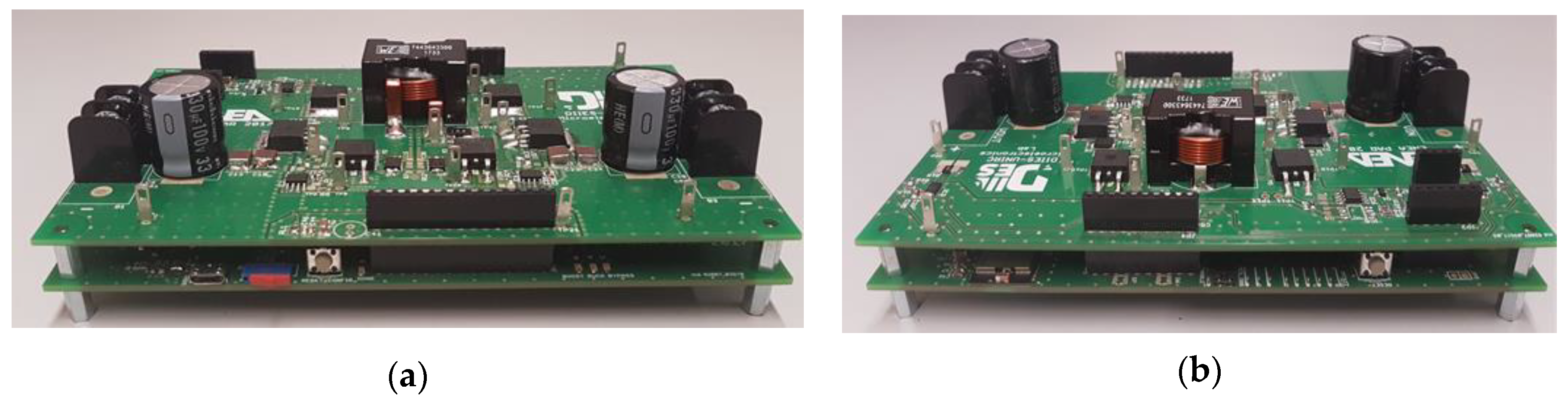
In
Figure 7 two images of the realized MPPT are shown. The bottom board is the main logic board, on which the power board is fitted by strip line connectors.
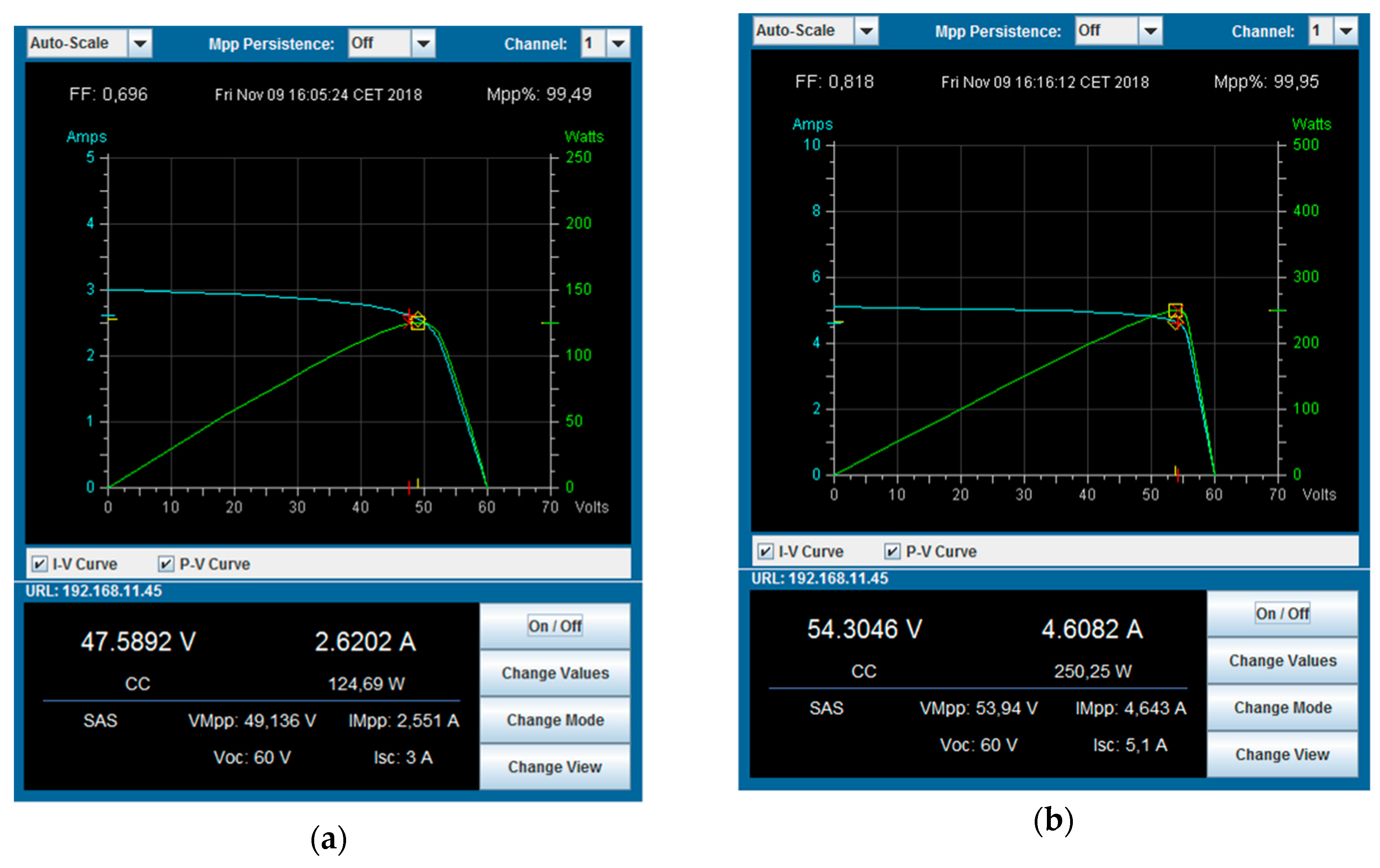
A series of tests were performed using the modular solar array simulator from Agilent Technologies in order to characterize the goodness of the MPP tracking, the speed of convergence, and stability over time.
The results were obtained with various MPP from 50 W to 450 W, with different combinations of V
OC and I
SC. In
Figure 8, the tracking measurements at 125 and 250 W are shown. The MPP is achieved with good accuracy between 99.5% and 100%, showing a convergence speed of about ten seconds. Moreover, the response to the variation of the on-state condition is of the order of a few seconds.
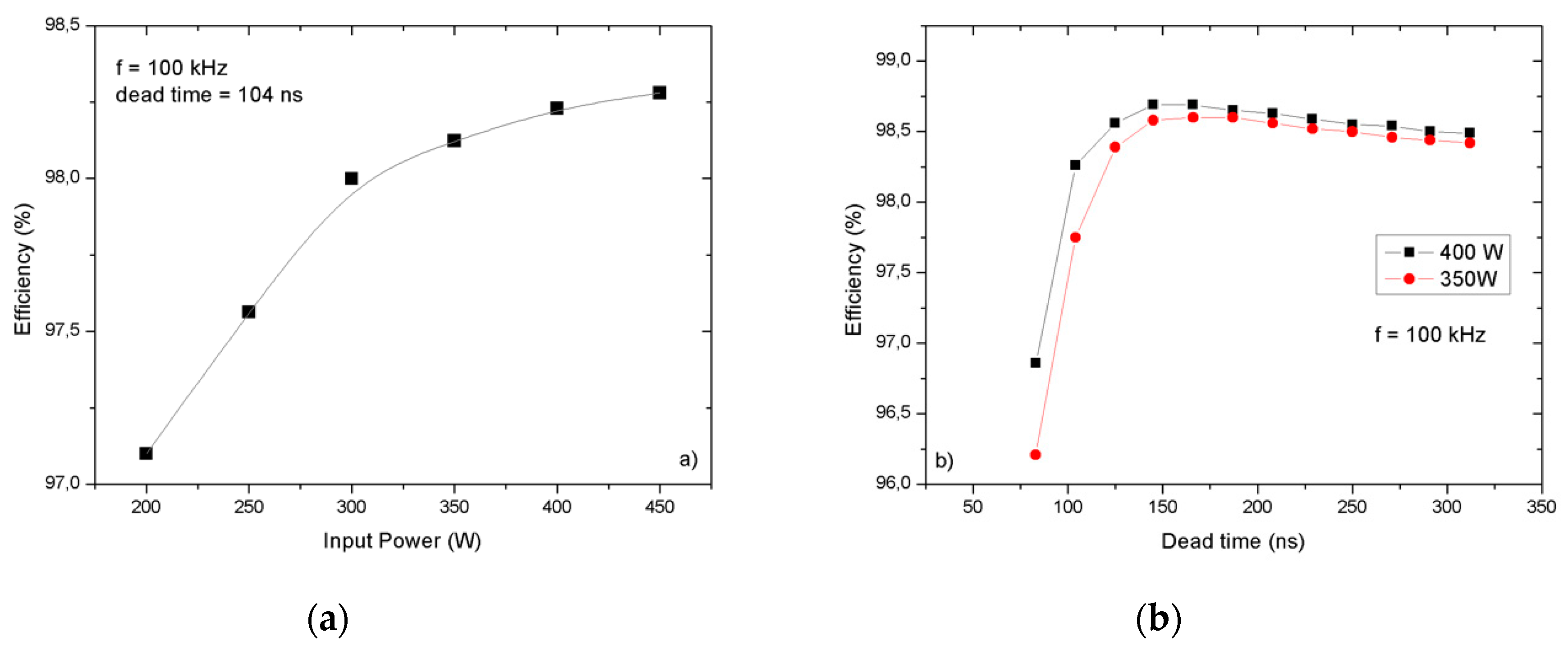
The power shield, using silicon MOSFETs, shows good performances, reported in this document for input powers from 200 up to 450 W.
We considered the power conversion efficiency, defined as .
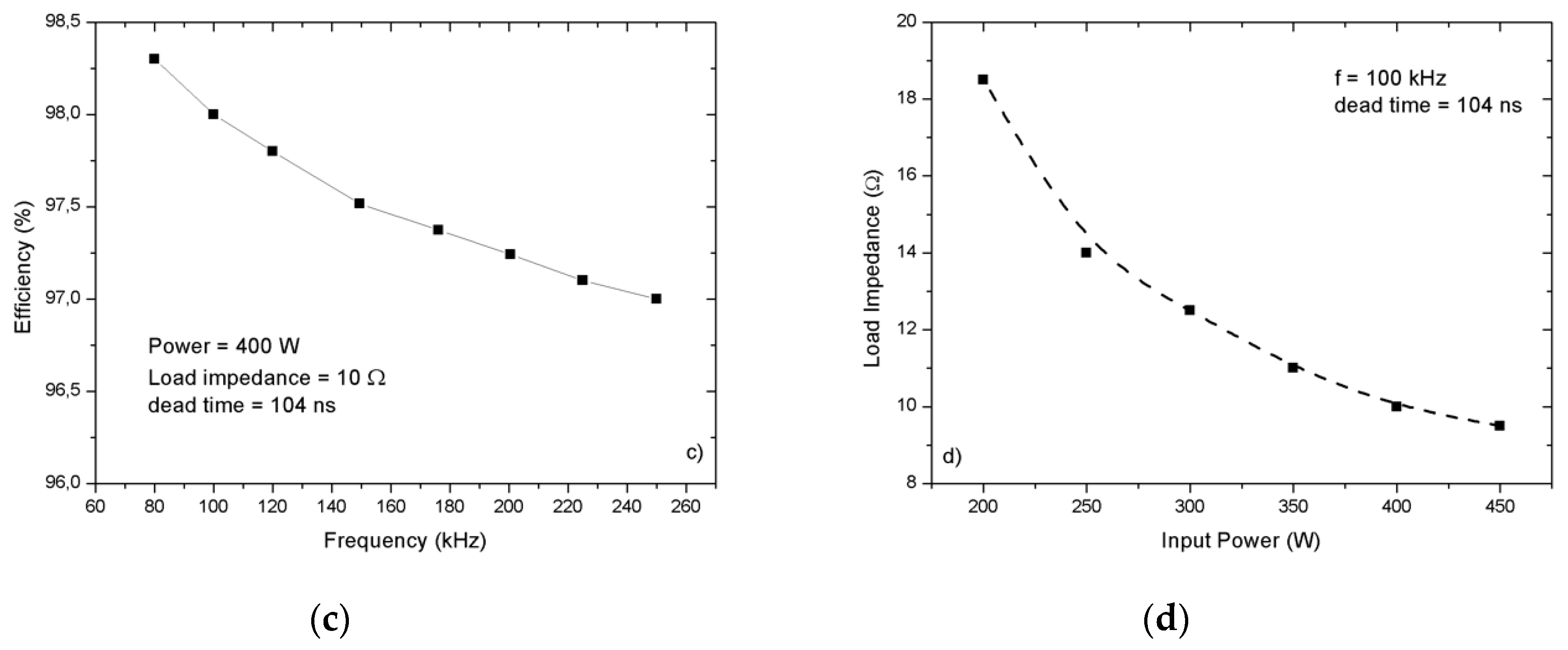
As shown in
Figure 9a, the efficiency (
η) is higher than 97% in the range of considered input powers, higher than 98% for power above 300 W. In
Figure 9b it can be seen how
η presents its maximum value for a dead-time equal to 166 ns, using a switching frequency of 100 kHz, with a maximum value of 98.7% at 400 W of input power.
The efficiency decreases sharply as the switching frequency increase, as reported in
Figure 9c. The measured values of efficiency, reported in
Figure 9, are considered using the measured optimal load impedance, for every input power, detailed in
Figure 9d. The operation of the DC/DC converter in bypass mode shows an efficiency higher than 99%.
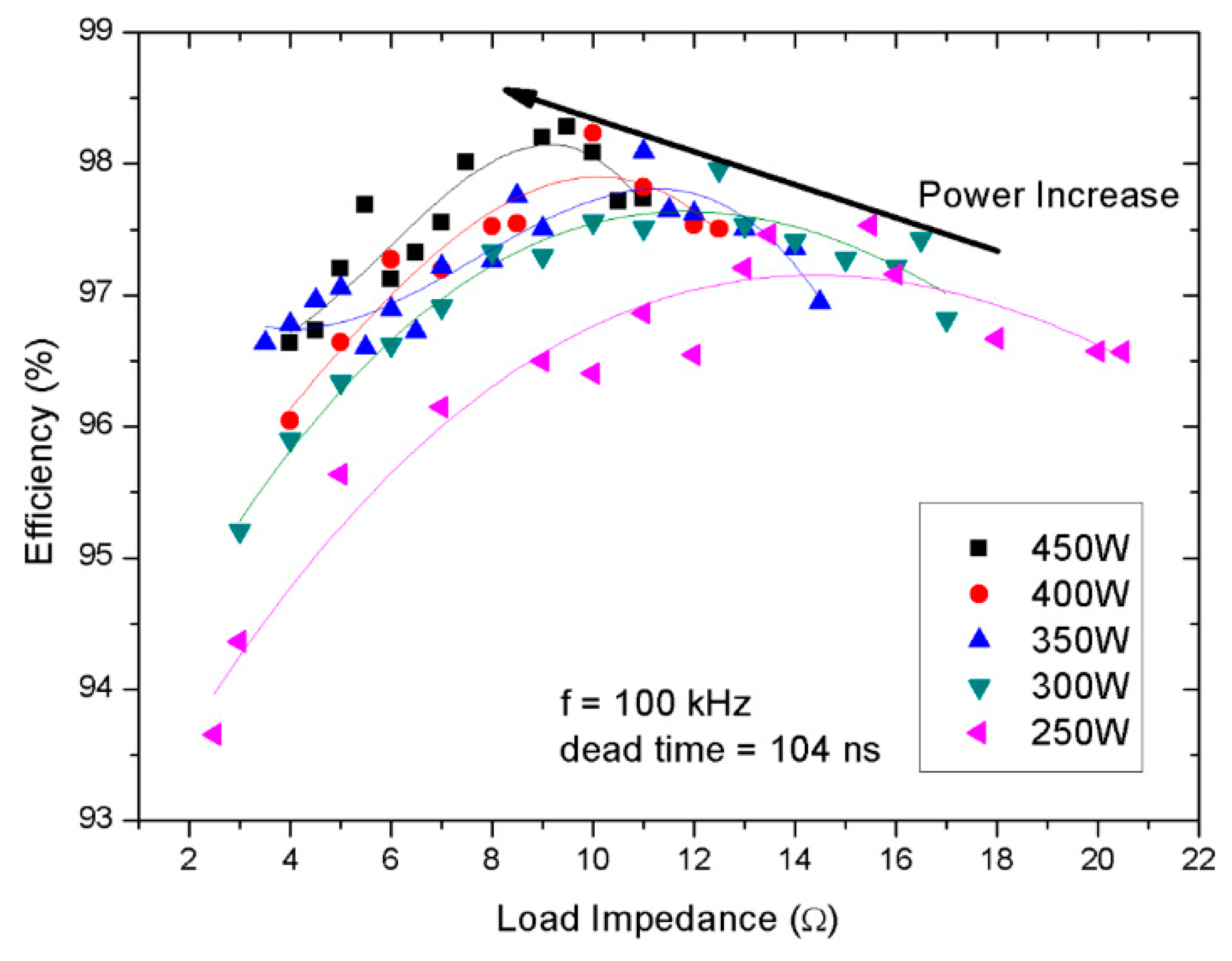
The
Figure 10 reports the curve fitting of the measured efficiency values in the 250–450 W range of input powers, for 50 W step. The optimal value, i.e., the maximum value of every single curve, moves to a lower value of load impedance as a response to the increment of the input power.
6. Discussion
The designed solution is characterized by limits in terms of maximum current, voltage, and power that could be applied to the circuit.
Nevertheless, the overcome of the actual limits is possible but it has the huge drawback of the rapid increase of the bill of material (BOM) cost of the boards, thus reducing the adopting rate from contributors.
Being the repository enabled to host forks of the system, authors welcome contribution that, considering different technological limits and power ranges, could enable the use of a modified version of the system with other renewable energies as, for example, fuel cells.
The actual limits of the platform are a maximum power of 450 W, maximum input, and output voltage of 70 V, 10 A not simultaneously. The maximum PWM frequency used for feeding the gates of the H-Bridge topology is 250 kHz, the minimum dead time is 83 ns.
The undiscussed, provided value of the community improvements on the discussed open-source platform could rely on, but are not limited to, suggestion and test of different devices. For example, the used MOSFETs are in a quite common package, and could be modified with different part numbers thus exploring the overall effects of the parameter modifications. Both FPGA and μC have pinout compatible alternative parts that may differ in terms of LUTs, memory, and peripherals, and could be considered as possible alternatives to reduce the BOM cost or to explore different functionalities.
Nevertheless, different coding strategies could bring benefits on the FPGA and the microcontroller, increasing, e.g., the PWM frequency beyond the actual limit of 500 kHz, and developing further and efficient algorithm.
The user of the platform should be instructed and informed on the fact that he/she is managing high power, which is potentially dangerous, and he/she should use proper countermeasures to reduce every risk.
In case of working conditions that require the platform to perform close to its power limit of 450 W, a cooler device is recommended to help reduce the switching devices temperatures.
7. Conclusions
In this paper, the design and hardware implementation of a platform for the development of smart converter system have been described in detail. The system is conceived as an open-source hardware platform. Schematics, layout, bill of materials, and software programming codes are provided under the terms and conditions of the creative commons attribution (CC BY) license for hardware and MIT license for software.
The proposed system was simulated and constructed, and the functionalities of the suggested control algorithms P&O were proven and discussed. From the results acquired during the hardware experiments, the feasibility and functionality of the platform that allows for the implementation of MPPT algorithms and permits one to achieve an acceptable efficiency level have been confirmed.
A bi-directional radio frequency communication channel using Wi-Fi protocol enables the real-time reading of measurements and parameters, the remote modification of both algorithms type and settings, and the remote diagnostic of the board.
To our knowledge, this project remains the only open-source hardware platform for smart converter development used for educational, research, and industrial purposes so far.
In addition, it is conceived in a flexible and extensible manner so permitting further development for recent energetic scenarios.

 ,
, 


