Control Strategies of Mitigating Dead-time Effect on Power Converters: An Overview


1
Department of Electrical Engineering, Yanshan University, Qinhuangdao 066004, China
2
Department of Energy Technology, Aalborg University, 6700 Esbjerg, Denmark
*
Author to whom correspondence should be addressed.
Electronics 2019, 8(2), 196; https://doi.org/10.3390/electronics8020196
Submission received: 24 December 2018
/
Revised: 22 January 2019
/
Accepted: 26 January 2019
/
Published: 8 February 2019
(This article belongs to the Special Issue Applications of Power Electronics)
Abstract
:To prevent short-circuits between the upper and lower switches of power converters from over-current protection, the dead time is mandatory in the switching gating signal for voltage source converters. However, this results in many negative effects on system operations, such as output voltage and current distortions (e.g., increased level of fifth and seventh harmonics), zero-current-clamping phenomenon, and output fundamental-frequency voltage reduction. Many solutions have been presented to cope with this problem. First, the dead-time effect is analyzed by taking into account factors such as the zero-clamping phenomenon, voltage drops on diodes and transistors, and the parameters of inverter loads, as well as the parasitic nature of semiconductor switches. Second, the state-of-the-art dead-time compensation algorithms are presented in this paper. Third, the advantages and disadvantages of existing algorithms are discussed, together with the future trends of dead-time compensation algorithms. This article provides a complete scenario of dead-time compensation with control strategies for voltage source converters for researchers to identify suitable solutions based on demand and application.
1. Introduction
Power converters are widely used in industrial applications, such as photovoltaic (PV) power systems [1], adjustable speed drive systems [2], and wind energy systems [3]. With the development of power electronics technology and switching power devices, more advanced converters are receiving widespread attention. A dual output single-phase current source inverter has been proposed for microgrid applications. It utilizes six switches to handle power flows to two independent loads with the same or different voltage ratings [4]. The interaction of the cyber twin model by a cyber integration layer with the physical device is needed for effective control of the system. The interest in grid-tied PV transformer-less inverters has increased rapidly because of their higher efficiency and lower cost compared to traditional line transformer inverters. Some new transformer-less have been proposed such as ESI [5], CH5 [6]. The results show that the novel topologies change the common-mode behavior, which consequently allows a significant reduction of ground leakage current. On the other hand, the high-frequency-based medium voltage inverters are used in renewable energy. However, the power quality is compromised as a result of the increase in common mode noise currents by the high inter-winding parasitic capacitance in high-frequency link transformers. To solve this problem, the modified design of a toroid ferrite core transformer offers more resistance to temperature increases without the use of any cooling agent or external circuitry power sources for power transmission [7].
In practice, the power switches (e.g., Insulated Gate Bipolar Transistor (IGBT)) of the voltage source converter have non-ideal features, such as rising and falling time. In order to avoid short circuits of power switches, the dead time is mandatory for operating voltage source converters [8,9], that is, a dead time is set between the driving signals of the upper and lower switches on each bridge arm. In the case of a single pulse, the dead-time effect is not obvious in a speed control system with a low carrier frequency and low performance requirement. However, the dead-time effect in one cycle has a cumulative effect. When the converter operates at low speed and high switching frequency, the accumulated dead-time effect will cause the voltage and current to contain a large number of harmonic components, and will generate a zero-current-clamping phenomenon. The greater the switching frequency is, the more adverse this phenomenon is. Moreover, in the case of frequency conversion, the speed regulation and dead-time effect causes the motor to generate a large pulsating torque and additional loss. Therefore, the dead-time compensation is one of the most important issues for power converters.
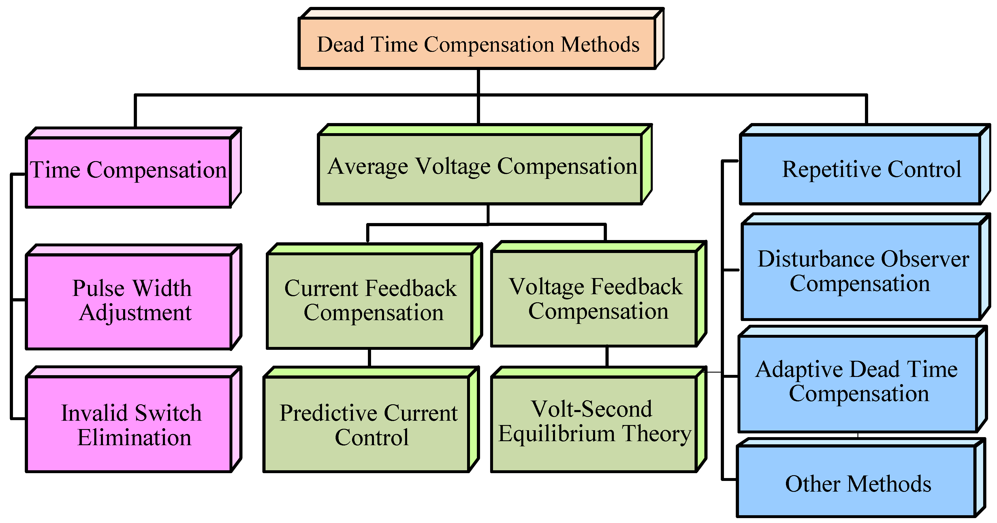
There are two kinds of algorithms for dead-time compensation. One compensates by both software and hardware. The hardware detection circuit is used to judge whether the anti-parallel diode is turned on for the current direction detection. The compensated voltage signal is obtained by comparing the actual voltage and voltage reference. Software is used for the compensation algorithm. The major limitation of this method is that the reliability of the hardware detection circuit cannot be guaranteed, and the complexity of the system is increased. The other method is to simply use the software compensation algorithms only. This kind of method does not require a hardware detection circuit, and is simple and flexible for practical implementations. The classification of the dead-time compensation methods is shown in Figure 1. In general, dead-time compensation methods are divided into three methods: time compensation method; average voltage compensation method; and other methods, which use existing mature modulation technologies. Among these, the time compensation method is most widely used, with other methods using closed loop control.
The remainder of the paper is organized as follows. First, the dead-time effects on the harmonics of the output voltage are elaborated. Second, the different dead-time compensation methods are classified and summarized in detail, and the advantages and disadvantages of various methods are discussed.
2. Dead-time Effect Analysis
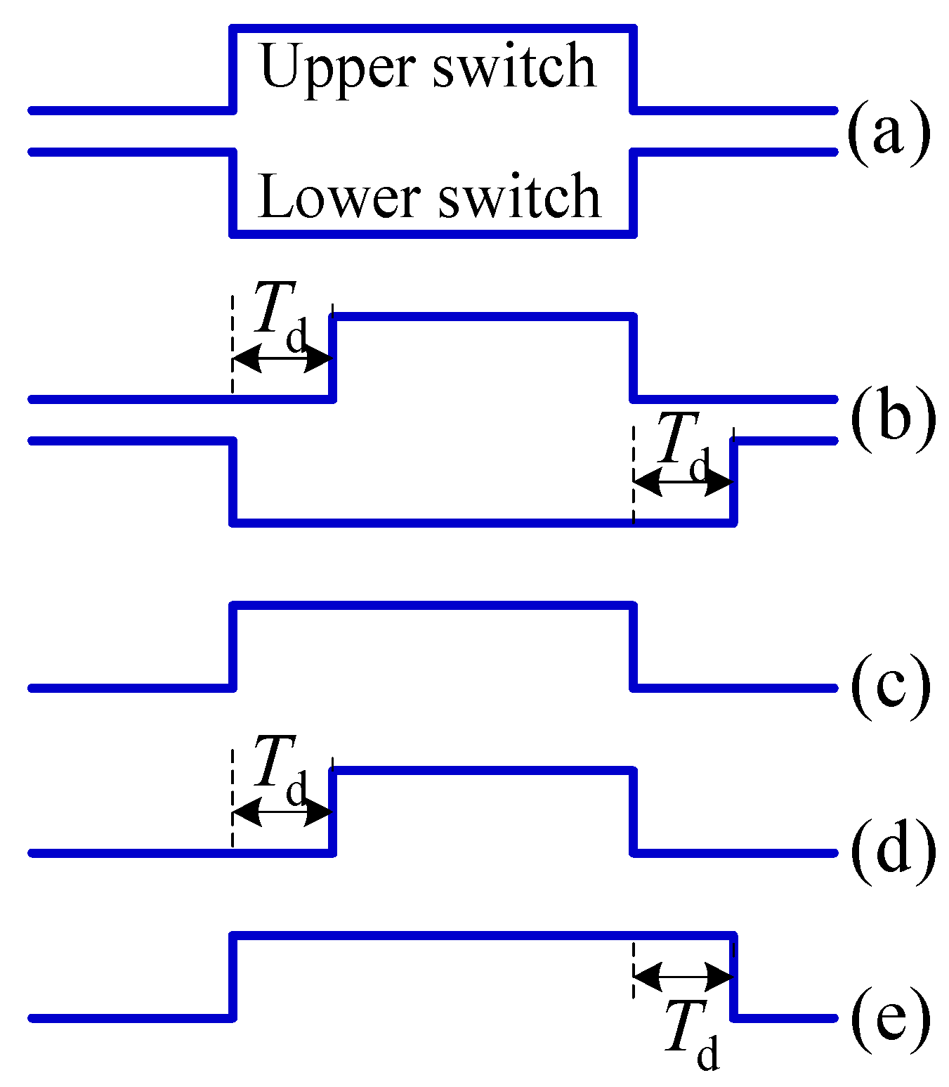
In practice, there are voltage source converters [10] and current source converters [11]. The former is the main topic of this paper. Assuming that when the current flows into the grid, the direction is positive, the driving signal waveform and output voltage waveform of the power switch are shown in Figure 2. The elements of Figure 2 are as follows:
Figure 2a is the waveform of the switch driving signal in the ideal state without dead time.
Figure 2b is the waveform of the switch driving signal with a dead-time state.
Figure 2c is the ideal waveform of the output voltage.
Figure 2d is the actual waveform of the output voltage when i > 0.
Figure 2e is the actual waveform of the output voltage when i < 0.
Figure 3 takes phase A as an example to analyze the effect of dead time on the output voltage and current.
2.1. Effect of Dead Time on Output Voltage
From Figure 2, it is clear that there is an error between the actual and ideal values of the output voltage. The error voltage of phase A can be obtained as follows, where Td is the dead-time, and fc is the switching frequency:
Three-phase phase voltage errors can be analyzed from the Fourier series point of view, as shown in Equation (2), where n = 1, 3, 5, 7, 11, 13, …, and ω is the angular frequency of the output voltage.
The output voltage of phase A by taking the dead-time effect into account can be expressed as:
where M is the modulation index and φ is the power factor angle. The harmonic voltage amplitude decreases as the harmonic order rises. The higher harmonics can be filtered by a low-pass filter, while the low-order harmonics are difficult to attenuate and result in undesirable voltage distortion.
2.2. Zero-Current-Clamping Phenomenon Caused by Dead Time
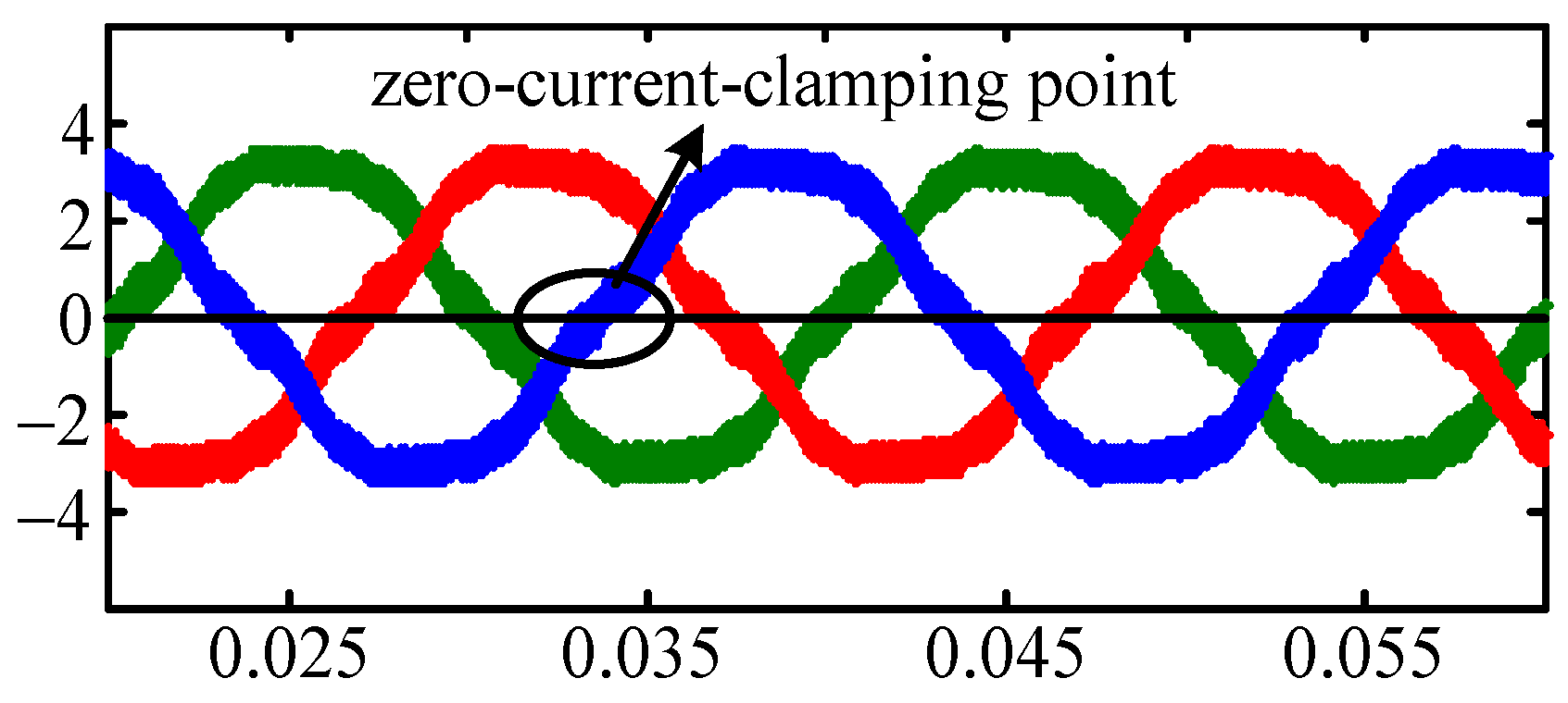
Zero-current clamping means that the current is close to zero in any direction during dead time. Due to the freewheeling action of the freewheeling diode, the current magnitude decreases. When the magnitude of the current is near zero, the dead time begins. Then, when the current drops to zero, the reverse voltage on the diode will prevent the reverse increase of the current, which keeps the current near zero during the remaining dead time. When the output voltage is almost zero, the zero-current-clamping phenomenon causes current distortion and torque ripples. Henceforth, dead-time compensation becomes mandatory for voltage source converters.
Figure 4 is a schematic diagram of zero-current clamping of a voltage source inverter. From Figure 4, the following conclusions can be drawn as follows:
- (1)
- The zero-current clamping of the inverter dead time occurs near the current zero crossing, and the current is clamped near zero during the entire dead time.
- (2)
- The current is little affected by the dead time for a period of time before zero crossing, and it is clamped to near zero for a period of time after zero crossing.
Therefore, during the period of zero-current clamping, it is inaccurate to compensate the voltage error by judging the current direction based on the current only.
3. Dead Time Compensation Methods
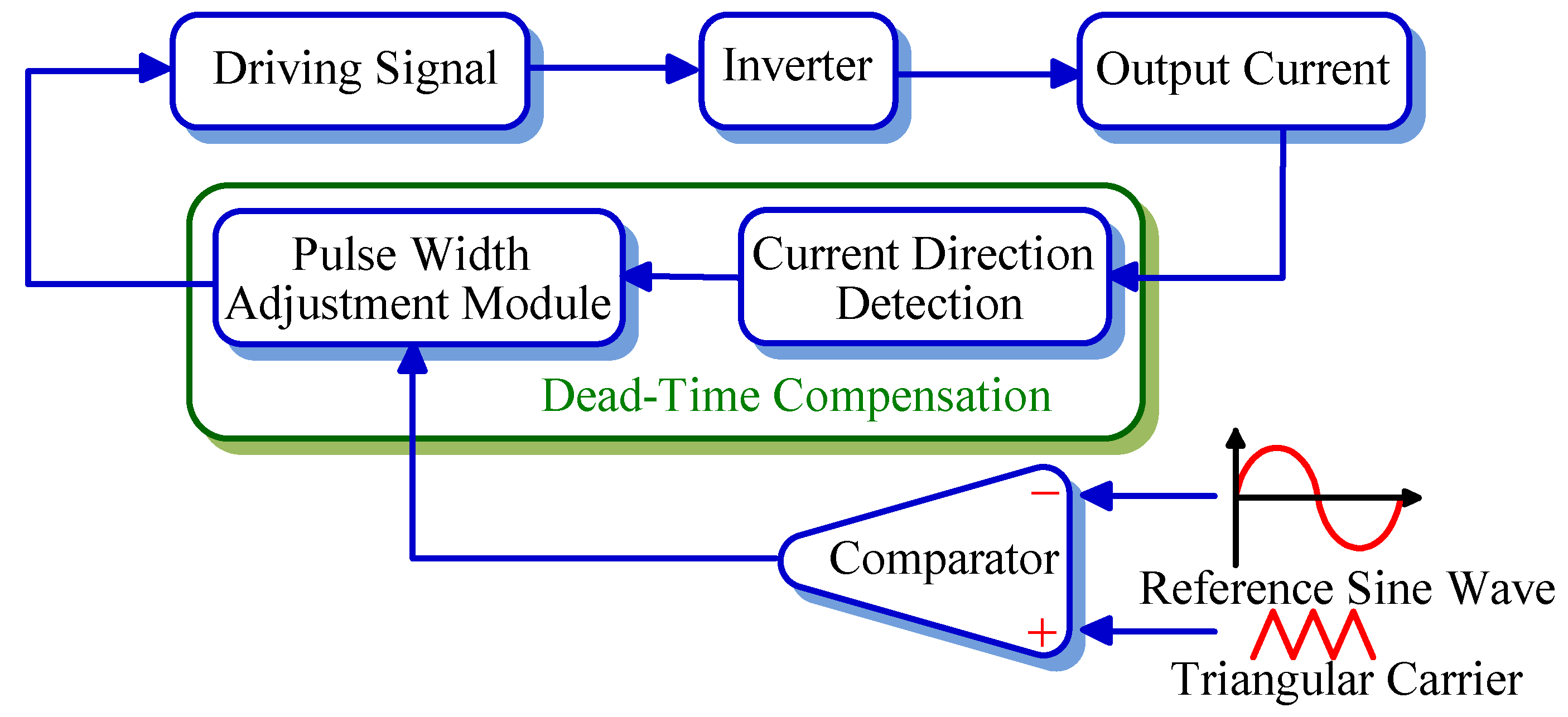
3.1. Pulse Width Adjustment Method
The pulse-width adjustment method (also named the time compensation method) changes the pulse-width by lagging or leading the turn-on or turn-off time of the power device according to the dead-time insertion, so as to compensate for the effect of dead time [12,13]. It requires the direct adjustment of real-time pulse-width in each switching cycle. Therefore, it is relatively complex to implement. Figure 5 is a schematic diagram of the pulse-width adjustment method, where the dead-time compensation method based on pulse-width adjusts to ensure that the output voltage waveform is the same as the ideal waveform.
In order to solve the problems of phase voltage and phase current distortion and zero-current clamping caused by dead time, a novel adaptive dead-time compensation strategy is proposed in [14]. The strategy does not require current polarity detection. In the synchronous rotating coordinate system, the observed q-axis disturbance voltage is adjusted by a proportional integral (PI) controller to obtain the dead-time compensation time. The dead-time compensation time is allocated according to the ratio of the action time of the two non-zero space voltage vectors.
A tri-carrier Sinusoidal Pulse-Width Modulation (SPWM) used to eliminate dead-time effects is proposed in [15]. It directly modifies the modulation strategy to remove dead-time. It also can reduce current harmonics and suppress the current ripple on the AC side of voltage source converters. Triple carriers are used to modulate the modulating wave. According to the current direction after filtering, the driving signals are obtained by simple logic operations. This method can improve the performance of the induction motor (IM).
A dead-time compensation scheme is presented for a six-switch three-phase output inverter in [16]. The error is compensated by extension or reduction of the switching conduction period. The extended object, which is a turn-on or turn-off period for each switch, is varied by the direction and the magnitude relationship of the output current in each phase.
In order to simplify the time compensation algorithm, a method for measuring the narrow pulse width of a pulse train through a single-channel time analyzer is reported in [17]. This provides no limit to the dead time of the measurement channel. Simultaneously to the periodic jitter measurement of the pulse train, it can estimate both pulse-width measurement error and minimum pulse width, which is determined by specifying a relative measurement error.
Furthermore, the dead-time compensation method presented in [18] reduces the delay time and minimum pulse width. Therefore, it is able to completely compensate for voltage distortion, even if the input signal includes narrow pulses.
In [19], the dead time at the initial stage of the pulse-width modulation (PWM) generation is introduced. The protection algorithm ensures that the two series switches are not conducted at the same time and no switch is turned on during the dead time.
In the voltage source converter, due to the effect of dead time, the fifth and seventh current harmonics are generated in the stationary reference frame, and the corresponding sixth current harmonic is generated in the d-q synchronous reference frame, respectively. A proportional integral (PI) current regulator in the synchronous frame is used to compensate the distortion results from the dead time [20].
A correction strategy of major contributors that causes voltage distortion has been put forward by analyzing and quantifying the contributors [21]. Unlike the previous reported solutions, the contributors to voltage distortion are analyzed and quantified. The duty cycle of each phase is adjusted as a function of current feedback or current command to mitigate the voltage distortion due to switch dynamics.
The effect of dead time of a three-level neutral-point clamp (NPC) voltage source converter is discussed in [22]. The self-balancing space vector pulse-width modulation (SVPWM) is presented to improve the effect of dead-time compensation. It provides a cost-effective pulse-based dead-time compensation for three-level voltage source converters.
The effect of dead-time, as well as minimum and maximum pulse-width effects, on the continuous and discontinuous pulse-width modulations, is discussed in [23]. Considering that the controller is not able to compensate for dead time in the case of minimum pulse-width, two compensation methods are developed. One solution, used for the moderate modulation index, is to switch between DPWM (Discontinuous Pulse-Width Modulation) methods to avoid a distorted region and allows a loss-optimized DPWM method. It is used for the maximum part of the operating time. Another method, used for the high modulation index, is proposed to maintain the linearity of the fundamental voltage component. The above two methods are able to reduce the sixth voltage harmonics.
A new integrated dead-time space vector pulse-width modulation technique is proposed to control a voltage source inverter in [24]. The proposed algorithm is modified to ensure the duty ratios are independent of sampling time T and carrier frequency fc. After the duty ratios are generated by using the modified modulation technique, an integrated dead-time insertion block is used for given T and fc by taking the three-phase duty ratios as inputs.
The fixed dead-time control strategy may lead to unwanted body-diode conduction or momentary cross-conduction. Considering that the optimum dead time varies with the load current, it is important to continuously adjust the dead time in a cycle-by-cycle manner. An improved solution is proposed to predict the optimal dead time and eliminate the cross-conduction and body-diode conduction [25]. It is able to adjust the optimum timing for both the rising and falling edges of the output switching waveform for the converter.
In [26], the impact of the dead time on common-mode voltage is discussed. A modified pulse-width modulation method is presented to eliminate common-mode voltage due to the dead-time effect. Another dead-time compensation method superimposes the square wave on the triangle wave [27]. The triangle carrier and the square wave have the same frequency. The amplitude of the square wave is equal to that of the dead time. It is simple to implement in practice. Based on a back calculation of the current phase angle, a new on-line dead-time compensation method is proposed in [28]. A detailed switching characterization with dead-time effect in all operation states is discussed in [29]. A dead-time compensation method for a three-level voltage-source inverter is proposed in [30]. It is based on the fact that the voltage error caused by dead time depends on current polarity, and inserts the dead time at the instant of turning on and off of switches. The algorithm is simple and eliminates current harmonics.
It can be concluded from the above that the advantage of the pulse-width adjustment method are that the compensation accuracy is high, the voltage is compensated and has no error, and the compensation method is only related to the polarity of the current. It is simple and intuitive, and has good real-time performance. However, the pulse-width is simultaneously directly adjusted during each switching cycle, which occupies a large amount of computing resources of the controller, and the ambiguity of the zero-crossing point of the current affects the accuracy of the compensation.
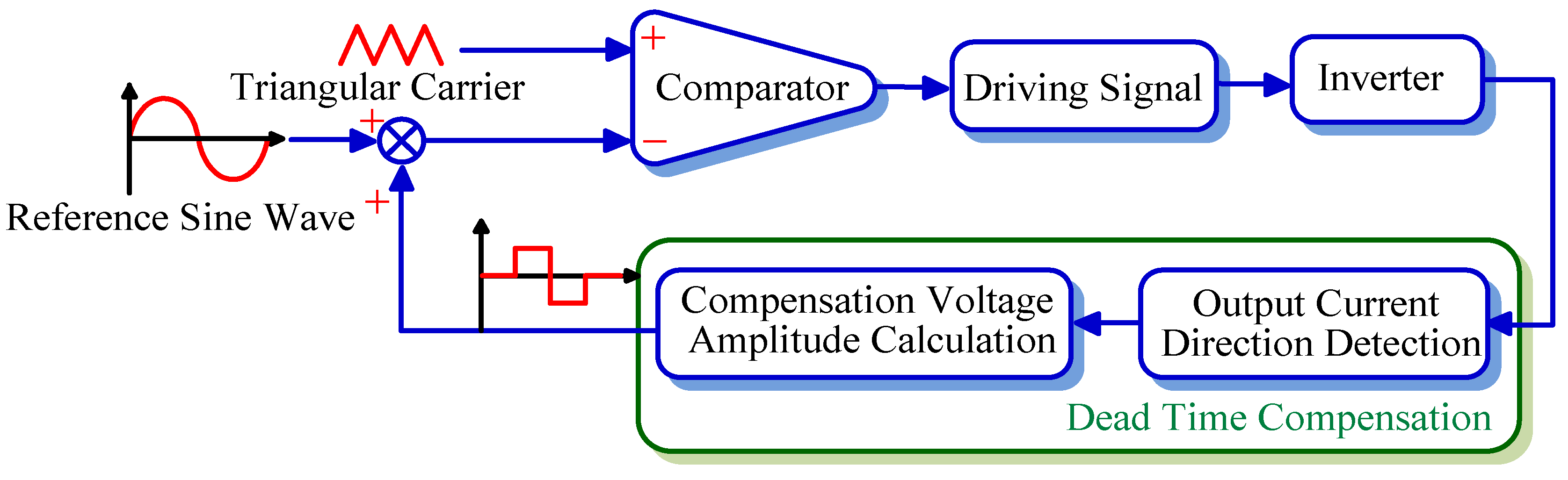
3.2. Average Voltage Compensation Method
The average voltage compensation method averages the deviation voltage that is caused by the difference between the output voltage and ideal output voltage waveform [31]. Dead-time compensation is completed by feeding forward the averaged deviation voltage. Compared with the pulse-width adjustment method, it is much simpler. Figure 6 shows a schematic of the average voltage compensation technique and elaborates in detail.
The direction of the output current of the converter is sgn(ia):
The dead-time voltage required for each modulation period in bipolar modulation is:
where Ts is the switching period, Vdc is the DC voltage and td is the dead-time.
The compensated voltage Utdm superimposed on the modulating wave voltage and compared with the carrier to obtain a PWM driving signal. This kind of method has the same issues as the pulse-width adjustment method, such as compensation error around the zero-crossing region. The major reason for this is that the compensation voltage is determined by the current detection signal. Therefore, the accuracy of current detection directly affects the compensation accuracy.
In order to minimize the harmonic current distortion caused by dead time, a simple dead-time compensation technique is proposed in [32]. With a suitable PI current controller, the proposed technique easily be added into the synchronous reference frame current (cf. d-q axis) control. With the proposed technique, the output of the PI current controllers can be limited to lower values to reduce an integral windup problem and improve control capability of the system.
A new dead-time elimination method is proposed in [33]. It uses a low voltage detector circuit connected in parallel to each device to measure the terminal voltage of power switches. It can reduce voltage distortion.
An accurate compensation based on the average-value theory is presented in [34]. The compensation factor is adjusted according to the accumulated error within a half period of the output current. The proposed method evaluates initial compensation voltage according to the dead-time and switching cycle, and a proportional factor is introduced to the compensation voltage. The exact compensation factor is obtained by minimizing the harmonic component of the current in the synchronous frame. The compensation voltage introduced by the dead-time, turn-on/off delay and voltage drop across the power switches can be accurately identified by the proposed method. Another method based on the virtual inductor is proposed for dead-time compensation in [35]. It is able to reduce current distortion. Another improved compensation based on the average error voltage is proposed in [36]. Different from conventional methods, which have amplitude and phase errors at the output voltage, it can achieve dead-time compensation with much less amplitude and phase errors. A new distortion voltage compensation method for eliminating the effect of dead-time on zero-current clamping is proposed in [37]. The modeling analysis of the dead-time effects on parallel converters is discussed in [38]. It is useful to evaluate the impact of dead-time on the circulating current of voltage-source converters.
In summary, the average voltage compensation method is simple and convenient, easy to implement, and feasible. However, the zero-crossing detection accuracy is not high enough, and error compensation will occur, causing new harmonics in the output voltage and current.
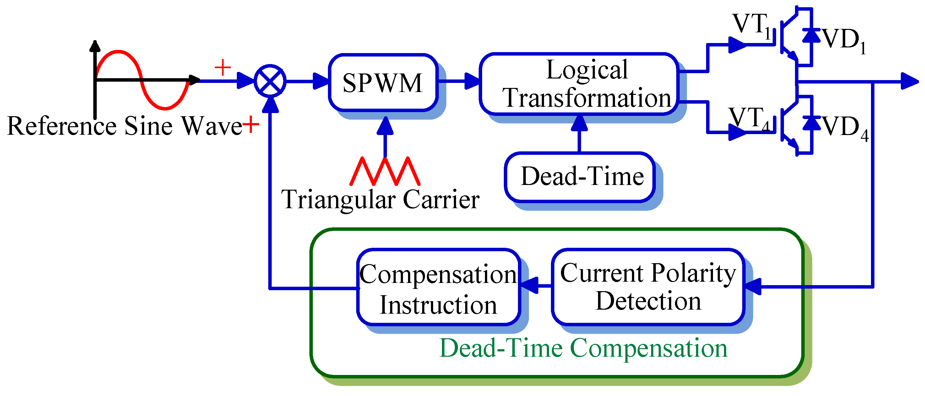
3.3. Current Feedback Method
The current feedback dead-time compensation method determines the compensation voltage by detecting the polarity of the output current of the converter [39]; a schematic diagram is shown in Figure 7. In practice, it is affected by the dead-time, amplitude and frequency of the current. Actually, the zero crossing of the current is not easy to detect. Moreover, the necessary current filters also exacerbate the difficulty of detection of the current polarity, especially when this method is implemented in software. Severe detection delay will destroy the correct compensation of dead-time.
The current feedback needs to detect the polarity of the phase current and convert the polarity of the current into a square wave voltage, which is added to the modulation wave of each phase. This square wave voltage causes the inverter to generate a current phase that is the same as the error of the compensation voltage. Generally, in the control system, there are three kinds of methods used to detect the polarity of the current:
A. Direct detection of current zero-crossing point
This method determines the modulation plus or minus compensation voltage according to the current sign. Its key characteristic is its simplicity, but it needs to accurately detect the current zero-crossing point, especially when the frequency is relatively low, or else it will lead to incorrect compensation because the current zero-crossing point is not obvious.
B. Prediction of zero-crossing point
This method is an improvement of method (A), realizing the advance detection of the current zero-crossing point, which is usually used for high-frequency bands. It has a good compensation effect.
C. Dead-time compensation based on rotor magnetic field orientation
The method performs coordinate transformation on the three-phase output current, then calculates the current vector angle according to the synchronous rotation angle of the rotor field orientation, and finally compensates for the dead time according to the current vector angle. Usually, the three-phase output current pulse has a better compensation effect.
Figure 7 shows a schematic of current feedback compensation. It is known that, due to the influence of dead-time, the output current contains harmonics. A method named the current harmonic filter method calculates the compensation voltage by filtering the sixth current harmonic in the d-q synchronous rotating coordinate system [40,41]. The output current of the grid-tied inverter contains odd-numbered harmonics because of dead-time and nonlinear characteristics of the switching devices. A new compensation algorithm using the second-order generalized integrator (SOGI) is proposed to reduce the dead-time effect [42]. By using synchronous reference frame, even-harmonic components are generated by the dead-time effect. Accordingly, SOGI detects the specific frequency used to reduce the dead-time effect. This algorithm does not require any additional hardware or other information, except phase current and grid angle information. The output current harmonics are effectively eliminated by controlling the error terms of d-q axis currents.
A novel method of compensating for dead-time effects, which uses a feed-forward approach for the standard compensation and a feedback loop with adaptive harmonic compensator to suppress the persistent sixth harmonic components in the d-q axis current, is presented in [40]. This method does not rely on parameter calculation.
In [41], a novel online dead-time compensation strategy for a vector controlled permanent-magnet synchronous motor (PMSM) is proposed. The output of the adaptive method is a slowly time-varying voltage, which is used to compensate for output voltage distortion. Although the current harmonic filtering method does not depend on current polarity detection and motor parameters, it is affected by the zero-current-clamping phenomenon.
In a voltage source converter, the dead-time effect can be divided into the controlling dead-time effect and switching dead-time effect. The switching dead-time effect includes the turn-on and turn-off time delay of the power devices, the voltage drop of the power devices, and the influence of parasitic capacitance. In order to reduce the switching dead-time effect, a dead-time compensation method to reduce the influence of zero-current-clamping and parasitic capacitance has been raised [43]. The method is used to calculate the three-phase compensation voltage according to the polarity of the three-phase current and the compensation time, and to correct the error polarity of the compensation voltage caused by the zero-current-clamping phenomenon. Since the magnitude of the compensation voltage varies with the current, this method has the disadvantage that the reference quantity is the amount of change when the voltage polarity is corrected.
The polarity of the current is often difficult to determine accurately, mainly because the accuracy of the current detection is affected by the dead-time, amplitude and frequency of the current, thus the output current of the converter is distorted in the zero region and the current zero-crossing point is more difficult to determine.
The dead-time effect is created by using the change of the slope of the current waveform caused by dead time to compensate for the deviation voltage [44], but this method relies on the correct judgment of the polarity of the current. If the polarity is judged incorrectly, it will lead to a worse compensation effect.
In order to reduce the voltage error and current waveform distortion caused by dead time, current feedback control is applied to a three-phase power factor correction rectifier and power device ripple filter with a small capacitance value using a high feedback coefficient [45]. Since the small capacitor on the AC side easily leads to system instability under a high feedback coefficient [46], this method cannot effectively suppress the current ripple due to dead time.
A method compensating for dead-time harmonics by including a harmonic compensator with a current controller is proposed in [47]. A multiple-parallel resonant controller is adopted, which enables selectively canceling out the harmonic components or a repetitive controller mitigates all harmonics below the Nyquist frequency.
For the well-known problem of determining the current polarity in the zero-crossing region of the current, a solution to minimize the voltage distortion in the zero-crossing region is discussed [48]. In the proposed solution, the polarity of the current and its instantaneous value is employed to correct the pulse-width. The experimental results show that the compensating term is maintained at a fixed value no matter the polarity and magnitude of the current flowing through the power switch.
For the problem of a low current with multiple zero-crossing points during a switching period, a new method which uses a model for calculating the voltage error caused by dead time has been put forward [49]. This determines the dwell time and integrates the volt-seconds for a half period of the triangular carrier. Each half period of the triangular carrier split to time segments. The resulting error voltage is used to calculate a new compensated duty factor. Another method that uses the model to calculate the deviation voltage caused by dead time is introduced in [50]. It uses a model to split each half period of the triangular carrier into time segments where the slopes of the currents in all phases and the output voltage of all semiconductor phase legs are constant. It determines the duration of each time segment and integrates the voltage-seconds for a half period of the triangular carrier. The resulting error voltage can be used to calculate a new duty cycle to compensate for dead time.
As is known, the amplitude of the square wave modulated by SPWM is basically constant, and the amplitude can be estimated without additional hardware. The structure is simple, easy to implement, and has a practical application value. On the other hand, the compensation effect is greatly affected by the current detection accuracy, and accuracy of the zero-crossing point of the current detection becomes the decisive factor in determining the compensation effect.
3.4. Voltage Feedback Method
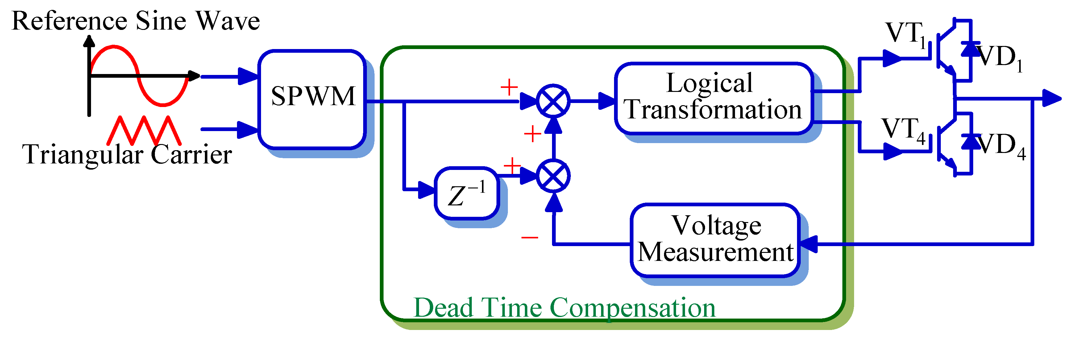
The voltage feedback dead-time compensation method compares the actual output voltage of each phase with the reference output voltage to obtain the deviation voltage, and superimposes the deviation voltage with the reference voltage to obtain a new reference voltage [51]. Because each comparison must be corrected at the next switching cycle and the output voltage must be accurately detected, this method also has hysteresis and is complicated to implement. Figure 8 shows a schematic of voltage feedback compensation.
The error voltage vector caused by the dead-time effect of the PWM inverter is given by [52]. Using the vector synthesis method, the formulae for calculating the amplitude and phase of the composite voltage vector are deduced, and the characteristics of the composite voltage vector are analyzed by simulation. In order to ensure that the actual opening time of the switch tube is equal to the ideal given opening time, a dead-time compensation method is proposed. Combined with the characteristics of SVPWM, a simplified formula is obtained. In order to eliminate the error voltage vector, a dead-time voltage compensation method is proposed. According to the difference between SPWM and SVPWM, the equations for dead-time voltage compensation in the stator three-phase stationary frame and the two-phase stationary frame are calculated separately. The experimental results show that the proposed compensation method can improve the output performance of the inverter.
In some control strategies, it is necessary to use the output voltage to calculate some state values, but it is difficult to accurately measure the output voltage of the converter. Therefore, the reference voltage is often used in place of the actual output voltage. However, due to the effect of the dead time of the power devices, the output voltage is distorted, resulting in inconsistency with the reference voltage. Therefore, the reference voltage is used instead of the output voltage after compensating the output voltage [53].
The classical dead-time compensation scheme is to add an extra voltage command to counteract the voltage error using a similar approach. The compensation signal is generated based on the precise analytical voltage. The voltage deviation can be compensated by adjusting pulse-width accordingly.
According to the current feedback compensation methods, the distortion of the output voltage results in the generation of fifth and seventh harmonics in the current of the stationary coordinate system, and the generation of the sixth harmonic in the current of the synchronous rotating coordinate system. Various harmonic attenuation methods are proposed [54,55,56,57,58]. The output signal of the PI current regulator in the synchronous coordinate system, which is used to compensate for voltage distortion, is selected and processed in [59]. This method reduces voltage distortion by compensating the d-axis output voltage and the q-axis current regulator.
It is known that the deviation voltage is directly detected, and that the error caused by the dead-time effect can be eliminated and is not affected by the change of the load current. This structure is complicated, and an additional voltage detecting circuit is needed. The small dead-time value requires real-time and accurate detection.
3.5. Adaptive Dead-Time Compensation Method
During processing and analysis, the adaptive control method automatically adjusts the processing method, sequence, parameters, boundary conditions, or constraint conditions to adapt to the statistical distribution characteristics and structural characteristics of the processed data to obtain the best treatment effect.
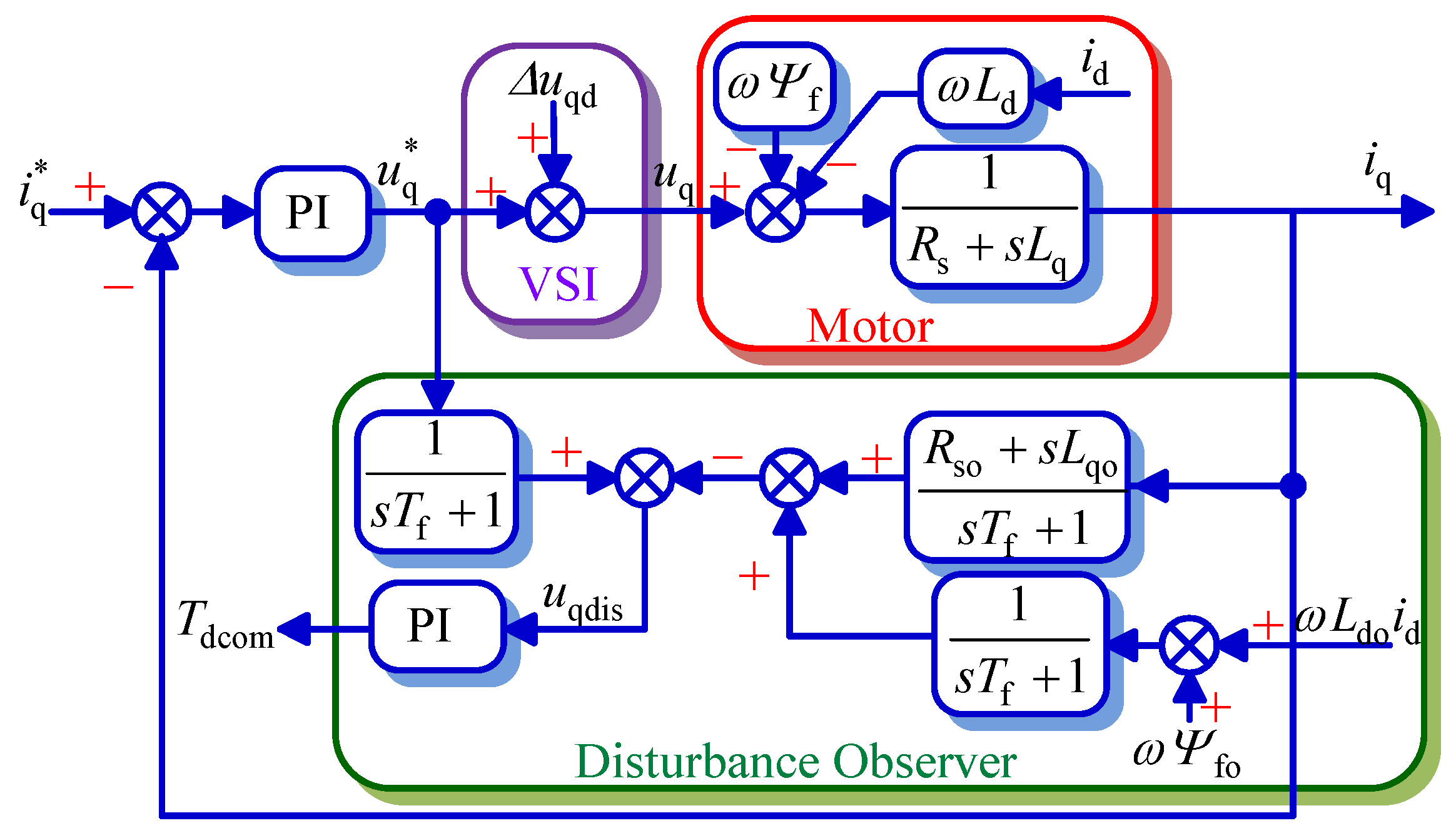
An adaptive observer-based method, which does not require current polarity detection, is brought forward in [14]. This method uses the PI controller to adjust the q-axis disturbance voltage observed in the synchronous rotating coordinate system to obtain the compensation time of dead time. On the basis of conventional SVPWM [60], in each sector, the compensation time is allocated according to the ratio of the dwell time of the two non-zero space voltage vectors. Finally, the dwell times of the two vectors, respectively, are compensated by the allocated compensation time. An adaptive estimation principle diagram of compensation time based on disturbance observer is shown in Figure 9, where PI is the proportional integral controller, uqdis is the q-axis disturbance from the disturbance observer. The compensation time is obtained by the disturbance and the PI regulator.
The conventional sliding mode observer (SMO) collects the rotor position angle by identifying rotor position angle, and needs to introduce a phase-locked loop (PLL) to realize the reverse control. It has certain limitations, including massive calculation, slow dynamic response and complex methods, and not taking the effect from the inverter dead time on the estimation model into consideration during the identifying process. To solve the problems, a new sensorless control method for the adaptive SMO based on a rotating coordinate system and considering dead-time has been proposed [61]. Based on the conventional hypothetical rotational co-ordination system approach, and combined with the model motor approach, this method takes the rotation speed of the hypothetical coordination system as a controlled variable and improves the response speed. Meanwhile, the voltage change triggered by the inverter’s dead time is taken into consideration and the motor current control is achieved through the SMO, which reduces the error between the model and actual motor current to be zero. This method can be realized easily and achieves the motor’s positive-negative rotation control.
A dead-time optimization technique for a two-level voltage source converter using turn-off transition monitoring is proposed in [62]. By tracking the change of the load on-line, the method can adaptively calculate the optimum width of the inductor current zero-crossing region to eliminate the dead-time effect of the zero-crossing region and the non-zero-crossing region, respectively. This technique can effectively eliminate dead time regardless of the load during the entire modulation period. This method not only reduces the output voltage’s fundamental distortion and low harmonic content, but also introduces the adaptive algorithm, greatly reducing the accuracy requirements of the current sampling device and effectively improving the practicality of the dead-time elimination method and the reliability of system.
In [63], an adaptive dead-time compensation strategy to obtain fundamental phase voltage for inverter-fed vector-controlled PMSM drives proposed. A phase dead-time compensation voltage (DTCV), which is used to compensate for the disturbance voltage, is transformed into q-axis DTCV in the rotor reference frame. The relationship between dead-time compensation time (DTCT) and the q-axis DTCV, when the d-axis current is zero, is investigated. In this study, the q-axis DTCV is considered to be the same as the q-axis interference voltage. Adaptive DTCT is used to determine the amplitude of the phase DTCV. Since only the amplitude of the phase DTCV is adjusted, this method has less influence on the estimation delay of the disturbance observer.
There is a dead-time problem in the PWM control of the motor, and it seriously affects the performance of the motor. In order to eliminate the influence of noise, an adaptive filtering method has been presented [64]. The response speed of the filter is improved by the dynamic convergence coefficient. Experimental results show that this filtering method is highly suitable for dead-time compensation, which is based on the current vector. Compared with other noise removal methods, the algorithm is concise and easy to program.
Based on the influence of dead time on the PMSM inverter, a dead-time compensation method based on the Kalman filter has been brought forward [65]. This method is used to filter system noise and the generation of fifth and seventh harmonics in the α and β static coordinate frame, so as to obtain the direction of the three-phase current and the error voltage vector reduced by dead time. According to the error voltage vector, the dead-time effect can be suppressed. The experimental results show that the proposed method can effectively improve the output current waveform of the inverter and the performance of the PMSM system.
In [40], an adaptive dead-time compensation method based on sixth harmonic elimination is proposed. In order to improve the performance of the control algorithm, the method uses an adaptive harmonic filter to suppress the sixth harmonic. PI controllers are used in the proposed method. These controllers have appropriate parameters and effectively suppress the sixth harmonic current in the d-q axis.
Aiming at the online dead-time compensation for PMSM, which is controlled by a vector, a new online dead-time compensation strategy has been discussed [41]. The proposed method is composed of two parts. The first independent part of the parameter is an adaptive method based on the monitoring of harmonic distortion in the d-axis current. Therefore, the criterion is defined as the sum of squared direct axis current between the two zero-crossing points of the phase current. The criterion is minimize by the PI controller, and the output of the PI controller is a slowly time-varying voltage, used to calculate the compensation voltage. This method is extended by the constant voltage disturbance observer of the PMSM model.
Some industrial processes are affected by not only different gain and time constants, but also dead-time. For such industrial processes, the present classic self-regulating regulator is not applicable because it needs the time delay of the process.
In order to control the switching time and simultaneously eliminate the power losses caused by body-diode conduction, power-stage shoot-through current and inductor reverse current, an adaptive inverter-based dead-time controller for synchronous DC-DC converter is proposed in [66]. To achieve even faster comparison, an inverter is used to replace the high-speed comparators in the proposed dead-time controller. In addition, a two-step (coarse- and fine-tuning) dynamic delay generator is proposed for accurate switching time and a wider dead-time correction range comparing to the conventional design. Thanks to the novel adaptive dead-time controller, it is able to dynamically adjust the dead-time to its optimal value with a very wide load range.
An adaptive-linear-neuron (ADALINE)-based dead-time compensation method used for vector-controlled PMSM drives is put forward in [67]. Four ADALINEs are employed in the proposed method. Two ADALINEs are used for estimating the sixth-order harmonic components of d-q axes currents, and the other two used for generating the compensation voltages of d-q axes. Without any additional hardware and complicated signal processing algorithms required, the method is easy to implement.
Because of fault tolerance, adaptive dead-time compensation has the ability to adapt to changes in dynamic behavior of controlled objects, parameters and operating conditions. On the other hand, the disadvantage of this method is that simple fuzzy processing of information will lead to reduced control accuracy and dynamic quality of the system, and the design is not systematic and cannot define control objectives.
3.6. Predictive Current Control
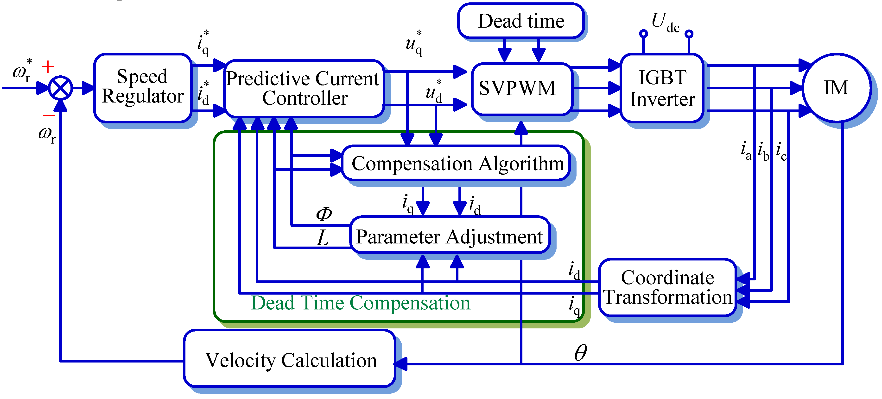
The predictive current control method uses predictive control to control the voltage source converter; that is, to use the known state of the present sampling point, the circuit model, and the reference current of the next sampling point to predict the voltage that can make the output current reach the desired current [68]. This method is implemented only with software. Figure 10 shows the schematic of predictive current control.
In order to improve the adaptability of the system, a novel closed-loop adaptive method is proposed in [69]. The method uses the duty ratio instead of the average deviation voltage, and feeds forward the duty cycle of the compensation time. Simultaneously, the method uses the predictive current controller (PCC) to regulate the phase current. The method is simple to implement, has high computational efficiency, and is easily added to the existing PCC. This method can enhance the dead-time suppression capability of the PCC without modifying the internal structure.
With dead-time compensation, a control method of a doubly-fed induction generator with a three-level midpoint-clamped inverter with dead-time compensation is described in [70]. The principle of the proposed control scheme is to use a dynamic model to predict the voltage value, the rotor current and the DC bus capacitor voltage vector of the next sample point. However, dead time also can cause errors in the established model. Therefore, taking dead time in the model into account, active and reactive power can be estimated based on the stator flux and rotor currents to compensate for dead-time effects. The cost function in this prediction algorithm considers active power, reactive power, and the error between the reference capacitor voltage and the actual. The algorithm selects the optimal switching state of the minimum value function to achieve the purpose of reducing the switching frequency and the common mode voltage.
A predictor structure derived from the filtered Smith predictor is discussed clearly in [71]. The structure is used to simplify the tuning in the robustness of model predictive controllers (MPCs) and improve robustness. The stability and robustness of linear MPCs are analyzed, and this method is extended to nonlinear MPCs of a class of nonlinear systems. The key idea of this method is to separate the predictive structure from the optimization phase in order to guarantee input-to-state stability and constraint satisfaction by using an equivalent dead-time free system.
Although the MPC technique can easily deal with the dead-time effect due to its internal prediction structure, in order to improve robustness an appropriate predictor for the MPC algorithm needs to be defined. A filter-based Smith prediction structure is put forward in [64]. This prediction structure simplifies the traditional prediction algorithm and improves robustness. The key to this method is to separate the predictor structure from the optimization phase so that stability can be guaranteed using an equivalent system without dead time so that the constraints are satisfied.
A predictive method which allows the compensation of dead-time in a Voltage Source Inverter (VSI) feeding an Induction Motor (IM) with the control of SVPWM is discussed in [72]. Based on the step-by-step analytical prediction of the stator phase currents, the method modifies the reference space vector of the feeding voltage. In this way, the effects of dead time can be taken into account and compensated for. It is known that the predictive current control can be used to eliminate the adverse effects of control delays. This method is essentially a control algorithm based on an accurate mathematical model, and its control effect depends on the accuracy of the parameters of the grid-connected converter and, especially, the accuracy of the filter inductor.
3.7. Dead-Time Compensation Method Based on Disturbance Observer
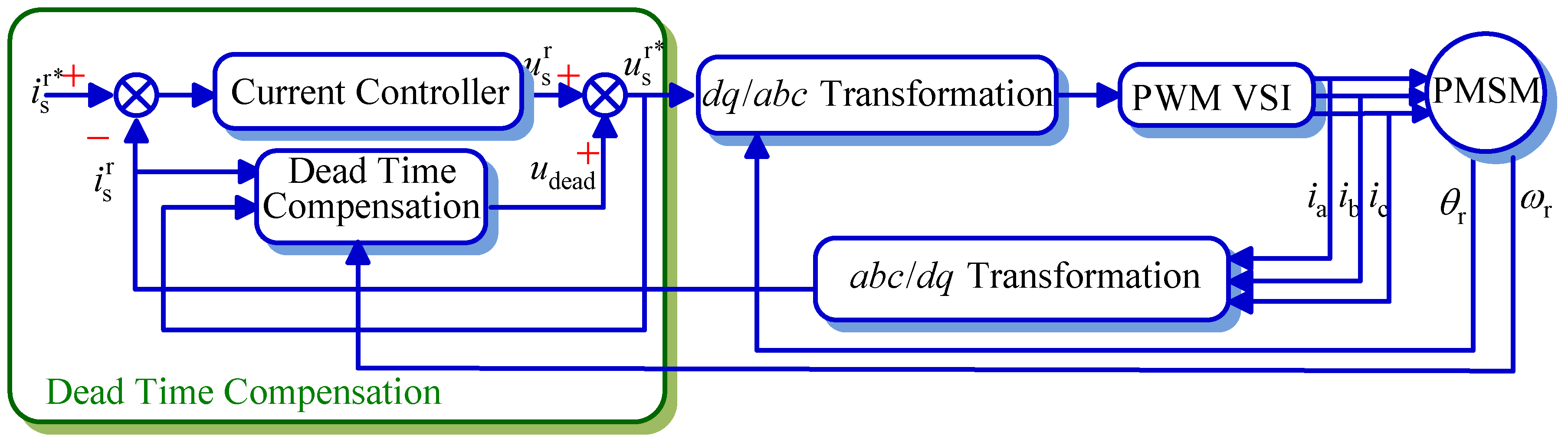
The basic idea of the disturbance observer is to construct a disturbance signal observer based on the error between the actual model and the reference model. The dead-time compensation method based on the disturbance observer uses a disturbance voltage observer based on making the output current as the input of the observer, and to estimate the disturbance voltage caused by dead time. The estimated disturbance voltage is used to compensate for dead time [73].
This method is implemented only with software; Figure 11 shows a schematic of the dead-time compensation method based on the disturbance observer [74]. In Figure 11, the reference input voltage usr* consists of the input reference and the disturbance voltage.
A novel procedure for PI feedback and lead-lag filter design is introduced in [75]. The proposed controller uses a robust tuning rule that is complemented be filters and is used for improving reference current and measurable disturbance responses. When perfect measurable disturbance compensation is not possible due to dead time, the proposed control provides a smaller integral error.
In order to improve the static and dynamic output performance of Uninterrupted Power Supply (UPS) inverters without adding sensors, a digital control strategy is proposed in [76]. This strategy uses the area equivalence principle to equate the dead-time voltage with a square-wave disturbance voltage, and regards the output current as the disturbance current of the control system, and the feed-forward control is used to compensate voltage and current. Because this method uses the differential operation of the output voltage to obtain the output filter capacitor current value, even if the current sensor is not used, the quasi-double loop control of the UPS inverter is still achieved.
In [77], an auto-tuning control system based on the modified Smith-predictor is proposed for use as an effective dead-time compensator. In order to improve the anti-interference ability, the system adds a feedback loop, used in a cascade structure. At the same time, this study provides several optimization rules of the main controller.
In the presence of interval parameter uncertainty, a novel method used to tune a PI compensator with dead time has been proposed [78]. Based on the optimization of load disturbance rejection, the method constrains the magnitude of the sensitivity and complementary sensitivity functions.
A simple and direct compensation technique to solve voltage distortion in a three-phase VSI has been introduced [79]. The proposed method calculates the practical voltage drop of the power devices in a sampling period according to the current polarity. The average voltage deviation is calculated by the difference between the actual voltage and reference voltage. The SVPWM switching intervals of each phase are derived by the average output voltages, and calculated according to the current polarity and nonlinear voltage distortion to compensate for the output voltage errors. The proposed compensation method is extremely easy to implement without any additional cost and software burden.
A new dead-time compensation method using the signal of the integrator output of the synchronous d-axis current regulator has been proposed [80]. The method can reduce voltage distortion by compensating for the output voltages of the d-q axis current regulator. This method does not require an additional hardware circuit, and can be adapted not only for the steady state but also for transient states.
This method relies on a simple principle and simple control structure, and needs few measurement parameters. Though it is easy to implement, the tracking step size of the method cannot balance response speed and accuracy. If the search step is too small, the search speed becomes slower; if the search step is too long, it is easy to cause oscillation and affect system stability.
3.8. Invalid Switch Elimination Method
The invalid switch elimination method, which is only valid for switches needing anti-parallel diodes such as IGBTs, has been the main method researched by scholars in recent years. The principle is that by analyzing the effective device of the converter, the invalid power device in the same bridge arm can be turned off, and the anti-parallel diode is freewheeling, so that there is no need for adding dead time. Therefore, the phenomenon of straight through of the upper and lower tubes of the same bridge arm can be avoided [81]. Because wrong current polarity detection can cause severe voltage distortion, even if the invalid switch elimination method does not consider turn on-off time and the voltage drop of power devices, it requires high-accuracy current polarity detection. The single-phase VSI circuit is an example for analyzing the mechanism of dead-time elimination.
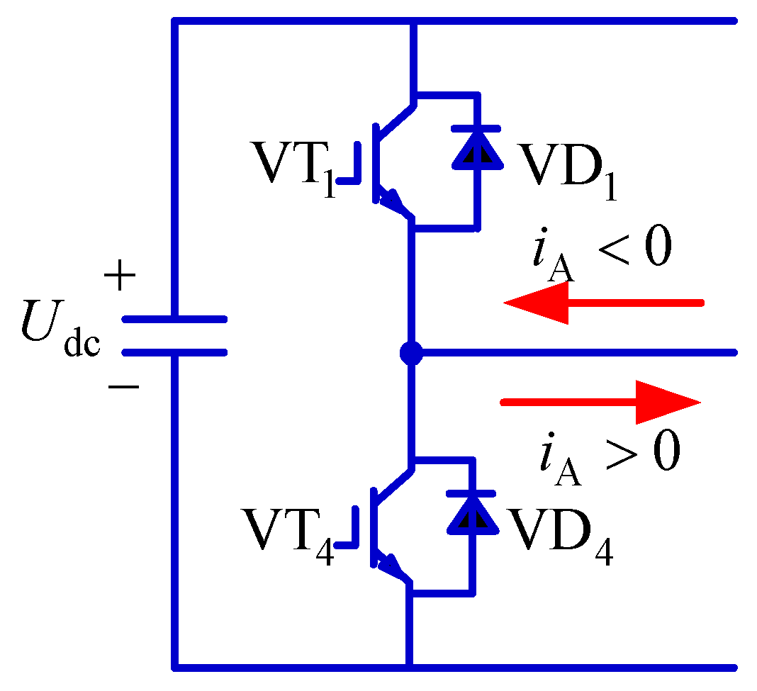
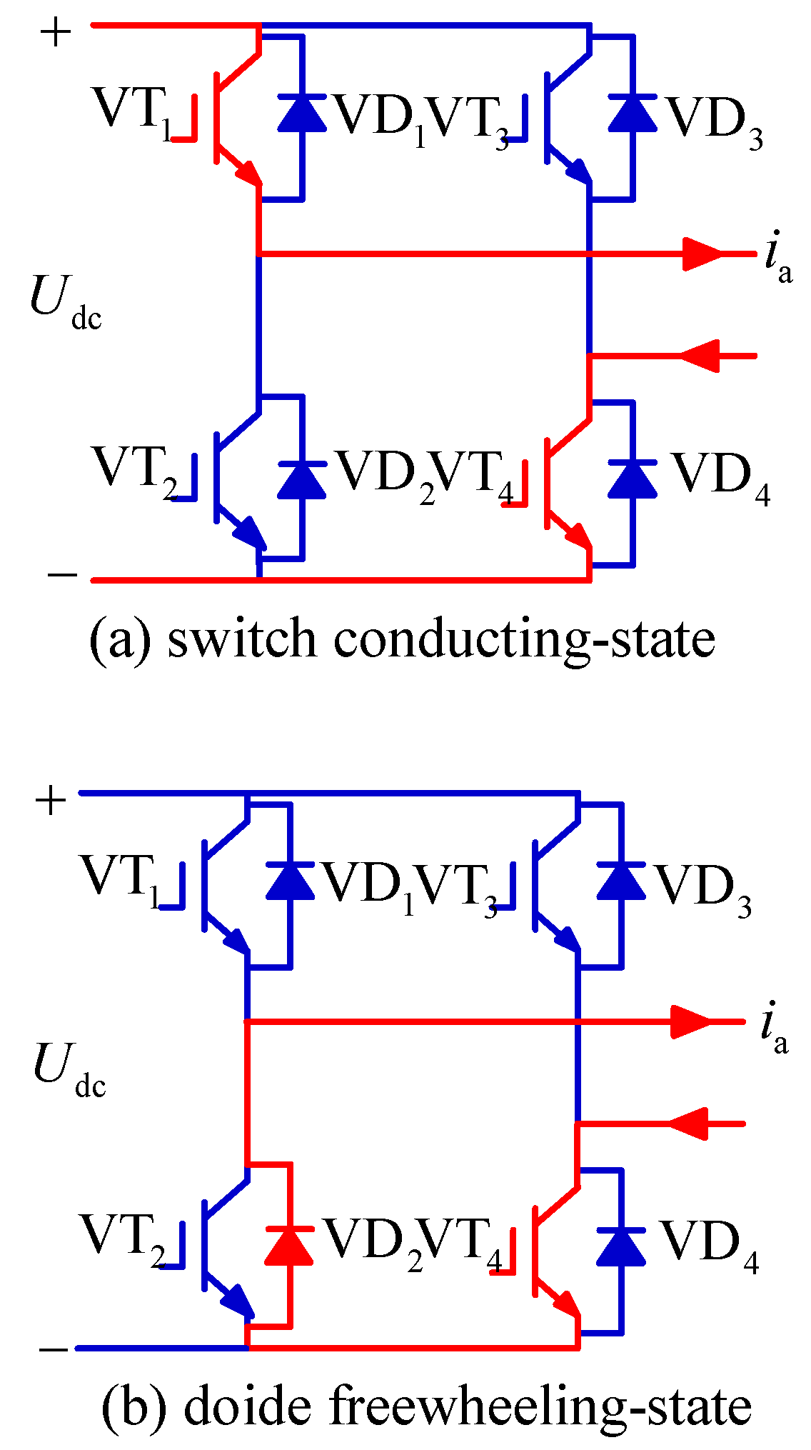
The following is an analysis of the principle of an invalid switch elimination method outside the threshold range. Instantaneously, the output current ia > 0, the driving signals of VT1, VT4 are turned on, and the inverter is in the power device conducting-state, as shown in Figure 12a. VT1 and VT4 are turned on, and VT2 and VT3 are turned off; when the driving signal of VT1 is turned off, the inverter is in the diode freewheeling state, as shown in Figure 12b. At this time, VT1 is turned off and VD2 is freewheeling. From the above analysis, no matter whether VT2 has a driving signal, ia does not flow through VT2, so VT2 can be called the invalid switch. Therefore, the driving signal of VT2 can be closed when ia > 0. Similarly, when the output current ia < 0, the driving signal of VT1 can be closed. This method not only ensures that the upper and lower power devices on the same bridge arm will not pass through, it does not affect the inverter output current ia waveform.
Because the polarity of the current changes frequently around the zero-crossing point, the invalid switch elimination method needs to add a threshold near the zero-crossing point [82]. Outside the threshold range, the invalid power device driving signals are turned off; within the threshold range, the inactive power device is reused, and the dead time is added to the driving signals of the upper and lower power devices in the same bridge arm. The key to this kind of method is how to select the threshold range. If the value is not accurate enough, the phenomenon of inaccurate compensation will occur near the threshold value, thus introducing harmonics.
Based upon the fact that the self-commutation switch device of an inverter phase would not turn on even though the gate-driving signal is supplied, the dead-time minimization algorithm is proposed in [83]. Using this method, the number of inverter switches is almost reduced to half that of the conventional method.
The invalid switch elimination method is adopted in dead-time compensation, used in the vector controlled PMSM system [84]. Above the threshold, the control strategy is based on the invalid switch elimination method; below the threshold, the dead-time compensation strategy is adopted to eliminate the voltage error caused by the current fluctuations and zero-current-clamping phenomena. This new strategy improves system stability and achieves desired control performance.
A novel IGBT gate-drive method is easily implemented in the IGBT gate driver of a PWM voltage source converter [85]. Using this method, the upper and lower IGBT gate drivers on the same bridge arm can receive the ideal complementary PWM signal without dead time. If the freewheeling diode conducts current, the gate driver turns off the IGBT, which parallels with this diode. This novel method can effectively operate with low current, low output frequency.
A dead-time elimination scheme for a converter that is controlled by PWM is proposed in [86]. The presented scheme proposes a current polarity detection circuit, which requires one power source only for a converter and a PWM control method without dead time. The proposed method dramatically improves output voltage loss and current distortion.
A novel strategy of dead-time elimination method for an H-bridge VSI and a new current polarity detection circuit used to remove dead time between signals are presented in [87]. The proposed detection circuit is based on the conduction states of two low anti-parallel diodes, and requires one power supply. Moreover, this proposed circuit can accurately detect low current polarity even at low output frequencies unlike current sensors.
A SVPWM control method based on a hybrid voltage vector has been put forward to avoid the effect of dead time [88]. This paper presents a novel method to compensate for dead-time effects by combining the 180° conduction type and 120° conduction type. In this method, an arbitrary space voltage vector is synthesized with the 12 basic voltage vectors. As a result, the novel control algorithm without dead time reduces the waveform distortion and harmonic content of the output voltage and improves the utilization of the DC bus voltage.
The invalid switch elimination method mainly relies on the accurate detection of the conduction state of each power device, so a hardware detection circuit is introduced in [89]. Due to the increase of hardware circuits, these methods have the disadvantages of increased experimental costs, poor reliability, and noise generation.
Based on the dead-time elimination method, a new switching strategy for PWM power converters has been proposed [90]. This strategy uses the polarity information of the reference current instead of the real current.
In [91], in order to deal with the dead-time control around the zero-current-crossing points, an immune algorithm based on the dead-time elimination PWM control strategy is proposed. This algorithm restricts the control sequence to a specified level around the zero-crossing region. Compared with traditional methods, the method can resolve the problem of detection around zero-the crossing point without a hardware detection circuit.
The dead-time effect in a synchronous d-q reference frame is studied in [92], and an average model of the inverter capable of capturing the low-frequency harmonic content in the load current along with the fundamental component is also developed. The average models are shown to consume less computation time.
In addition to the invalid switch method, other scholars proposed methods of not setting the dead time from the perspective of the control method [93]. A new dead-time elimination method for a nine-switch converter is proposed in [94]. The proposed method assumes that the unique switching elements of the nine-switch converter to operate at several subintervals are divided during a fundamental period. Due to the unidirectional conducting characteristics of the switching unit, the nine-switch converter can operate without dead time. In addition, for a special subperiod in which no switching unit can be used, a novel driving signal conversion method is proposed to eliminate dead time. A non-dead-time SPWM control strategy for a grid-connected inverter based on a modulation function is put forward in [95]. The phase separation control is used to achieve the decoupling of the three-phase grid-connected current and modulation function. Then the decoupled grid-connected current modulation function is used to perform the dead-time SPWM control. This control strategy is simple and effective, further guarantees the reliability of the dead-time modulation strategy, and removes the dependence of the traditional method on the hardware detection circuit.
The invalid switch elimination method enables the driving pulses of the upper and lower switching devices to alternate according to the current polarity. However, there is a certain degree of ambiguity in current zero-crossing and it is difficult to measure. Because the double second-order generalized integrator frequency-locked loop (DSOGI-FLL) has the noise-attenuation and frequency-adaptability characteristics, it is used to detect the current polarity. The DSOGI-FLL-based invalid switch elimination method is proposed in [96], and an improvement in the form of a delay compensation term is inserted in the DSOGI-FLL to compensate for both the current measurement delay and the control delay to minimize the current zero-crossing distortion. A dead-time elimination method of PWM controlled inverter is introduced in [97]. This method accurately determines the direction of the load current by detecting the operating conditions of the power devices and their antiparallel diodes. A low-cost circuit used to detect the operation of anti-parallel diodes is introduced in this study. Compared with complex compensators, this method has the characteristics of simple logic and flexible implementation.
It is known that the control is simple and convenient, easy to implement, and feasible. But this method cannot completely eliminate the influence of dead time, and it is necessary to set a certain dead time in a special interval.
3.9. The Volt-Second Equilibrium Theory Method
The volt-second equilibrium theory method divides the factors that cause output voltage distortion into the effects of dead time, switching time, and the voltage drop of the power device [98]. This method builds the converter circuit model off-line to achieve online compensation, and quantifies the effect of each factor on voltage distortion, since current polarity, detection and voltage error at the zero-crossing point of the current are the two key points of this method. Most of the dead-time compensation methods based on the volt-second equilibrium theory directly use the current sensor to detect the current polarity, but at the zero-crossing point, the current polarity detection is affected by the zero drift and noise.
Accurate current polarity judgment is achieved by detecting the situation of the two freewheeling diodes conducting in the same phase bridge [82]. However, the complicated hardware is required for this solution.
A feed forward voltage-second balancing strategy used in online conditions for monitoring data of SiC devices is employed in high frequency VSI applications [99]. The turn-off delay and rise/fall time of drain-source voltage signals are sent to the micro-controller, which is used in an algorithm to actively adjust the duty cycle of the driving signals to match the voltage-second of the non-ideal output voltage with an ideal output voltage-second. The monitoring system also allows the method to eliminate the need for accurate current detection.
A technique to compensate the effect of dead time in sinusoidal a PWM VSI is proposed in [100]. In order to avoid unfeasible pulse-widths of the driving signals, the compensation is implemented by adjusting the switching frequency. The variation of the switching frequency is defined by a simple scalar equation that can easily be included in the software of any drive system.
A feedback–feedforward phase voltage compensation method, based on derived expression of error voltage is proposed in [101]. Using a simple hardware circuit is used to obtain the actual output of the VSI as feedback with which precise compensation amplitude can be calculated. This method can also detect the current polarity by reconstructing the phase current from filtered current components with a Kalman filter. Using this method to compensate for dead time can improve the system stability.
For the duty cycle error of the drive signal, most studies use off-line compensation methods; however, these take a lot of time. In order to achieve online measurement of the error of the voltage duty cycle, a simple hardware circuit is designed in [102]. However, due to the parasitic capacitor of the power device, the slope of the terminal voltage will change at the zero-crossing point of the current. At the same time, this kind of hardware circuit will produce more duty cycle errors.
Based on the power device circuit, some models are formulated in [103]. These models mainly consider the parasitic capacitance, but rely on current detection, so the accuracy of the voltage error calculation at the zero-crossing point of current is still relatively low. Although the methods based on the principle of volt-second equilibrium seem to be accurate, this method needs to solve the problem of weak current measurement in a noisy environment.
A new method of deadtime effect compensation based on additional current measurements realized by analog-to-digital converters is proposed in [104]. Because the measurements are carried out at the time instants specified by a PWM strategy, they can easily estimate the voltage error caused by dead time. The voltage error is compensated for during the next switching period by modification of a reference voltage. Experimental results prove that the change of the time instant of additional measurements will give better results in the case of other low-pass filter parameters.
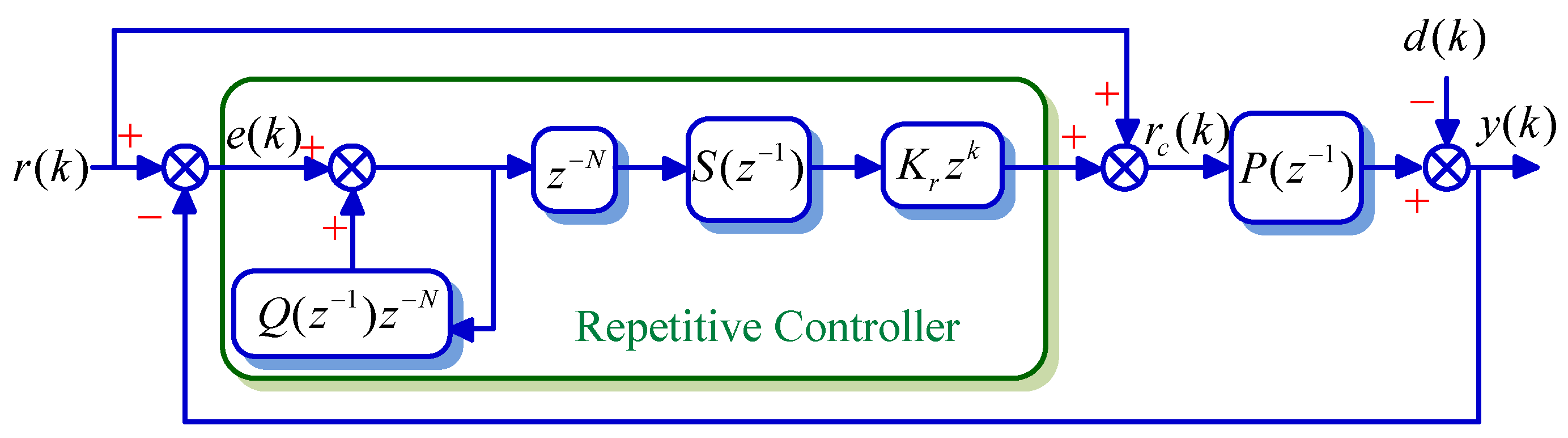
3.10. Repetitive Control
Dead time can be seen as a periodic disturbance signal that can be compensated by a repetitive controller [105]. Repetitive control is based on the internal model principle [106]. The internal model principle means that if the signal generator contains a reference command in a stable closed-loop system, the controlled output can follow the reference command without a steady-state error. If the system requires a zero steady-state error for the sinusoidal input, the model of the sine function should be included in the stable closed-loop transfer function. Due to the limited system bandwidth, it is impossible to eliminate all harmonics. The repetitive controller is mainly used to reduce the low-order harmonic distortion caused by dead time.
Figure 13 is a discrete block diagram of a repetitive controller used to compensate dead-time, where r(k) is the reference sinusoidal signal, y(k) is the output voltage of the inverter, d(k) is the disturbance signal caused by the dead-time, e(k) is the error voltage, and rc(k) is the reference instruction after being compensated. The transfer function P(z−1) represents the SPWM inverter model, Q(z−1) is a band limited filter, and S(z−1) is a compensator of the repetitive control loop. The repetitive controller calculates the compensation voltage according to the output voltage error, and the compensation voltage is added to the initial sinusoidal reference value for dead-time compensation.
Repetitive control can effectively suppress the harmonic current of the grid due to the infinite gain at each harmonic of the full frequency band. However, because repetitive control is equivalent to an infinite number of resonant terms connected in parallel, it also has problems, such as a narrow resonant frequency band and poor resistance to frequency fluctuation. Therefore, there is a control delay, which will affect the dynamic response of the system.
4. Discussion and Conclusion
The advantages and disadvantages of dead-time compensation methods and the inadequacies of various compensation methods are summarized in this article.
For the pulse-width adjustment method, due to the ambiguity of the zero-crossing point, the pulse width needs to be adjusted in each switching cycle in order to improve the accuracy of the current polarity determination. The existing method is either computationally complicated or increases the complexity of the system, so is still difficult to apply industrially.
Compared with the pulse-width adjustment method, the average voltage compensation technique is simple and convenient to control, and easy to implement. However, if the zero-crossing point detection accuracy is insufficient, the error compensation phenomenon will still occur. To solve this intractable problem, the voltage error is estimated online as a disturbance. The estimated value is fed back to the closed-loop control to avoid direction detection of the zero-crossing point or to reduce the accuracy requirement for direction detection.
In order to avoid the inaccuracy of current detection, the voltage feedback compensation technique directly detects the deviation voltage to eliminate the error caused by the dead-time effect. This method needs to add a complicated voltage detection circuit, and the detection circuit in actual industry will reduce the reliability and stability of system, so this method has almost no application.
The compensation effect of the current feedback compensation method is greatly affected by the accuracy of voltage or current detection. The accuracy of the current zero-crossing-point detection becomes the decisive factor determining the compensation effect. However, compared with the voltage feedback compensation technique, since the current needs to be detected in the control system, this method can estimate the feedback current without additional hardware, and the current detection is easier than the voltage detection. This method is simple in structure and easy to implement, and is widely used in practical industries, but requires increased detection accuracy.
The volt-second balance principle also relies on correct detection of the polarity of the current, and current polarity detection is greatly affected by zero drift and noise, which can easily cause false compensation. At the same time, this method requires a significant amount of software calculation, occupies lot of space resources, and is not easy to implement.
Due to the presence of high-frequency noise in the current detection channel, in the vicinity of the current zero-crossing point, error compensation will occur following error detection, which will aggravate the influence of the dead time. Therefore, all the above traditional compensation schemes have a common problem, namely, solving the current zero-crossing detection problem. In order to improve the traditional current detection methods, methods such as the invalid switch elimination method, the predictive current control method, and the adaptive method are proposed. However, these methods all require complicated software calculations, so are difficult to implement.
As with the voltage feedback compensation method, in order to avoid the direction detection of the current zero-crossing-point or to reduce the accuracy requirement for the direction detection, the invalid switch elimination method can eliminate dead time in most cases based on the optimization of the on/off state of a switching device, but cannot completely eliminate the dead-time effect. The method needs to set a certain dead time in a special interval by setting a threshold. For improvement of the invalid switch elimination method, one method is to set the threshold value, with the linear compensation within the threshold and the fixed value compensation beyond the threshold. Another method is to calculate the zero-crossing area width to improve zero-crossing detection.
Dead-time compensation methods based on disturbance observation means the disturbance voltage vector is no longer related to the polarity of the three-phase current, avoids detecting the polarity of the phase current, and can realize online real-time compensation for the dead-time effect. The method is simple to implement, better suppresses the zero-current-clamping phenomenon, and is widely used in industry, but requires a large amount of software calculation.
Similar to the disturbance observer, predictive current control does not need to detect the current direction, greatly simplifies the calculation process, and saves system resources. It is a low-cost and high-efficiency dead-time compensation method. Compared with traditional methods, it effectively improves the dynamic performance and steady state accuracy of the system. However, errors of system parameters can have a detrimental effect on dead-time compensation.
Similarly, the adaptive dead-time compensation method does not need to detect the current direction, which can effectively suppress the zero-current-clamping phenomenon. This improves the low-speed running performance of the system, which is simple and easy to implement. At the same time, this method can observe and compensate the dead-time effect in real time online, and avoid the undesired phenomenon of dead time caused by offline measurement. However, the fuzzy processing of information will lead to the reduction of control precision and dynamic quality of the system.
The repetitive control theory was developed for the characteristics of the dead zone effect and the periodicity of the output voltage distortion caused by phase-controlled rectification. It is applied to the control of the output voltage waveform of the inverter. Since this control operation is simple and has good reliability, the repetitive control technique has been widely used. However, repetitive control only suppresses periodic disturbances, and does not work for non-periodic disturbances.
Looking at the various dead-time effect compensation methods mentioned in the paper, we can clearly identify the research hotspots and trends of the dead-time compensation methods:
- (1)
- The traditional dead-time compensation schemes need to solve the zero-crossing-point current direction detection problem to avoid the zero-current-clamping phenomenon and the detection error of current direction. This problem can be solved in one of two ways: one is to develop a new method to avoid current detection, while the other is to improve the detection accuracy of current zero-crossing from the perspective of software and hardware.
- (2)
- Combining the intelligent control theory with the dead-time compensation algorithm optimizes the existing dead-time compensation methods and improves the compensation effect. The existing relevant literature attempts to combine intelligent control theory with dead-time compensation, but only in the laboratory stage, and is far from reaching the point of industrial application.
- (3)
- Develop higher-precision voltage and current detection instruments to improve detection accuracy. Hence, the existing compensation methods can be further applied.
Finally, the dead-time compensation is a key part for power converter, which directly affects the output performance, stability and reliability of the control system. Although in-depth research on dead-time compensation has been conducted and many solutions have been proposed, there are still certain problems or limitations for these algorithms in practical applications, especially for high and very high switching frequency operation of power converters with SiC and GaN devices [107]. The principles of various compensation methods have been comprehensively introduced and discussed in this article. This paper provides a useful reference regarding the selection and further research of dead-time compensation methods for power converters.
Author Contributions
This paper was a collaborative effort among all authors. investigation, Y.J., Y.Y., X.G.; review and editing J.Z., H.D., S.P.
Funding
This work is supported by the National Natural Science Foundation of China (51777181), Lite-On Research Funding, State Key Laboratory of Reliability and Intelligence of Electrical Equipment (No. EERIKF2018002), Hebei University of Technology, and Postdoctoral Research Program of Hebei Province (B2018003010).
Conflicts of Interest
The authors declare no conflict of interest.
References
- Huang, X.; Wang, K.; Li, G.; Zhang, H. Virtual inertia-based control strategy of two-stage photovoltaic inverters for frequency support in islanded micro-grid. Electronics 2018, 7, 340. [Google Scholar] [CrossRef]
- Smadi, I.A.; Albatran, S.; Alsyouf, M.A. Optimal control of a compact converter in an AC microgrid. Electronics 2018, 7, 102. [Google Scholar] [CrossRef]
- Popavath, L.N.; Kaliannan, P. Photovoltaic-STATCOM with low voltage ride through strategy and power quality enhancement in a grid integrated wind-PV system. Electronics 2018, 7, 51. [Google Scholar] [CrossRef]
- Senthilnathan, K.; Annapoorani, I. Multi-port current source inverter for smart microgrid applications: A cyber physical paradigm. Electronics 2019, 8, 1. [Google Scholar] [CrossRef]
- Alatawi, K.; Almasoudi, F.; Manandhar, M.; Matin, M. Comparative analysis of Si- and GaN-based single-phase transformer-less PV grid-tied inverter. Electronics 2018, 7, 34. [Google Scholar] [CrossRef]
- Ahmed, A.-S.; Jad, B.; Ahmed, F.A. Solid state transformers topologies, controllers, and applications: State-of-the-art literature review. Electronics 2018, 7, 298. [Google Scholar] [CrossRef]
- Singh, H.; Kumar, P.S.; Ali, M.U.; Lee, H.Y.; Khan, M.A.; Park, G.S.; Kim, H.-J. High frequency transformer’s parasitic capacitance minimization for photovoltaic (PV) high-frequency link-based medium voltage (MV) inverter. Electronics 2018, 7, 142. [Google Scholar] [CrossRef]
- Choi, J.W.; Sul, S.K. New dead time compensation eliminating zero current clamping in voltage-fed PWM inverter. In Proceedings of the 1994 IEEE Industry Applications Society Annual Meeting, Denver, CO, USA, 2–6 October 1994; Volume 2, pp. 977–984. [Google Scholar]
- Zhang, J.; Fang, L. An accurate approach of dead-time compensation for three-phase DC/AC inverter. In Proceedings of the 2009 4th IEEE Conference on Industrial Electronics and Applications, Xi’an, China, 25–27 May 2009; pp. 2929–2934. [Google Scholar]
- Yang, K.X.; Yang, M.; Lang, X.Y.; Lang, Z.; Xu, D. An adaptive dead-time compensation method based on Predictive Current Control. In Proceedings of the 2016 IEEE 8th International Power Electronics and Motion Control Conference (IPEMC-ECCE Asia), Hefei, China, 22–26 May 2016; pp. 121–125. [Google Scholar]
- Wang, S.J.; Luo, A. Study of dead-time effect and its compensation strategies. Trans. China Electrotech. Soc. 2009, 24, 111–119. [Google Scholar]
- Jeong, S.G.; Park, M.H. The analysis and compensation of dead-time effects in PWM inverters. IEEE Trans. Ind. Electron. 1991, 38, 108–114. [Google Scholar] [CrossRef]
- Cao, F.L.; Liu, J.J.; Zhang, Y. A switching strategy of dead-time elimination for pulse width modulation converters. In Proceedings of the 2015 IEEE 2nd International Future Energy Electronics Conference (IFEEC), Taipei, Taiwan, 1–4 November 2015; pp. 1–14. [Google Scholar]
- Zhou, H.W.; Wen, X.H.; Zhao, F.; Zhang, J.; Guo, X.H. A novel adaptive dead-time compensation strategy for VSI. Proc. CSEE 2011, 31, 26–32. [Google Scholar]
- Song, C.H.; Diao, N.Z.; Xue, Z.W.; Sun, X.R.; Guan, J. Tri-carrier sinusoidal pulse-width modulation without dead-time effects for converters. IET Power Electron. 2015, 8, 1941–1951. [Google Scholar] [CrossRef]
- Ikegami, S.; Hoshi, N.; Haruna, J. Experimental verification of dead-time compensation scheme for pulse width modulation scheme on six-switch two three-phase out put inverter. In Proceedings of the 2014 17th International Conference on Electrical Machines and Systems (ICEMS), Hangzhou, China, 22–25 October 2014; pp. 1420–1424. [Google Scholar]
- Bespal, K.; Savarovsky, V.J.; Stepin, V. Method for mesduring pulse width, which is less than the dead-time of measurement instrument. In Proceedings of the 2012 13th Biennial Baltic Electronics Conference, Tallinn, Estonia, 3–5 October 2012; pp. 311–314. [Google Scholar]
- Ogawa, M.; Ogasawara, S.; Takemoto, M. A feefback-type dead-time compensation method for high-frequency PWM inverter-Delay and pulse width characteristics. In Proceedings of the 2012 Twenty-Seventh Annual IEEE Applied Power Electronics Conference and Exposition (APEC), Orlando, FL, USA, 5–9 February 2012; pp. 100–105. [Google Scholar]
- Weerakoon, D.B.R.; Sandaruwan, B.L.L.; De Silva, R.T.T.; Abeyratne, S.G.; Rathnayake, D.B. A novel dead-time compensation scheme for PWM VSI drives. In Proceedings of the 2016 IEEE International Conference on Information and Automation for Sustainability (ICIAfS), Galle, Sri Lanka, 16–19 December 2016; pp. 1–6. [Google Scholar]
- Hwang, S.H.; Kim, J.M. Dead-time compensation method for voltage-fed PWM inverter. IEEE Trans. Energy Convers. 2010, 25, 1–10. [Google Scholar] [CrossRef]
- Kerkman, R.J.; Leggate, D.; Schlegel, D.W.; Winterhalter, C. Effects of parasitics on the control of voltage source inverter. IEEE Trans. Power Electron. 2003, 18, 140–150. [Google Scholar] [CrossRef]
- Patel, P.J.; Patel, V.; Tekwani, P.N. Pulse-based dead-time compensation method for selfbalanbcing space vector pulse width-modulated scheme used in a three-level inverter-fed induction motor drive. IET Power Electron. 2011, 4, 624–631. [Google Scholar] [CrossRef]
- Welchko, B.A.; Schulz, S.E.; Hiti, S.; Brian, A. Effects and compensation of dead-time and minimum pulse-width limitations in two-level PWM voltage source inverters. In Proceedings of the Conference Record of the 2006 IEEE Industry Applications Conference Forty-First IAS Annual Meeting, Tampa, FL, USA, 8–12 October 2006; pp. 889–896. [Google Scholar]
- Abhiram, T.; Reddy, P.S.; Prasad, P.V.N. Integrated dead-time SVPWM algorithm for indirect vector controlled two-level inverter fed induction motor drive. In Proceedings of the 2017 International Conference on Information, Communication, Instrumentation and Control (ICICIC), Indore, India, 17–19 August 2017; pp. 1–6. [Google Scholar]
- Yu, J.S.; Jin, G.; Cheng, S.L.; Ng, W.T. Digital dead-time control for an integrated tri-mode buck-boost DC-DC converter. In Proceedings of the 2015 9th International Conference on Power Electronics and ECCE Asia (ICPE-ECCE Asia), Seoul, Korea, 1–5 June 2015; pp. 1768–1771. [Google Scholar]
- Aizawa, N.; Kikuchi, M.; Kubota, H.; Miki, I.; Matsuse, K. Dead time effect and its compensation in common-mode voltage elimination of PWM inverter with auxiliary inverter. In Proceedings of the 2010 International Power Electronics Conference—ECCE ASIA, Sapporo, Japan, 21–24 June 2010; pp. 222–227. [Google Scholar]
- Liu, Y.; Huang, Q.; Dong, C. The direct pulse compensation of dead-time of APF. Procedia Eng. 2011, 15, 5355–5362. [Google Scholar] [CrossRef]
- Munoz, A.R.; Lipo, T.A. On-line dead-time compensation technique for open-loop PWM-VSI drive. IEEE Trans. Power Electron. 1999, 14, 683–689. [Google Scholar] [CrossRef]
- Zhao, B.; Song, Q.; Liu, W.; Sun, Y. Dead-time effect of the high-frequency isolated bidirectional full-bridge DC–DC converter: Comprehensive theoretical analysis and experimental verification. IEEE Trans. Power Electron. 2014, 29, 1667–1680. [Google Scholar] [CrossRef]
- Takashashi, H.; Obara, H.; Fujimoto, Y. Dead-time compensation for three-level flying capacitor inverter with phase shift PWM. AMC 2018, 41, 229–233. [Google Scholar]
- Gao, Y.; Wang, N.; Zhang, W.D. Disturbance observer based finite-time trajectory tracking control of unmanned surface vechicleswith unknown dead-zones. In Proceedings of the 32nd Youth Academic Annual Conference of Chinese Association of Automation (YAC), Hefei, China, 19–21 May 2017; pp. 263–268. [Google Scholar]
- Sawachan, H.; Liutanakul, P.; Wiwatcharagoses, N. A simple dead-time compensation technique for single-phase full-bridge PWM rectifier. In Proceedings of the 2017 International Electrical Engineering Congress (iEECON), Pattaya, Thailand, 8–10 March 2017; pp. 1–4. [Google Scholar]
- Alawieh, H.; Tehrani, K.A.; Azzouz, Y. A novel dead-time elimination strategy with zero crossing enhancement for voltage inverter. In Proceedings of the 7th IET International Conference on Power Electronics, Machines and Drives (PEMD 2014), Manchester, UK, 8–10 April 2014; pp. 1–5. [Google Scholar]
- Zhao, H.B.; Wu, Q.M.J.; Kawamura, A. An accurate approach of nonlinearity compensation for VSI inverter output voltage. IEEE Trans. Power Electron. 2004, 19, 1029–1035. [Google Scholar] [CrossRef]
- Putri, A.I.; Rizqiawan, A.; Rachmilda, T.; Haroen, Y.; Dahono, P.A. Suppressing dead-time effect in current-controlled three-phase PWM inverters by using virtual inductor. In Proceedings of the 2018 IEEE Applied Power Electronics Conference and Exposition (APEC), San Antonio, TX, USA, 4–8 March 2018; pp. 867–871. [Google Scholar]
- Leggate, D.; Kerkman, R.J. Pulse based dead-time compensator for PWM voltage inverters. IEEE Trans. Ind. Electron. 1997, 44, 191–197. [Google Scholar] [CrossRef]
- Choi, J.W.; Sul, S.K. A new compensation strategy reducing voltage/current distortion in PWM VSI systems operating with low output voltages. IEEE Trans. Ind. Appl. 1995, 31, 1001–1008. [Google Scholar] [CrossRef]
- Itkonen, T.; Luukko, J.; Sankala, A.; Laakkonen, T.; PÖllÄnen, R. Modeling and analysis of the dead-time effects in parallel PWM two-level three-phase voltage-source inverters. IEEE Trans. Power Electron. 2009, 24, 2446–2455. [Google Scholar] [CrossRef]
- Zhang, Z.; Xu, L. Dead-time compensation of inverters considering snubber and parasitic capacitance. IEEE Trans. Power Electron. 2014, 29, 3179–3187. [Google Scholar] [CrossRef]
- Ludek, B.; Lukas, O.; Miroslav, G. Effective dead-time compensation using adaptive harmonic compensator. IFAC-LiteraturesOnLine 2015, 48, 336–341. [Google Scholar] [CrossRef]
- Ludek, B. Online adaptive compensation scheme for dead-time and inverter nonlinearity in PMSM drive. IFAC-LiteraturesOnLine 2016, 49, 43–48. [Google Scholar]
- Kim, E.; Seong, U.; Lee, J.; Hwang, S. Compensation of dead time effects in grid-tied single-phase inverter using SOGI. In Proceedings of the 2017 IEEE Applied Power Electronics Conference and Exposition (APEC), Tampa, FL, USA, 26–30 March 2017; pp. 2633–2637. [Google Scholar]
- Urasaki, N.; Senjyu, T.; Kinjo, T.; Funabashi, T.; Sekine, H. Dead-time compensation strategy for permanent magnet synchronous motor drive taking zero-current clamp and capacitance effects into account. IEE Proc. Electr. Power Appl. 2005, 152, 845–853. [Google Scholar] [CrossRef]
- Blahnik, V.; Peroutka, Z.; Zak, J.; Talla, J. Elimination of dead-time effect causing current distortion of single-phase power converters. In Proceedings of the 2012 15th International Power Electronics and Motion Control Conference (EPE/PEMC), Novi Sad, Serbia, 4–6 September 2012; pp. 1–6. [Google Scholar]
- Liserre, M.; Blaabjerg, F.; Hansen, S. Design and control of an LCL-filter-based three-phase. IEEE Trans. Ind. Appl. 2005, 41, 1281–1291. [Google Scholar] [CrossRef]
- Hartmann, M.; Ertl, H.; Kolar, J.W. Current control of three-phase rectifier systems using three independent current controllers. IEEE Trans. Power Electron. 2013, 28, 3988–4000. [Google Scholar] [CrossRef]
- Yang, Y.H.; Zhou, K.L.; Blaabjerg, F. Analysis of dead-time harmonics in single-phase transformerless full-bridge PV inverters. In Proceedings of the 2018 IEEE Applied Power Electronics Conference and Exposition (APEC), San Antonio, TX, USA, 4–8 March 2018; pp. 1310–1315. [Google Scholar]
- Oliveira, A.C.; Jacobina, C.B.; Lima, A.M.N.; da Silva, E.R.C. Dead-time compensation in the zero-crossing current region. In Proceedings of the IEEE 34th Annual Conference on Power Electronics Specialist, Acapulco, Mexico, 15–19 June 2003; pp. 1937–1942. [Google Scholar]
- Futo, A.; Varjasi, I. Simple model based dead-time compensation using fast current measurement. AASRI Procedia 2014, 9, 146–151. [Google Scholar] [CrossRef]
- Park, D.M.; Kim, K.H. Parameter-independent online compensation scheme for dead-time and inverter nonlinearity in IPMSM drive through waveform analysis. IEEE Trans. Ind. Electron. 2014, 61, 701–707. [Google Scholar] [CrossRef]
- Cichowski, A.; Nieznanski, J. Self-tuning dead-time compensation method for voltage-source inverters. IEEE Power Electron. Lett. 2005, 3, 72–75. [Google Scholar] [CrossRef]
- Wu, M.G.; Zhao, R.X.; Tang, X.Z. Dead-time effects analysis and compensation of SPWM and SVPWM inverter. Proc. CSEE 2006, 26, 101–105. [Google Scholar]
- Urasaki, N.; Senjyu, T.; Uezato, K.; Funabashi, T. On-line dead-time compensation method for voltage source inverter fed motor drives. In Proceedings of the Nineteenth Annual IEEE Applied Power Electronics Conference and Exposition, Anaheim, CA, USA, 22–26 February 2004; pp. 122–127. [Google Scholar]
- Li, C.M.; Gu, Y.J.; Li, X.N.; Li, W.; He, X.; Dong, Z.; Chen, G.; Ma, C.; Zhang, L. Analysis and compensation of dead-time effect considering parasitic capacitance and ripple current. In Proceedings of the 2015 IEEE Applied Power Electronics Conference and Exposition (APEC), Charlotte, NC, USA, 15–19 March 2015; pp. 1501–1506. [Google Scholar]
- Sepe, R.B.; Lang, J.H. Inverter nonlinearities and discrete-time vector current control. IEEE Trans. Ind. Appl. 1994, 30, 62–70. [Google Scholar] [CrossRef]
- Peroutka, Z.; Blahník, V.; Zak, J.; Komrska, T. Compensation of low-frequency disturbances for traction converter with medium-frequency transformer for multi-system suburban units. In Proceedings of the 14th International Power Electronics and Motion Control Conference (EPE-PEMC 2010), Ohrid, Macedonia, 6–8 September 2010. [Google Scholar] [CrossRef]
- Muhlethaler, J.; Schweizer, M.; Blattmann, R.; Kolar, J.W.; Ecklebe, A. Optimal design of LCL harmonic filters for three-phase PFC rectifiers. IEEE Trans. Power Electron. 2013, 28, 3114–3125. [Google Scholar] [CrossRef]
- Oliva, A.; Chiacchiarini, H.; Aymonino, A.; Mandolesi, P. Reduction of total harmonic distortion in power inverter. Lat. Am. Appl. Res. 2005, 35, 89–93. [Google Scholar]
- Liu, L.; Deng, M.G. A new approach of dead-time compensation for voltage-fed PWM inverter. In Proceedings of the 2011 International Conference on Electric Information and Control Engineering, Wuhan, China, 15–17 April 2011; pp. 1039–1042. [Google Scholar]
- Guo, X.; Yang, Y.; Wang, X. Optimal space vector modulation of current source converter for dc-link current ripple reduction. IEEE Trans. Ind. Electron. 2019, 66, 1671–1680. [Google Scholar] [CrossRef]
- Shi, W.; Du, J.W. Sensorless control of Permanent Magnet Synchronous Motor based on rotating coordinate system considering dead-time. In Proceedings of the 2016 IEEE International Conference on Power and Renewable Energy (ICPRE), Shanghai, China, 21–23 October 2016; pp. 57–61. [Google Scholar]
- Dyer, J.; Zhang, Z.; Wang, F.; Costinett, D.; Tolbert, L.M.; Blalock, B.J. Dead-time optimization for SiC based voltage source converters using online condition monitoring. In Proceedings of the 2017 IEEE 5th Workshop on Wide Bandgap Power Devices and Applications (WiPDA), Albuquerque, NM, USA, 30 October–1 November 2017; pp. 15–19. [Google Scholar]
- Urasaki, N.; Senjyu, T.; Uezato, K.; Funabashi, T. Adaptive dead-time compensation strategy for permanent magnet synchronous motor drive. IEEE Trans. Energy Convers. 2007, 22, 271–280. [Google Scholar] [CrossRef]
- Yang, R.F.; Chen, W.; Yu, Y. Adaptive filter application in current vector dead-time compensation. Trans. China Electrotech. Soc. 2009, 24, 65–69. [Google Scholar]
- Zhou, J.W.; Li, H. Compensation method of dead-time effects based on kalman filter for PMSM inverter. Small Spec. Electr. Mach. 2009, 3, 25–27. [Google Scholar]
- Zhou, M.; Low, Q.W.; Siek, L. A high efficiency synchronous buck converter with adaptive dead-time control. In Proceedings of the 2016 International Symposium on Integrated Circuits (ISIC), Singapore, 12–14 December 2016; pp. 1–4. [Google Scholar]
- Qiu, T.; Wen, X.; Zhao, F. Adaptive-linear-neuron-based dead-time effects compensation scheme for PMSM drives. IEEE Trans. Power Electron. 2016, 31, 2530–2538. [Google Scholar] [CrossRef]
- Choi, C.H.; Cho, K.R.; Seok, J.K. Inverter nonlinearity compensation in the presence of current measurement errors and switching device parameter uncertainties. IEEE Trans. Power Electron. 2007, 22, 576–583. [Google Scholar] [CrossRef]
- Herran, M.A.; Fischer, J.R.; Gonzalez, S.A.; Judewicz, M.G.; Carrica, D.O. Adaptive dead-time compensation for grid-connected PWM inverters of single-stage PV systems. IEEE Trans. Power Electron. 2013, 28, 2816–2825. [Google Scholar] [CrossRef]
- Ngo, V.Q.B.; Rodriguez-Ayerb, P.; Olaru, S.; Niculescu, S.L. Model predictive direct power control of doubly fed induction generator with dead-time compensation. IFAC-LiteraturesOnLine 2017, 50, 8752–8757. [Google Scholar]
- Normey-Rico, J.E.; Lima, D.M.; Santos, T.L.M. Robustness of Nonlinear MPC for Dead-time Processes. IFAC-LiteraturesOnLine 2015, 48, 332–341. [Google Scholar] [CrossRef]
- Attaianese, C.; Tomasso, G. Predictive compensation of dead-time effects in VSI feeding induction motors. IEEE Trans. Ind. Appl. 2001, 37, 856–863. [Google Scholar] [CrossRef]
- Urasaki, N.; Senjyu, T.; Uezato, K.; Funabashi, T. An adaptive dead-time compensation strategy for voltage source inverter fed motor drives. IEEE Trans. Power Electron. 2005, 20, 1150–1160. [Google Scholar] [CrossRef]
- Kim, H.S.; Kim, K.H.; Youn, M.J. On-line dead-time compensation method based on time delay control. IEEE Trans. Contr. Syst. Technol. 2003, 11, 279–285. [Google Scholar]
- Rodríguez, C.; Julio, E.; Normey-Rico, J.E.; Guzmán, J.L.; Berenguel, M.; Dormido, S. Low-order feedback-feedforward controller for dead-time processes with measurable disturbances. IFAC-LiteraturesOnLine 2016, 49, 591–596. [Google Scholar] [CrossRef]
- Liu, Y.D.; Xing, Y.; Huang, L.P.; Sakane, M. Digitally controlled UPS inverter with dead-time and output current compensation. J. Tsinghua Univ. 2006, 46, 18–21. [Google Scholar]
- Kula, K.S. The autotuned dead-time compensating control system with improved disturbance rejection. IFAC-LiteraturesOnLine 2016, 49, 529–534. [Google Scholar] [CrossRef]
- Mercader, P.; Baños, A. A PI tuning rule for integrating plus dead-time processes with parametric uncertainty. ISA Trans. 2017, 67, 246–255. [Google Scholar] [CrossRef] [PubMed]
- Lee, D.H.; Ahn, J.W. A simple and direct dead-time effect compensation scheme in PWM-VSI. IEEE Trans. Ind. Appl. 2014, 50, 3017–3025. [Google Scholar] [CrossRef]
- Ryu, H.S.; Lim, I.H.; Lee, J.H.; Hwang, S.-H.; Kim, J.-m. A dead-time compensation method in voltage-fed PWM inverter. In Proceedings of the 2006 IEEE Industry Applications Conference Forty-First IAS Annual Meeting, Tampa, FL, USA, 8–12 October 2006; pp. 911–916. [Google Scholar]
- Zhang, B.; Huang, A.Q.; Chen, B.; Liu, Y. A new generation emitter turn-off (ETO) thyristor to reduce harmonics in the high power PWM voltage source converters. IEEE IPEMC 2004, 1, 327–331. [Google Scholar]
- Chen, L.H.; Peng, F.Z. Dead-time elimination for voltage source inverters. IEEE Trans. Power Electron. 2008, 23, 574–580. [Google Scholar] [CrossRef]
- Choi, J.S.; Yoo, J.Y.; Lim, S.W.; Kim, Y.S. A novel dead-time minimization algorithm of the PWM inverter. In Proceedings of the Conference Record of the 1999 IEEE Industry Applications Conference. Thirty-Forth IAS Annual Meeting (Cat. No.99CH36370), Phoenix, AZ, USA, 3–7 October 1999; pp. 2188–2193. [Google Scholar]
- Wang, H.; Wang, J.Z.; Wang, Z.J.; Zhao, J. A novel dead-time compensation in vector controlled PMSM system. In Proceedings of the 30th Chinese Control Conference, Yantai, China, 22–24 July 2011; pp. 3478–3483. [Google Scholar]
- Zhang, B.; Huang, A.Q.; Chen, B. A novel IGBT gate driver to eliminate the dead-time effect. In Proceedings of the Fortieth IAS Annual Meeting, Hong Kong, China, 2–6 October 2005; pp. 913–917. [Google Scholar]
- Lin, Y.K.; Lai, Y.S. Dead-time elimination of PWM-controlled inverter/converter without separate power sources for current polarity detection circuit. IEEE Trans. Ind. Electron. 2009, 56, 2121–2127. [Google Scholar]
- Alaweieh, H.; Riachy, L.; Tehrani, A.K.; Azzouz, Y.; Dakyo, B. A new dead-time effect elimination method for H-bridge inverters. In Proceedings of the IECON 2016—42nd Annual Conference of the IEEE Industrial Electronics Society, Florence, Italy, 23–26 October 2016; pp. 3153–3159. [Google Scholar]
- Long, L. A novel compensation method of dead time based on DSP. In Proceedings of the 27th Chinese Control and Decision Conference (2015 CCDC), Qingdao, China, 23–25 May 2015; pp. 3562–3565. [Google Scholar]
- Wang, Y.; Gao, Q.; Cai, X. Mixed PWM for dead-time elimination and compensation in a grid-tied inverter. IEEE Trans. Ind. Electron. 2011, 58, 4797–4803. [Google Scholar] [CrossRef]
- Cho, K.M.; Oh, W.S.; Kim, Y.T.; Kim, H.J. A new switching strategy for pulse width modulation (PWM) power converters. IEEE Trans. Ind. Electron. 2007, 54, 330–337. [Google Scholar] [CrossRef]
- Yuan, J.X.; Zhao, Z.; Chen, B.C. An immune-algorithm-based dead-time elimination PWM control strategy in a single-phase inverter. IEEE Trans. Power Electron. 2015, 30, 3964–3975. [Google Scholar] [CrossRef]
- Guha, A.; Narayanan, G. Average modeling of a voltage source inverter with dead-time in a synchronous reference freme. In Proceedings of the IEEE Innovative Smart Grid Technologies-Asia (ISGT Asia), Bangalore, India, 10–13 November 2013; pp. 1–6. [Google Scholar]
- Park, S.; Jahns, T.M. A novel dead-time elimination method using single-input enhanced phase-leg configuration. In Proceedings of the 38th IAS Annual Meeting on Conference Record of the Industry Applications Conference, Salt Lake City, UT, USA, 12–16 October 2003; pp. 2033–2040. [Google Scholar]
- Gao, F.; Tian, H.; Li, N. Dead-time elimination method of nine-switch converter. IET Power Electron. 2014, 7, 1759–1769. [Google Scholar] [CrossRef]
- Wang, Y.; Gao, N.; Luo, Y.H.; Cai, X. SPWM research for dead-time elimination in a three-phase three-level grid-connected inverter. Proc. CSEE 2006, 26, 13–17. [Google Scholar]
- Yan, Q.Z.; Zhao, R.D.; Yuan, X.B.; Ma, W.; He, J. A DSOGI-FLL-based dead-time elimination PWM for three-phase power converters. IEEE Trans. Power Electron. 2008, 2, 1. [Google Scholar] [CrossRef]
- Chen, L.; Peng, F.Z. Elimination of dead-time in PWM controlled inverters. In Proceedings of the IEEE APEC Annual Conference, Anaheim, CA, USA, 25 February–1 March 2007; pp. 306–309. [Google Scholar]
- Bolognani, S.; Peretti, L.; Zigliotto, M. Repetitive-control-based self-commissioning procedure for inverter nonidealities compensation. IEEE Trans. Ind. Appl. 2008, 44, 1587–1596. [Google Scholar] [CrossRef]
- Dyer, J.; Zhang, Z.Y.; Wang, F.; Costinett, D.; Tolbert, L.M.; Blalock, B.J. On-line condition monitoring based dead-time compensation for high frequency SiC voltage source inverter. In Proceedings of the 2018 IEEE Applied Power Electronics Conference and Exposition (APEC), San Antonio, TX, USA, 4–8 March 2018; pp. 1854–1860. [Google Scholar]
- Oliveira, A.C.; Jacobina, C.B.; Lim, A.M.N. Improved dead-Time compensation for Sinusoidal PWM inverters operating at high switching frequencies. IEEE Trans. Ind. Electron. 2007, 54, 2295–2304. [Google Scholar] [CrossRef]
- Wang, D.F.; Yang, B.W.; Zhu, C.; Zhou, C.; Qi, J. A Feedback-type phase voltage compensation strategy based on phase current reconstruction for ACIM drives. IEEE Trans. Power Electron. 2014, 29, 5031–5043. [Google Scholar]
- Zhou, D.S.; Rouaud, D.G. Dead-time effect and compensations of three-level neutral point clamp inverters for high-performance drive applications. IEEE Trans. Power Electron. 1999, 14, 782–788. [Google Scholar] [CrossRef]
- Mannen, T.; Fujita, H. Dead-time compensation method based on current ripple estimation. IEEE Trans. Power Electron. 2015, 30, 4016–4024. [Google Scholar] [CrossRef]
- Lewicki, A. Dead-time effect compensation based on additional phase current measurements. IEEE Trans. Ind. Electron. 2015, 62, 4078–4085. [Google Scholar] [CrossRef]
- Yang, Y.; Zhou, K.; Wang, H.; Blaabjerg, F. Analysis and mitigation of dead-time harmonics in the single-phase full-bridge PWM converter with repetitive controllers. IEEE Trans. Ind. Appl. 2018, 54, 5343–5354. [Google Scholar] [CrossRef]
- Costa-Castello, R.; Nebot, J.; Grino, R. Demonstration of the internal model principle by digital repetitive control of an educational laboratory plant. IEEE Trans. Educ. 2005, 48, 73–80. [Google Scholar] [CrossRef]
- Guo, X.; Zhang, X.; Guan, H.; Kerekes, T.; Blaabjerg, F. Three phase ZVR topology and modulation strategy for transformerless PV system. IEEE Trans. Power Electron. 2019, 34, 1017–1021. [Google Scholar] [CrossRef]
Figure 1.
Classification of dead-time compensation algorithms.

Figure 2.
Power switch device driving waveform and output voltage waveform.

Figure 3.
Phase a of voltage source inverter.

Figure 4.
Zero-current clamping diagram.

Figure 5.
Schematic diagram of pulse-width adjustment method.

Figure 6.
Schematic diagram of average voltage compensation method.

Figure 7.
Schematic diagram of current feedback compensation method.

Figure 8.
Schematic diagram of the voltage feedback compensation method.

Figure 9.
Adaptive estimation of dead-time compensation time based on disturbance observer.

Figure 10.
Adaptive estimation of dead-time compensation time based on disturbance observer.

Figure 11.
Schematic diagram of disturbance observer method.

Figure 12.
Current flow direction when the phase current ia > 0.

Figure 13.
Schematic diagram of repetitive control.

© 2019 by the authors. Licensee MDPI, Basel, Switzerland. This article is an open access article distributed under the terms and conditions of the Creative Commons Attribution (CC BY) license (http://creativecommons.org/licenses/by/4.0/).
Share and Cite
MDPI and ACS Style
Ji, Y.; Yang, Y.; Zhou, J.; Ding, H.; Guo, X.; Padmanaban, S. Control Strategies of Mitigating Dead-time Effect on Power Converters: An Overview. Electronics 2019, 8, 196. https://doi.org/10.3390/electronics8020196
AMA Style
Ji Y, Yang Y, Zhou J, Ding H, Guo X, Padmanaban S. Control Strategies of Mitigating Dead-time Effect on Power Converters: An Overview. Electronics. 2019; 8(2):196. https://doi.org/10.3390/electronics8020196
Chicago/Turabian StyleJi, Yi, Yong Yang, Jiale Zhou, Hao Ding, Xiaoqiang Guo, and Sanjeevikumar Padmanaban. 2019. "Control Strategies of Mitigating Dead-time Effect on Power Converters: An Overview" Electronics 8, no. 2: 196. https://doi.org/10.3390/electronics8020196
Note that from the first issue of 2016, this journal uses article numbers instead of page numbers. See further details here.