EE-TCAM: An Energy-Efficient SRAM-Based TCAM on FPGA


1
Department of Computer Engineering, Chosun University, 309 Pilmun-daero, Gwangju 61452, Korea
2
Department of Electrical Engineering, CECOS University of IT & Emerging Sciences, Peshawar 25000, Pakistan
*
Author to whom correspondence should be addressed.
Electronics 2018, 7(9), 186; https://doi.org/10.3390/electronics7090186
Submission received: 30 June 2018
/
Revised: 18 August 2018
/
Accepted: 7 September 2018
/
Published: 10 September 2018
Abstract
:Ternary content-addressable memories (TCAMs) are used to design high-speed search engines. TCAM is implemented on application-specific integrated circuit (native TCAMs) and field-programmable gate array (FPGA) (static random-access memory (SRAM)-based TCAMs) platforms but both have the drawback of high power consumption. This paper presents a pre-classifier-based architecture for an energy-efficient SRAM-based TCAM. The first classification stage divides the TCAM table into several sub-tables of balanced size. The second SRAM-based implementation stage maps each of the resultant TCAM sub-tables to a separate row of configured SRAM blocks in the architecture. The proposed architecture selectively activates at most one row of SRAM blocks for each incoming TCAM word. Compared with the existing SRAM-based TCAM designs on FPGAs, the proposed design consumes significantly reduced energy as it activates a part of SRAM memory used for lookup rather than the entire SRAM memory as in the previous schemes. We implemented the proposed approach sample designs of size 512 × 36 on Xilinx Virtex-6 FPGA. The experimental results showed that the proposed design achieved at least three times lower power consumption per performance than other SRAM-based TCAM architectures.
1. Introduction
Ternary content-addressable memory (TCAM) selects a word among stored ternary data based on its contents. It compares the search key with the entire stored TCAM words in parallel and outputs the address of the matching word in one cycle. The circuitry of a TCAM cell store and compare three states: 0, 1, and don’t-care state x. TCAM architecture is composed of an array of TCAM cells and a priority encoder (PE). Each TCAM cell comprises two SRAM cells storing a ternary bit and an associated comparison circuitry. Search lines (SLs) and match lines (MLs) perform the search operation. SLs provide search key bits to the corresponding cells of the TCAM words. The comparison results of each TCAM word are placed on the MLs. In case the matching of the search key is successful with more than one TCAM word, the PE selects the matching address with the highest priority. Figure 1 shows a sample design of TCAM. TCAM designed as a dedicated system in the application-specific integrated circuit (ASIC) is known as native TCAM.
TCAM finds its applications as look-up table in networking routers [1,2], as translations-look-aside buffers (TLBs) caches in microprocessors [3,4], as database accelerators in big-data analytics [4,5], as a filter when storing signature patterns in Internet-of-Things [6,7], as Local binary patterns recognition system in image processing and DNA sequence matching [8,9].
However, the dedicated bit comparison circuitry in each native TCAM cell lowers its memory density and the inherent massive parallelism makes native TCAM power hungry and expensive [10,11,12]. Moreover, the native TCAMs implemented in ASIC offer limited configurability which renders them less flexible to comply with the requirements and adaptation to the emerging trends in the applications of TCAMs [4,13,14].
The significant advancement in CMOS technology have made modern field-programmable gate arrays (FPGAs) an attractive choice for implementing emerging systems because of their offered massive parallelism with flexibility through on-the-fly reconfiguration. Contemporary SRAM-based FPGA device such as the 16-nm Xilinx Virtex UltraSCALE FPGA consist of a large amount of embedded memory called block RAMs (BRAMs) implemented in silicon substrate [15,16] that operates at high speed with low power consumption.
The demand for a high-speed flexible (re-configurable) and adaptable (easy for integration) TCAM configurations renders the embedded memories BRAMs on modern SRAM-based FPGAs attractive for the design of TCAMs. FPGAs implement TCAM using SRAM, by addressing SRAM with TCAM contents, and stores information for all data of TCAM table. Each SRAM word stores the existence and address information for a specific TCAM pattern. Existing SRAM-based TCAMs on FPGAs suffer from higher energy consumption as they consume excessive power to energize the entire SRAM memory used per lookup. For example, the SRAM-based TCAM design methodologies presented in recent works [13,17] consumed 2.5 and 3.2 to implement 89 b and 150 b TCAM tables using BRAMs on FPGA, respectively. The higher power consumption of SRAM-based TCAM designs becomes more severe for larger capacities.
The demand for a low power configurable and easy to integration TCAM design on FPGA makes the use of pre-classification approach practical for designing an energy-efficient SRAM-based TCAM (EE-TCAM). It works as follows: First, a TCAM table is partitioned into several sub-tables of balanced size in the classification stage. Second, in the SRAM-based implementation stage, each resultant TCAM sub-table is mapped to a separate row of cascaded SRAM blocks in the architecture. The proposed architecture selectively activates at most one row of SRAM blocks for each incoming TCAM word, thus attaining a substantial reduction in the overall dynamic power consumption.
The contributions of this work include:
- A TCAM table classification scheme is proposed to create several balanced-size groups of TCAM words. (Section 3.1)
- To the best of our knowledge, this is the first pre-classifier-based architecture for SRAM-based TCAM design, which achieves a considerable reduction in power consumption. (Section 3.2)
- The proposed design is implemented on a state-of-the-art FPGA. The proposed design is compared in detail with the existing FPGA realizations of TCAM with respect to power consumption per performance. Compared to prior work, our architecture exhibits at least 3× lower power consumption per performance. (Section 4)
- The trade-off details between the number of TCAM sub-tables M and the power consumption and throughput performance of the proposed design are presented. (Section 4.2)
The rest of this paper is organized as follows. Section 2 discusses the related work. The proposed TCAM table classification scheme and the proposed architecture are described in Section 3. Section 4 details the implementation results and performance evaluation of our proposed architecture. Section 5 concludes this paper. Table 1 lists the notations used in this paper.
2. Related Work
RAM-based associative content-addressable memory (CAM) was presented in a U.S. patent [18]. Its memory requirement increases exponentially with the increase in the pattern bits of CAM. For large bit patterns, it does not scale well in terms of the memory requirement, power consumption, and cost. Thus, it is not feasible to implement it on ASIC or FPGA platforms. Contrary to this our proposed work is memory-efficient and achieves a reduction in the dynamic power consumption by reducing the exponential increase in RAM memory to a linear increase. This is achieved by partitioning the large width TCAM bit patterns and then implementing them as a cascade of SRAM blocks in the proposed architecture.
A set-associative memory architecture implemented in hardware using the well-known hashing method was presented in [19]. It used RAM memory to implement CAM. However, in order to support TCAM functionality, the architecture suffered from inefficient memory utilization as it required two bits to encode ternary bits. On the contrary, our proposed solution does not encode ternary bits as two bits. The proposed solution addresses RAM memory with TCAM content, and each RAM word corresponds to a specific TCAM data pattern. In order to implement “don’t care” bits, more than one RAM word is selected. The proposed solution maps all possible TCAM data as RAM addresses.
Two types of FPGA implementations: a CAM based on Xilinx BRAM resource and a TCAM based on 16-bit shift registers (SRL16E)-are presented in Xilinx application note [20]. This emulation of TCAM on FPGA consumes one SRL16E for implementing two bits of TCAM. The shift register-based TCAM works efficiently for smaller TCAMs whereas, for implementing large storage capacity TCAMs, its design experience routing congestion and timing challenges. The proposed solution implements TCAM using the embedded SRAM memory blocks available on FPGAs and scales well in terms of speed and power consumption for implementing TCAMS of large storage capacity.
A low-power SRAM-based CAM design implementation on FPGA was presented in a previous work [17]. It performs a hierarchical lookup of the design-configured SRAM blocks. It achieves low power consumption by stopping subsequent SRAM lookup operations if a match is found in the present SRAM block. Although it reduces the average power consumption of the design, its worst-case power consumption remains high, which is not beneficial for the designed hardware as the hardware is designed based on the worst-case power consumption budget. In contrast, proposed work achieves a significant reduction in the worst-case power consumption of the implemented TCAM design.
Algorithmic solutions of TCAM implemented in SRAM-based pipelines on FPGAs suffer from non-deterministic throughput, long latencies, and inefficient memory usage [14,21]. A resource-efficient SRAM-based TCAM design was presented in [22], which stored the validation information of the TCAM words in distributed RAM blocks and the address information in the sub-blocks of the embedded SRAM memory blocks on FPGA. It completed the lookup operation for the incoming TCAM word via multiple high-speed sequential reads from the sub-blocks of its SRAM blocks and thus resulted in a degraded system throughput. The multiple high-frequency SRAM read operations per input word’s lookup resulted in higher dynamic power consumption of the design. Proposed work stores the validation and address information of the TCAM words in a single SRAM memory block and a single read operation is performed for completing the incoming TCAM word’s lookup. Thus, achieves higher throughput with reduced overall power consumption.
The design methodologies presented in [23,24,25] employs multiple distinct SRAM blocks for implementing TCAM functionality. These stores the TCAM word’s existence and address information separately in distinct sets of SRAM blocks. The Input TCAM word is applied to the first set of SRAM blocks to read its existence information and the address information is read from the second set of SRAM blocks. These TCAM design methodologies using multiple distinct SRAM blocks utilizes excessive SRAM memory. These works suffered from higher power consumption as the entire used excessive SRAM memory is activated for the incoming TCAM word lookup. In contrast, our proposed work stores the TCAM word’s existence and address information in a single RAM, thus realizing efficient memory usage. Moreover, proposed work achieves substantially reduced power consumption by activating at most one row of SRAM blocks for incoming TCAM words.
The SRAM-based design methodology with efficient storage efficiency in previous work [26] stored the existence and address information of TCAM word in a single SRAM memory block. A similar approach implemented an SRAM-based TCAM design using Xilinx BRAM or distributed RAM resource and provided an in-depth theoretical analysis in [13]. However, these works [13,26] energize all used SRAM memory blocks in the design for each incoming TCAM word’s lookup. Thus, consumes higher power consumption. In contrast proposed TCAM architecture selectively energizes a part of SRAM memory blocks used, achieving a substantial reduction in the overall dynamic power consumption of the design.
A recent work presented in [27] uses multipumping enabled multiported SRAM memory for implementing memory-efficient TCAM design on FPGA. It stores the sub-blocks of partitioned TCAM table in the shallow sub-blocks of BRAMs configured as multiported memories on FPGA.
For each incoming TCAM word, the existing SRAM-based TCAM architectures energize the entire SRAM memory of their architectures, resulting in excessive power consumption. In this work, we present a pre-classifier-based architecture for an energy-efficient SRAM-based TCAM design. We first classify a TCAM table into several TCAM sub-tables, which are further partitioned vertically. Each partitioned TCAM sub-table is implemented as a row of cascaded SRAM blocks in the proposed architecture. For each input TCAM word, at most one row of SRAM blocks is activated in the proposed design, significantly reducing the dynamic power consumption compared with the existing SRAM-based TCAMs.
3. Proposed Classification Scheme and Architecture
3.1. Proposed Classification Scheme for TCAM Table
The proposed design uses the bits extracted from specific bit positions of the TCAM words to classify the TCAM table words into groups called as TCAM sub-tables. In the proposed partitioning scheme we extract classification bits from the specified bit positions of the TCAM words to produce M sub-tables. For example, suppose two bits are used for the classification of a sample TCAM table of size is presented in Table 2. The TCAM table presented in Table 2 is classified using two different set of bit positions and as shown in Figure 2a,b, respectively. The sub-tables constructed based on the bit values (00, 01, 10, and 11) of bit positions are shown in Figure 2a. The number of TCAM words in the constructed sub-tables , , and varies based on the pattern of bits in the bit positions selected for the classification of Table 2. TCAM words with ‘x’ as bit value in the classification bit positions are stored in more than one sub-table. For example, the TCAM word at address 2 has the bit values of ‘x1’ at , and is thus stored in both sub-tables and . This redundancy expands the resultant TCAM sub-tables. The classification of any realistic dataset based on a specific set of bit positions may not necessarily produce sub-tables of the same size.
The proposed solution is based on the concept that the classification effectiveness of a set of bit positions varies from that of other bit positions for a specific dataset when the target of the classification is to construct balanced-size sub-tables. The classification example of the TCAM table in Table 2 using two different sets of bit positions is illustrated in Figure 2. It shows that the classification using is more effective for the TCAM table presented in Table 2, as the constructed sub-tables are of balanced size (2), when compared with the unbalanced size sub-tables constructed for bit positions (2, 3, 1, and 3) as explained above.
The constructed TCAM sub-tables are further mapped to the distinct rows of SRAM blocks in the proposed design. Figure 3 shows the mapping of the proposed classification scheme constructed sub-tables to SRAM memory. The contents of the four bit places of the unbalanced size sub-tables shown in Figure 2a and that of bit places of the balanced size sub-tables shown in Figure 2b are vertically partitioned into width of two, further mapped to the SRAMs with depth shown in Figure 3a,b, respectively. It clearly illustrates that the SRAM memory requirement for storing balanced size TCAM sub-tables constructed for bit positions is lower than that of unbalanced size sub-tables constructed for bit positions . The SRAM memory utilization overhead for pre-classifying the TCAM table contents in the proposed approach is minimal as balanced size sub-tables are constructed based on effective classification bits.
Algorithm 1 describes the proposed classification scheme. It classifies the TCAM words of the TCAM table into M sub-tables based on the comparison with the -bit values extracted from specific bit positions. The resultant sub-tables formed are tested for the maximum depth bound (MDB) of , where is the width of the configured SRAM blocks of the design on FPGA and is a scaling factor with integer values of . If the number of TCAM words in the resultant sub-tables exceeds MDB, a subsequent set of bit positions is used for the classification of the TCAM table. In the worst-case scenario, all subsets of bit positions from W bit positions are used to classify the TCAM table. The worst-case classification complexity of the proposed Algorithm 1 is reduced by using a relaxed MDB for the construction of sub-tables. An increase in the value of by one increases the MDB of the sub-tables by . A relaxed MDB of the sub-tables results in an increased RAM memory usage, as the resultant sub-tables are mapped to the SRAM blocks of the proposed design. The value of provides a trade-off between the time complexity of the proposed classification algorithm and the overall RAM memory usage of the proposed design.
The words of the M TCAM sub-tables are mapped to the M rows of the SRAM blocks of the architecture and the corresponding classification bit positions are used to configure the pre-classifier bit positions in the proposed architecture.
| Algorithm 1 Algorithm for the classification of the TCAM table into M sub-tables. |
|
3.2. Proposed Architecture
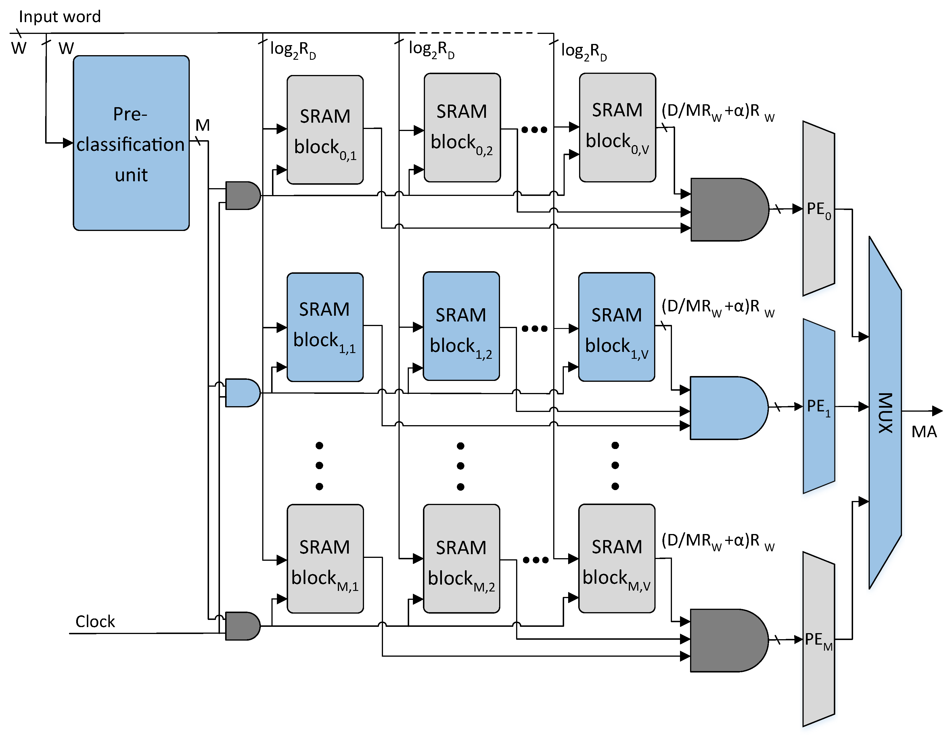
The TCAM table of size is classified into M sub-tables using the proposed classification scheme in Algorithm 1. The W-bit TCAM words of M sub-tables constructed are further divided into V sub-words of -bits. The resultant sub-partitions of the TCAM table are mapped to the M rows of the V SRAM blocks in the proposed architecture as shown in Figure 5. Each TCAM table sub-partition of size is implemented using an SRAM block. The SRAM block is a cascade of number of size SRAM blocks.
The proposed architecture comprises a pre-classifier unit and an SRAM-based TCAM. The pre-classifier unit of the proposed architecture is shown in Figure 4. The bit positions of the pre-classifier bits are specified using Algorithm 1 provided number of pre-classification bit positions. The pre-classifier bits are extracted from the bit positions of the incoming TCAM words using the number of select lines of W-to-1 multiplexers as shown in Figure 4. The extracted bits are further decoded to get an M-bit control signal that selectively activates at most one row of SRAM blocks of the proposed architecture.
The proposed SRAM-based TCAM architecture is shown in Figure 5. The incoming W-bit TCAM word is divided into V sub-words of -bits. The V sub-words are provided as addresses to the selected row of V SRAM blocks in parallel and V SRAM words are read. The V SRAM words read undergo a bit-wise AND operation and the resultant matching information bit vector is provided to the associated PE. The PE unit encodes the highest-priority matching bit position with the level high as the matching address.
3.3. Update Operation
The proposed TCAM design maps a new TCAM table dataset of the same size to the SRAM blocks of the configured architecture on FPGA. The SRAM blocks of the architecture has storage space for number of -bit TCAM sub-words. Algorithm 1 finds the set of classification bit positions, which makes TCAM sub-tables considering the maximum depth limitation of the configured architecture SRAM blocks on FPGA. The updated TCAM sub-tables are mapped to the SRAM blocks of the design on FPGA. The corresponding classification bit positions from Algorithm 1 configure the pre-classifier unit. The classification bits are now extracted from the updated set of bit positions for the incoming TCAM words. The proposed solution performs reconfiguration of the hardware design on FPGA in two cases: first, when the number of TCAM words in the Algorithm 1 constructed TCAM sub-tables exceeds the storage space of the configured architecture SRAM blocks, resulting in a relaxed MDB on the updated TCAM sub-tables. Second, when a TCAM table of different size is implemented in the proposed design.
During run-time, an update process of a TCAM word in proposed design includes the writing of the update word to the respective TCAM sub-table first, and the updated sub-table is then written to the corresponding row of SRAM blocks in the proposed architecture. The number of TCAM words in updated sub-tables is tested for the MDB of as this is the storage capacity of a row of configured SRAM blocks in proposed architecture. Owing to the presence of the don’t-care bits (x) in the TCAM words, EE-TCAM in the worst case writes the entire used SRAM memory to complete the update process of a TCAM word. The partitioned sub-tables are written in parallel to the corresponding SRAM blocks in the proposed architecture, and the depth of the configured BRAMs determines the update latency of EE-TCAM design. The update latency of EE-TCAM is 513 cycles. While native TCAMs have also comparable worst case TCAM write time of O(N) for updating a TCAM word, where N is the number of words in the TCAM table [28,29,30,31].
4. FPGA Implementation Results & Performance Evaluation
We used a Xilinx Virtex-6 XC6VLX760-2FF1760 FPGA device for the proposed EE-TCAM design of a TCAM. Three design cases of TCAM were implemented with the following design parameters: denoted EE-TCAM-I and denoted EE-TCAM-II using 36 b BRAMs and denoted EE-TCAM-III using 18 b BRAMs. Algorithm 1 was used to classify 512 TCAM words into , 8, and 16 TCAM sub-tables.
The minimum depth limitation on the configuration of BRAM is . The storage capacity of BRAMs is maximum when used in minimum depth configurations of for 18 b size and for 36 b size [13,27]. Thus, the contents of the TCAM sub-tables formed were further divided into sub-words of width , which addresses the configured BRAMs of depth . The resultant sub-partitions were mapped to the configured BRAMs of the EE-TCAM designs on FPGA. The proposed EE-TCAM designs were implemented using Xilinx ISE 14.7 and were verified via behavioural and post-route simulations using the Xilinx ISim simulator. The Xilinx Place and Route report was used to evaluate the FPGA resource utilization and speed. The Xilinx Xpower Analyzer tool [32] was used for the estimation of the dynamic power consumption of the design. Table 3 lists the FPGA resource utilization parameters such as slice registers, LUTs, and BRAMs of the EE-TCAM I, II, and III designs for implementing a TCAM table.
4.1. Scalability of EE-TCAM
We have evaluated the scalability of EE-TCAM using important performance evaluation metrics, like memory utilization, clock rate, and power consumption implementing various sizes of TCAM tables. Table 4 lists the memory utilization, clock rate, and power consumption for the TCAM tables of width , 54, and 72 for depth , 512, and 1024 with TCAM sub-tables of , 8, and 16 configurations implemented using EE-TCAM.
Table 4 shows that the memory usage of EE-TCAM grows proportionally with an increase in the width or depth of the implemented TCAM table size. The memory usage of EE-TCAM remains same with an increase in the number of TCAM sub-tables M.
Table 4 shows that EE-TCAM achieves high clock rates of (233 MHz–346 MHz) for the specified sizes of TCAM tables. EE-TCAM achieve a linear decrease in the clock rate with a linear increase in the depth or width of the implemented TCAM tables when M is constant. The delay in EE-TCAM increases because of the increase in the number of wide bit-wise ANDing operations and associated routing delay. The EE-TCAM showed an increase in the clock rate with an increase in the number of TCAM sub-tables M owing to the reduced bit-wise ANDing complexity of a row of SRAM blocks.
Table 4 illustrates that the dynamic power consumption of EE-TCAM increases linearly with an increase in the width and depth of the implemented TCAM table when M is constant. The memory usage of a row of SRAM memory blocks increases with an increase in the size of the implemented TCAM table, which results in an increase in the power consumption of EE-TCAM. The dynamic power consumption of EE-TCAM decreases with an increase in the number of TCAM sub-tables M owing to the activation of reduced size SRAM memory of a row of SRAM blocks.
The EE-TCAM design implementations for depth and width , 54, 72 with does not follow the same performance trend in memory usage and power consumption as shown in Table 4. The memory usage of EE-TCAM implementations for the specified sizes with gets double from that of the same sizes implementations with . This is because the memory size of a row of SRAM blocks for remains the same (72 b) as that of and the number of rows of SRAM-blocks gets double (16 from 8). This is due to the minimum 36 bit width configuration for depth = 512 of 18 b BRAM on Xilinx FPGAs [15]. This increase in the memory usage of a row of SRAM-blocks results in the increased power consumption of proposed EE-TCAM implementations for specified sizes with as illustrated in the Table 4.
4.2. Trade-Off between the Number of TCAM Sub-Tables (M) and Performance
The number of TCAM sub-tables M determines the depth of the sub-tables formed, and when mapped to the SRAM memory determines the RAM memory usage of each row of SRAM blocks in the EE-TCAM design. An increase in M reduces the RAM memory usage of each row of SRAM blocks in the EE-TCAM design. This leads to a reduction in the overall power consumption of the proposed design with an increase in M as the reduced memory of at most one row of SRAM blocks is energized per lookup for incoming words.
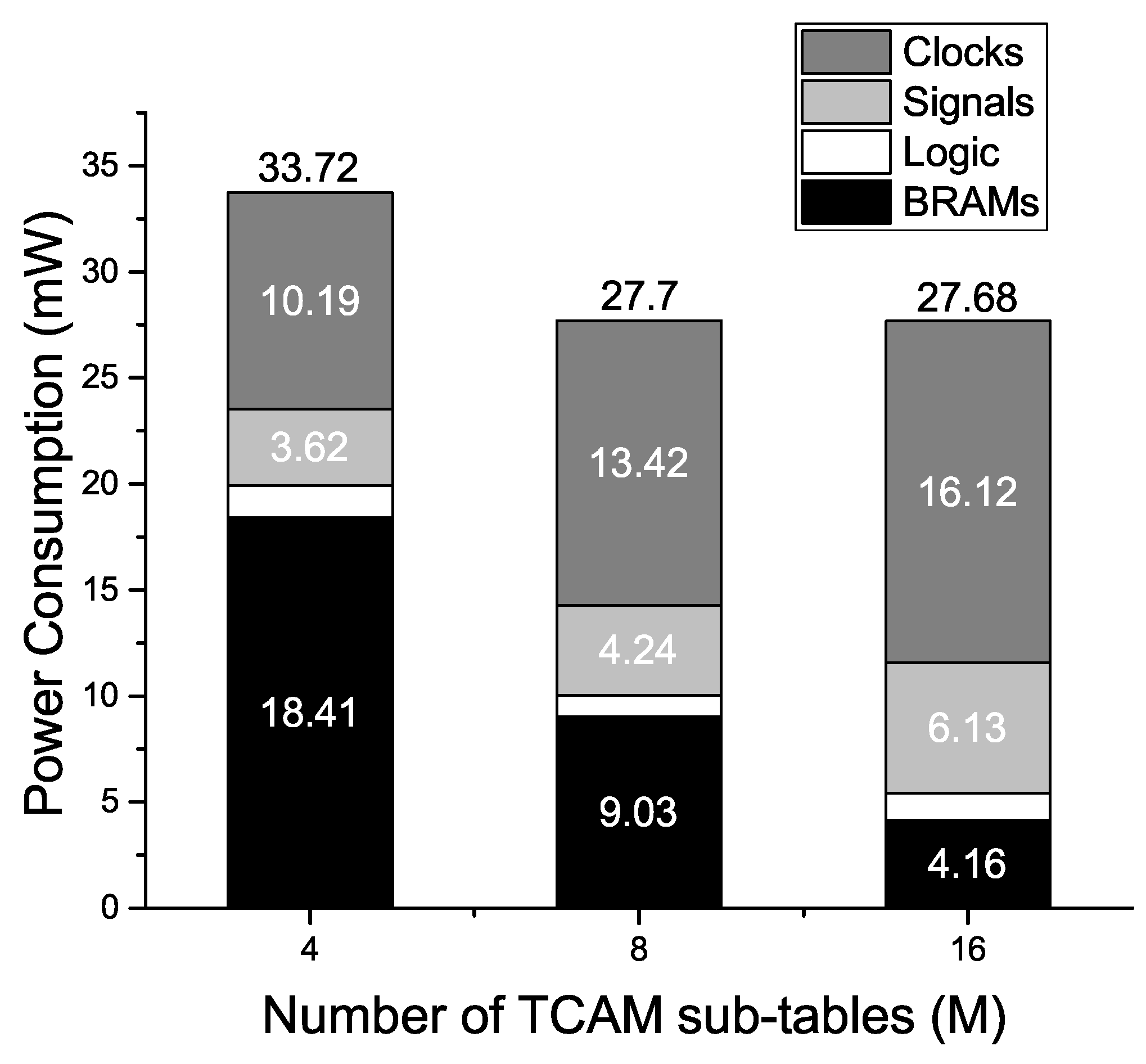
To evaluate the impact of the change in M on the performance of the proposed EE-TCAM design, we implemented three EE-TCAM design cases I, II, and III, with , 8, and 16, respectively, using Xilinx BRAM resource for a TCAM table. The RAM memory usage of a row of SRAM blocks in the EE-TCAM design shows a decreasing trend with the increase in the value of M. The proposed design cases EE-TCAM I, II, and III, activate at most one row of SRAM blocks per lookup i.e., 288 b (8 BRAMs of size 36 b), 144 b (4 BRAMs of size 36 b), and 72 b (4 BRAMs of size 18 b), respectively. The individual BRAM resource power consumption of the EE-TCAM design cases I, II, and III shows a decreasing trend 18.41 , 9.03 , and 4.16 , respectively, as shown in Figure 6. The increase in the number of TCAM sub-tables M has a decreasing impact on the size of the activated BRAM resource in the proposed EE-TCAM design. Thus, the individual power consumption of the BRAM resource in proposed EE-TCAM shows a decreasing trend with an increasing value of M.
The overall power consumption of the EE-TCAM design III does not show an exactly decreasing trend. This is because of the increased individual clock and signal resource power consumption as shown in Figure 6. Compared to EE-TCAM I with , the number of design units in EE-TCAM II () and EE-TCAM III () doubles and quadruples, respectively. Thus, EE-TCAM II and EE-TCAM III show an increased clock distribution and interconnect power consumption as shown in Figure 6.
The operational frequencies of the EE-TCAM design listed in Table 4 shows an increasing trend with the increase in the number of TCAM sub-tables M, owing to the reduced complexity of bit-wise AND operation and PE units, as the size of the SRAM words decreases with the increase in the value of M.
Overall, the trade-off between the number of TCAM sub-tables M and the power consumption and throughput performance of the proposed EE-TCAM design showed that considerable improvement in performance is achieved with an increase in M.
4.3. Power Consumption
RAM memory accounts for a major proportion of the power consumption in the design of SRAM-based TCAMs. In the SRAM-based solutions of TCAM, the depth of TCAM table determines the width of the SRAM memory and is implemented as a cascade of number of SRAM blocks. The width of TCAM table is encoded as the address of the SRAM memory and implemented as a cascade of number of SRAM blocks. The minimum achieved power consumption of the existing SRAM-based TCAM design methodologies on FPGAs in terms of the SRAM blocks used can be formulated using Equation (1) as follows:
where denotes the power consumption of an SRAM block. The proposed design activates at most number of entire used SRAM blocks to complete the lookup operation for an incoming TCAM word. Thus, achieves a considerable reduction in the power consumption by a factor of M as expressed using Equation (2).
4.4. Power Consumption per Performance
Table 5 presents a comparison of the proposed EE-TCAM designs with the existing state-of-the-art FPGA-based TCAMs with respect to the power consumption per performance from [33] given by Equation (3).
For a fair comparison with [22] and [13], we normalized their reported frequency and power consumption results to 40-nm CMOS technology using Equation (4), modified from previous study in [34].
The normalized frequency and power consumption factors are denoted as and , respectively, when considering 40-nm CMOS technology and a supply voltage of 1.0 V. The original results of the respective works are reported in parentheses.
EE-TCAM designs I, II, and III implemented a (18 b) TCAM table consuming 33.72 , 27.70 , and 27.68 , respectively, and achieved the speed of 276 MHz, 321 MHz, and 336 MHz, respectively. Thus, the power consumption per performance of EE-TCAM I, II, and III was 6.8 (W/(TCAMDepth.Gb/s)), 4.8 (W/(TCAMDepth.Gb/s)), and 4.6 (W/(TCAMDepth.Gb/s)), respectively. Table 5 shows that the power consumption per performance of the proposed EE-TCAM designs is at least three times lower than that of UE-TCAM [26], which is the lowest among the existing FPGA implementations of SRAM-based TCAMs.
5. Conclusions
TCAM-based search engines play an important role in networking routers. Researchers have proposed several SRAM-based TCAM designs on re-configurable hardware. Native TCAMs and existing SRAM-based TCAMs suffer from higher power consumption.
This paper presented a pre-classifier-based architecture for an energy-efficient SRAM-based TCAM, which selectively activates at most one row of SRAM blocks for lookup rather than activating the entire SRAM memory as in the existing architectures. The experimental results showed that the proposed design exhibits at least three times lower power consumption per performance than the existing FPGA realizations of TCAM.
Author Contributions
I.U. devised the main research idea, performed the experiments on tools and wrote the paper. Authors Z.U. and J.-A.L. provided guidance, suggestions, and reviewed the writing of this work. Z.U. and J.-A.L. supervised and finalized this paper.
Funding
This study was supported by research fund from Chosun University, 2018.
Conflicts of Interest
The authors declare no conflict of interest.
References
- Etzel, K. Answering IPv6 Lookup Challenges; Technical Article; Cypress Semiconductor Corporation: San Jose, CA, USA, 2004. [Google Scholar]
- Taylor, D.E. Survey and taxonomy of packet classification techniques. ACM Comput. Surv. (CSUR) 2005, 37, 238–275. [Google Scholar] [CrossRef]
- Haigh, J.R.; Clark, L.T. High performance set associative translation lookaside buffers for low power microprocessors. Integr. VLSI J. 2008, 41, 509–523. [Google Scholar] [CrossRef]
- Karam, R.; Puri, R.; Ghosh, S.; Bhunia, S. Emerging trends in design and applications of memory-based computing and content-addressable memories. Proc. IEEE 2015, 103, 1311–1330. [Google Scholar] [CrossRef]
- Nguyen, X.T.; Hoang, T.T.; Nguyen, H.T.; Inoue, K.; Pham, C.K. An FPGA-Based Hardware Accelerator for Energy-Efficient Bitmap Index Creation. IEEE Access 2018, 6, 16046–16059. [Google Scholar] [CrossRef]
- Chang, M.F.; Lin, C.C.; Lee, A.; Chiang, Y.N.; Kuo, C.C.; Yang, G.H.; Tsai, H.J.; Chen, T.F.; Sheu, S.S. A 3T1R nonvolatile TCAM using MLC ReRAM for frequent-off instant-on filters in IoT and big-data processing. IEEE J. Solid-State Circuits 2017, 52, 1664–1679. [Google Scholar] [CrossRef]
- Tsai, H.J.; Yang, K.H.; Peng, Y.C.; Lin, C.C.; Tsao, Y.H.; Chang, M.F.; Chen, T.F. Energy-efficient TCAM search engine design using priority-decision in memory technology. IEEE Trans. Very Large Scale Integr. Syst. 2017, 25, 962–973. [Google Scholar] [CrossRef]
- Mujahid, O.; Ullah, Z.; Mahmood, H.; Hafeez, A. Fast Pattern Recognition Through an LBP Driven CAM on FPGA. IEEE Access 2018, 6, 39525–39531. [Google Scholar] [CrossRef]
- Lin, K.J.; Wu, C.W. A low-power CAM design for LZ data compression. IEEE Trans. Comput. 2000, 49, 1139–1145. [Google Scholar]
- Agrawal, B.; Sherwood, T. Modeling TCAM power for next generation network devices. In Proceedings of the 2006 IEEE International Symposium on Performance Analysis of Systems and Software, Austin, TX, USA, 19–21 March 2006; pp. 120–129. [Google Scholar] [Green Version]
- Lambiri, C.; Senior staff architect IDT. Private communication, 2008.
- Akhbarizadeh, M.J.; Nourani, M.; Vijayasarathi, D.S.; Balsara, T. A nonredundant ternary CAM circuit for network search engines. IEEE Trans. Very Large Scale Integr. Syst. 2006, 14, 268–278. [Google Scholar] [CrossRef] [Green Version]
- Jiang, W. Scalable ternary content addressable memory implementation using FPGAs. In Proceedings of the Ninth ACM/IEEE Symposium on Architectures for Networking and Communications Systems (ANCS), San Jose, CA, USA, 21–22 October 2013; pp. 71–82. [Google Scholar]
- Jiang, W.; Prasanna, V.K. Parallel IP lookup using multiple SRAM-based pipelines. In Proceedings of the IEEE International Symposium on Parallel and Distributed Processing (IPDPS 2008), Miami, FL, USA, 14–18 April 2008; pp. 1–14. [Google Scholar]
- Xilinx. Virtex-6 FPGA Memory Resources User Guide. Available online: http://www.xilinx.com (accessed on 15 July 2018).
- Alfke, P. Creative Uses of Block RAM; White Paper: Virtex and Spartan FPGA Families; Xilinx: San Jose, CA, USA, 2008. [Google Scholar]
- Qian, Z.; Margala, M. Low power RAM-based hierarchical CAM on FPGA. In Proceedings of the 2014 International Conference on ReConFigurable Computing and FPGAs (ReConFig), Cancun, Mexico, 8–10 December 2014; pp. 1–4. [Google Scholar]
- Somasundaram, M. Circuits to Generate a Sequential Index for an Input Number in a Pre-Defined List of Numbers. U.S. Patent 7,155,563, 26 December 2006. [Google Scholar]
- Cho, S.; Martin, J.; Xu, R.; Hammoud, M.; Melhem, R. CA-RAM: A High-Performance Memory Substrate for Search-Intensive Applications. In Proceedings of the IEEE International Symposium on Performance Analysis of Systems Software, (ISPASS 2007), San Jose, CA, USA, 25–27 April 2007; pp. 230–241. [Google Scholar] [CrossRef]
- Locke, K. Parameterizable content-addressable memory. In Xilinx Application Note XAPP1151; Xilinx: San Jose, CA, USA, 2011. [Google Scholar]
- Jiang, W.; Prasanna, V.K. Large-scale wire-speed packet classification on FPGAs. In Proceedings of the ACM/SIGDA International Symposium on Field Programmable Gate Arrays, Monterey, CA, USA, 22–24 February 2009; pp. 219–228. [Google Scholar]
- Ahmed, A.; Park, K.; Baeg, S. Resource-Efficient SRAM-Based Ternary Content Addressable Memory. IEEE Trans. Very Large Scale Integr. Syst. 2017, 25, 1583–1587. [Google Scholar] [CrossRef]
- Ullah, Z.; Ilgon, K.; Baeg, S. Hybrid partitioned SRAM-based ternary content addressable memory. IEEE Trans. Circuits Syst. I Regul. Pap. 2012, 59, 2969–2979. [Google Scholar] [CrossRef]
- Ullah, Z.; Jaiswal, M.K.; Cheung, R.C. Z-TCAM: An SRAM-based architecture for TCAM. IEEE Trans. Very Large Scale Integr. Syst. 2015, 23, 402–406. [Google Scholar] [CrossRef]
- Ullah, Z.; Jaiswal, M.; Cheung, R. E-TCAM: An Efficient SRAM-Based Architecture for TCAM. Circuits Syst. Signal Process. 2014, 33, 3123–3144. [Google Scholar] [CrossRef]
- Ullah, Z.; Jaiswal, M.K.; Cheung, R.C.C.; So, H.K.H. UE-TCAM: An ultra efficient SRAM-based TCAM. In Proceedings of the 2015 IEEE Region 10 Conference (TENCON 2015), Macau, China, 1–4 November 2015; pp. 1–6. [Google Scholar] [CrossRef]
- Ullah, I.; Ullah, Z.; Lee, J.A. Efficient TCAM Design Based on Multipumping-Enabled Multiported SRAM on FPGA. IEEE Access 2018, 6, 19940–19947. [Google Scholar] [CrossRef]
- Wang, Z.; Che, H.; Kumar, M.; Das, S.K. CoPTUA: Consistent policy table update algorithm for TCAM without locking. IEEE Trans. Comput. 2004, 53, 1602–1614. [Google Scholar] [CrossRef]
- Shah, D.; Gupta, P. Fast incremental updates on Ternary-CAMs for routing lookups and packet classification. In Proceedings of the Hot Interconnects, Stanford, CA, USA, 16–18 August 2000. [Google Scholar]
- Shah, D.; Gupta, P. Fast updating algorithms for TCAM. IEEE Micro 2001, 21, 36–47. [Google Scholar] [CrossRef]
- Syed, F.; Ullah, Z.; Jaiswal, M.K. Fast Content Updating Algorithm for an SRAM based TCAM on FPGA. IEEE Embed. Syst. Lett. 2017, 10, 73–76. [Google Scholar] [CrossRef]
- Xilinx. Xilinx Xpower Analyzer. Available online: http://www.xilinx.com (accessed on 15 July 2018).
- Nakahara, H.; Sasao, T.; Iwamoto, H.; Matsuura, M. LUT Cascades Based on Edge-Valued Multi-Valued Decision Diagrams: Application to Packet Classification. IEEE J. Emerg. Sel. Top. Circuits Syst. 2016, 6, 73–86. [Google Scholar] [CrossRef]
- Chen, O.C.; Sheen, R.B. A power-efficient wide-range phase-locked loop. IEEE J. Solid-State Circuits 2002, 37, 51–62. [Google Scholar] [CrossRef]
Figure 1.
A TCAM: (MLSAs: Match line sense amplifiers).
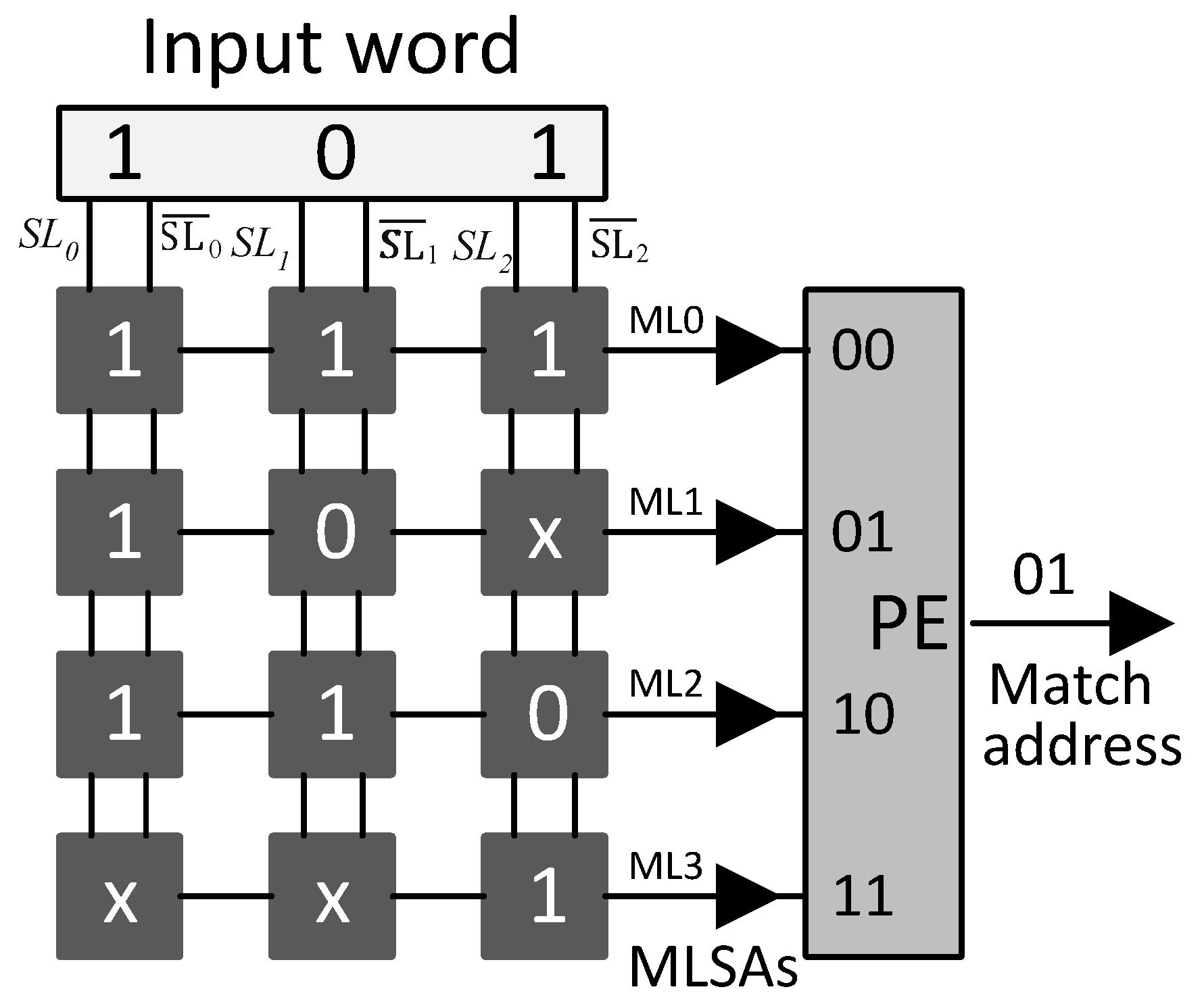
Figure 2.
Example of the proposed classification algorithm: (a) Description of Classification based on set of bit positions . (b) Description of Classification based on set of bit positions .
Figure 2.
Example of the proposed classification algorithm: (a) Description of Classification based on set of bit positions . (b) Description of Classification based on set of bit positions .
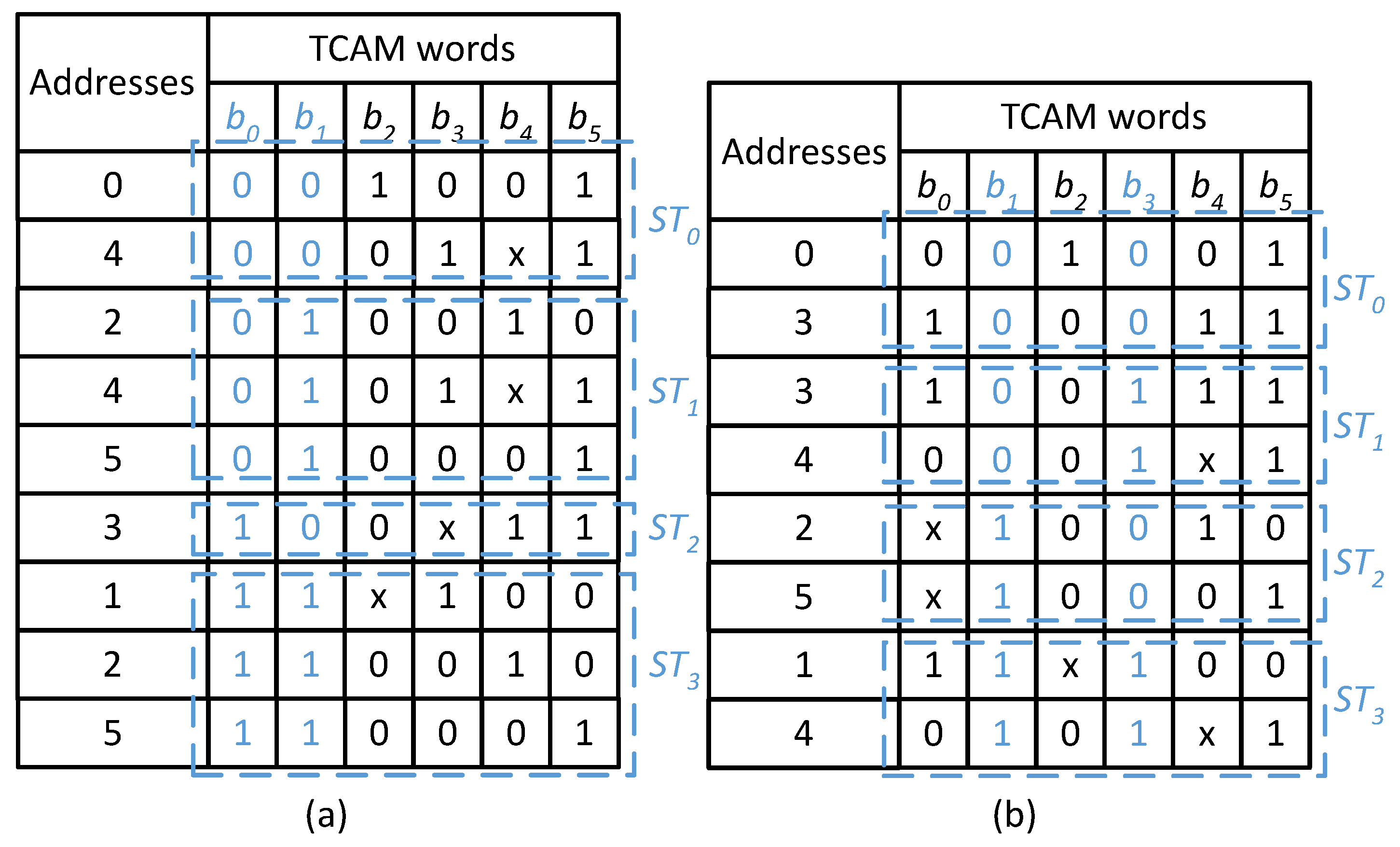
Figure 3.
Example of mapping proposed classiifcation scheme constructed TCAM-subtables to SRAM: (a) Mapping TCAM sub-tables contents to SRAM constructed based on set of bit positions . (b) Mapping TCAM sub-tables contents to SRAM constructed based on set of bit positions .
Figure 3.
Example of mapping proposed classiifcation scheme constructed TCAM-subtables to SRAM: (a) Mapping TCAM sub-tables contents to SRAM constructed based on set of bit positions . (b) Mapping TCAM sub-tables contents to SRAM constructed based on set of bit positions .

Figure 4.
Architecture of the pre-classifier unit: (S: Select lines for extracting the pre-classification bits, : Number of bits in the, : Number of pre-classifier bits, M: Number of enable control bits for the M rows of SRAM blocks).
Figure 4.
Architecture of the pre-classifier unit: (S: Select lines for extracting the pre-classification bits, : Number of bits in the, : Number of pre-classifier bits, M: Number of enable control bits for the M rows of SRAM blocks).
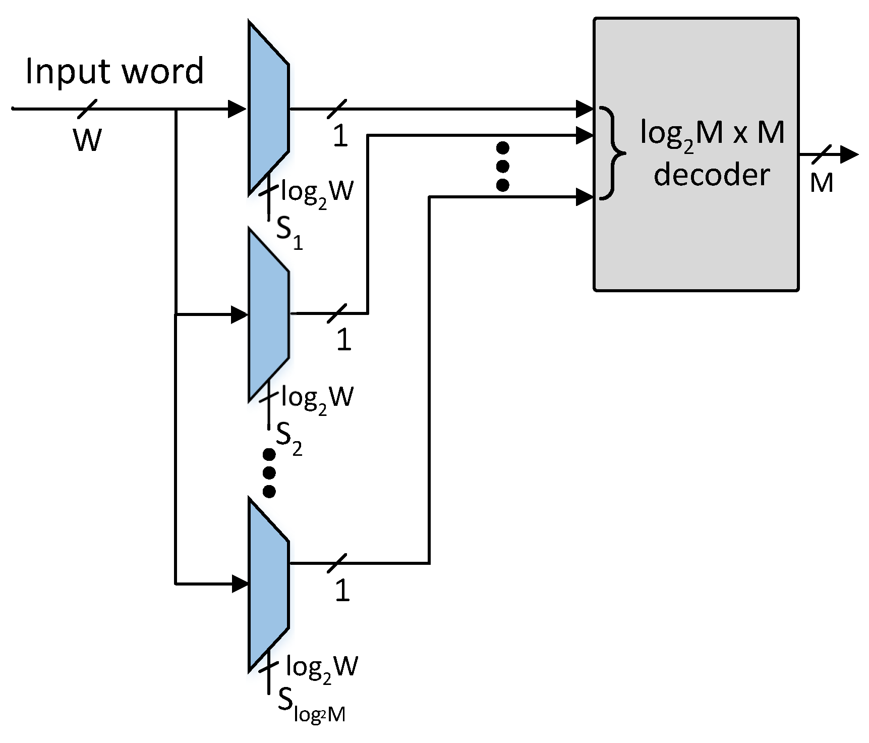
Figure 5.
Proposed overall architecture: (M: Number of rows of SRAM blocks, V: Number of SRAM blocks in a row, PE: priority encoder unit, MA: matching address, : Address bits of the configured SRAM blocks, : Configured SRAM blocks words width).
Figure 5.
Proposed overall architecture: (M: Number of rows of SRAM blocks, V: Number of SRAM blocks in a row, PE: priority encoder unit, MA: matching address, : Address bits of the configured SRAM blocks, : Configured SRAM blocks words width).

Figure 6.
Trade-Off between the Number of TCAM Sub-Tables (M) and Power Consumption Performance.

Table 1.
List of notations used.
| Notation | Description |
|---|---|
| D | Depth of TCAM table |
| W | Width of TCAM table |
| Depth of the configured SRAM blocks | |
| Width of the configured SRAM blocks | |
| Address bits of the configured SRAM blocks | |
| M | Number of TCAM sub-tables/Rows of the SRAM blocks in architecture |
| V | Number of SRAM blocks in each row of the proposed architecture |
Table 2.
A TCAM table of size 6 × 6.
| Address | TCAM Words |
|---|---|
| 0 | 001001 |
| 1 | 11x100 |
| 2 | x10010 |
| 3 | 100x11 |
| 4 | 0x01x1 |
| 5 | x10001 |
Table 3.
FPGA resource utilization of EE-TCAM on Xilinx Virtex-6.
| Proposed Design Cases | Slice Registers | LUTs | BRAMs |
|---|---|---|---|
| EE-TCAM-I [M = 4] | 652 | 1535 | 32 |
| EE-TCAM-II [M = 8] | 687 | 1455 | 32 |
| EE-TCAM-III [M = 16] | 712 | 1419 | 32 |
Table 4.
Performance trend for increasing EE-TCAM depth (D), width (W) in various configurations.
| No. of TCAM | TCAM Depth | 256 | 512 | 1024 | ||||||
|---|---|---|---|---|---|---|---|---|---|---|
| Sub-Tables | TCAM Width | 36 | 54 | 72 | 36 | 54 | 72 | 36 | 54 | 72 |
| Memory utilization (b) | ||||||||||
| 576 | 864 | 1152 | 1152 | 1728 | 2304 | 2304 | 3456 | 4608 | ||
| 576 | 864 | 1152 | 1152 | 1728 | 2304 | 2304 | 3456 | 4608 | ||
| 1152 | 1728 | 2304 | 1152 | 1728 | 2304 | 2304 | 3456 | 4608 | ||
| Clock rate (MHz) | ||||||||||
| 326 | 313 | 299 | 276 | 260 | 243 | 264 | 252 | 233 | ||
| 338 | 323 | 308 | 321 | 306 | 261 | 297 | 272 | 246 | ||
| 346 | 335 | 317 | 336 | 316 | 270 | 310 | 293 | 251 | ||
| Power consumption () | ||||||||||
| 26.3 | 37.3 | 55.2 | 33.7 | 52.9 | 70 | 62 | 89.1 | 134 | ||
| 23.6 | 36.8 | 51.3 | 27.7 | 50.3 | 64.5 | 36.1 | 59.1 | 80 | ||
| 32.1 | 54.2 | 72.7 | 27.7 | 47.9 | 61.4 | 30.9 | 55.5 | 72.1 | ||
Table 5.
Comparison of the power consumption per performance with previous works.
| Architecture | FPGA | TCAM Size | Speed | AM/L (a) | Throughput | Power | PC/P (b) |
|---|---|---|---|---|---|---|---|
| (D × W) | (MHz) | (Gb/s) | (mW) | ||||
| Locke [20] | Virtex-6 | 512 × 36 | 166 | 2304 | 5.8 | 253 | 85 |
| Qian [17] | Virtex-6 | 504 × 180 | 133 | 5040 | 23.4 | 2548 | 216 |
| REST [22] | Kintex-7 | 72 × 28 | 35 (50) | 36 | 1.4 | 161 (113) | 2329 |
| HP-TCAM [23] | Virtex-6 | 512 × 36 | 118 | 2016 | 4.2 | 188 | 89 |
| Z-TCAM [24] | Virtex-6 | 512 × 36 | 159 | 1440 | 5.6 | 109 | 38 |
| E-TCAM [25] | Virtex-6 | 512 × 36 | 164 | 1440 | 5.8 | 91 | 31 |
| UE-TCAM [26] | Virtex-6 | 512 × 36 | 202 | 1152 | 7.1 | 78 | 21 |
| Jiang [13] | Virtex-7 | 1024 × 150 | 97 (139) | 9792 | 20.4 | 4587 (3211) | 315 |
| EE-TCAM-I | Virtex-6 | 512 × 36 | 276 | 288 | 9.7 | 33.72 | 6.8 |
| EE-TCAM-II | Virtex-6 | 512 × 36 | 321 | 144 | 11.3 | 27.7 | 4.8 |
| EE-TCAM-III | Virtex-6 | 512 × 36 | 336 | 72 | 11.8 | 27.68 | 4.6 |
(a)AM/L: Activated memory/lookup (kb); (b)PC/P: Power consumption/performance (W/(TCAMDepth.Gb/s).
© 2018 by the authors. Licensee MDPI, Basel, Switzerland. This article is an open access article distributed under the terms and conditions of the Creative Commons Attribution (CC BY) license (http://creativecommons.org/licenses/by/4.0/).
Share and Cite
MDPI and ACS Style
Ullah, I.; Ullah, Z.; Lee, J.-A. EE-TCAM: An Energy-Efficient SRAM-Based TCAM on FPGA. Electronics 2018, 7, 186. https://doi.org/10.3390/electronics7090186
AMA Style
Ullah I, Ullah Z, Lee J-A. EE-TCAM: An Energy-Efficient SRAM-Based TCAM on FPGA. Electronics. 2018; 7(9):186. https://doi.org/10.3390/electronics7090186
Chicago/Turabian StyleUllah, Inayat, Zahid Ullah, and Jeong-A Lee. 2018. "EE-TCAM: An Energy-Efficient SRAM-Based TCAM on FPGA" Electronics 7, no. 9: 186. https://doi.org/10.3390/electronics7090186
Note that from the first issue of 2016, this journal uses article numbers instead of page numbers. See further details here.