Improved Step Load Response of a Dual-Active-Bridge DC–DC Converter


Faculty of Information Technology, Macau University of Science and Technology, Macau, China
*
Author to whom correspondence should be addressed.
Electronics 2018, 7(9), 185; https://doi.org/10.3390/electronics7090185
Submission received: 10 August 2018
/
Revised: 3 September 2018
/
Accepted: 6 September 2018
/
Published: 9 September 2018
(This article belongs to the Special Issue Applications of Power Electronics)
Abstract
:This paper proposes a fast load transient control for a bidirectional dual-active-bridge (DAB) DC/DC converter. It is capable of maintaining voltage–time balance during a step load change process so that no overshoot current and DC offset current exist. The transient control has been applied for all possible transition cases and the calculation of intermediate switching angles referring to the fixed reference points is independent from the converter parameters and the instantaneous current. The results have been validated by extended experimental tests.
1. Introduction
In recent decades, with the increasing concern in environment issue and energy crisis, the power conversion systems (PCSs) have been using widely in renewable generation facilities. The dual-active-bridge (DAB) converter seems to be a preferred choice of PCSs in various bidirectional DC/DC applications, such as energy storage systems, electric vehicles (EV) and solid state transformers, because of its high power density, low cost and zero-voltage-switching (ZVS) features [1,2,3,4,5,6,7,8,9,10,11,12,13,14].
Interfacing two different DC sources, the DAB converter is a kind of bidirectional DC–DC converter, which consists of two full bridges linked by a high-frequency (HF) transformer with the turn ratio of , whose circuit layout is shown in Figure 1. Including the leakage inductance of the transformer, the inductor is connected on the primary side as the main energy transfer device. The resistor , which normally is small enough to be neglected in steady-state analysis, is an equivalent resistance of and the total winding resistance of HF transformer. The eight active switches can be controlled by their gating signals with 50% duty cycle and fixed switching frequency. The voltage gain of DAB converter is defined as , where is the input voltage and is the output voltage. and are two HF voltages generated on the primary side and the secondary side, respectively. The power is manipulated by controlling the phase-shift angles among each switch arms.
Depending on the number of varying phase-shifts, there are several control schemes for a DAB converter, which are single-phase-shift (SPS) control, extended-phase-shift control (EPS), dual-phase-shift (DPS) control and triple-phase-shift (TPS) control. The SPS control is the simplest control strategy that is easy to implement. However, it has many disadvantages such as high circulating power and loss of ZVS if the converter gain is away from unity [1,2]. In addition, the TPS control has three independent phase-shifts to be controlled, which makes it costly and more complex in real implementation [3,4]. In contrast, EPS control and DPS control are compromised ones with both enough flexibility and easy implementation [5,6,7,8,9,10,11,12,13,14]. To make a step load change in a DAB converter, one or more phase-shift angles should be adjusted accordingly. The detailed procedure to adjust those phase-shift angles have direct influence on the transient responses. Improper transient control may cause temporal overcurrent and DC offset in inductor current which can arise extra losses and saturation in magnetic components. Therefore, it is necessary to propose some methods to eliminate DC offset and minimize the load transient period.
Inserting a capacitor before the transformer is an easy way to block DC bias in the HF transformer current with the increase in the cost and the size of the circuit. Current oscillation might be induced due to change of stored energy in the capacitor at the step-change of load. An effective solution by means of a special magnetic sensor and active compensator is presented in [15], which is quite costly and complicated regardless of the excellent performance. Based on SPS control, a transient control named asymmetric-double-side modulation proposed in [16] distributes the required phase-shift adjustment to both two bridges according to an optimized ratio to depress the DC bias current in the transition process. The same technique is then extended to EPS control in [17,18]. However, the obtained results in [17] can not deal with the operation when the converter gain is close to unity. Another solution under SPS control in [19] manipulates the gating signals of two switch arms in the same bridge with different phase-shifts during the transient process. The method was applied in a three-phase DAB converter too [20]. Although the calculation of this method is easy and is independent on the converter gain, it can be proved that a single current pulse can be induced for specified load transient conditions. In [21], a novel approach to keep transient voltage–time balance is to introduce a small zero-voltage duration in one of the two HF voltages. It is capable of eliminating DC bias in both inductor current and magnetizing current of the transformer. Generally, it is seen that most of the reported solutions are limited in the scenario of SPS control in a steady state. However, two or more phase-shifts are needed for power manipulation in applications with wide variation in converter gain. Thus, to explore new transient control with multiple phase-shifts will be meaningful. In this work, a load transient modulation for EPS control will be proposed for depressing DC bias current in the load-changing process, which stems from the approach in [21]. The proposed transient control will be applied to different transition cases between the two steady-state EPS modes. It will be shown that it is able to not only reduce transient period, but also depress the DC bias effectively.
The paper is organized as follows. In Section 2, the proposed transient control method will be analyzed in detail for each transition case. The values of all gating signal angles would be given before, during and after the transition process. The theoretical analysis is then verified by experimental tests on a lab prototype converter in Section 3. The final conclusion is presented in Section 4.
2. The Proposed Transient Control Method
Under the EPS control scheme, there are two phase shift angles to be used: —the phase delay between the turn-on moment of and that of ; —the phase delay between the turn-on moment of and that of . While working under EPS, the converter may have two different steady-state modes according to the different relationship of shown in Figure 2. Mode A is defined with and mode B is defined with .
2.1. Reference Points and Definition of Switching Angles
By referring to the fixed reference point, are defined as the switching angles where , , , are turned on, respectively.
If the original mode is mode A, the reference points are defined in the mid of and the interval between each of them is . Thus, the switching angles in mode A are expressed as follows:
If the original mode is mode B, the reference points are defined in the mid of . Thus, the switching angles in mode B can be expressed as follows:
It is known that in each time interval the change of inductor current is proportional to the voltage difference across it: . Therefore, the instantaneous inductor currents at switching moments in mode A and B can be found as:
When the load level is changed abruptly, there are four condition of DAB converter in EPS control to be dealt with as shown in Table 1.
2.2. Load Transient Control within Mode A
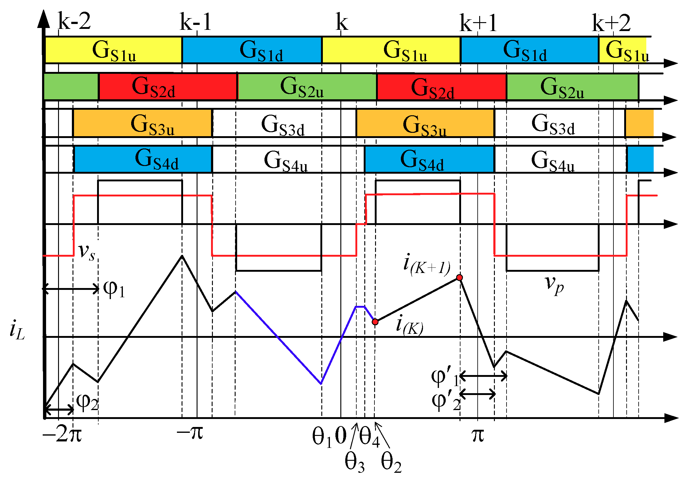
As shown in Figure 3, a step load transition happened around the reference point. In other words, the switching behaviour referring to reference point is the original steady state with phase angles , while the switching behaviour referring to (k+1)th reference point is the destination steady state with phase angles . The phase angles referring to the reference point should be selected properly to complete the transition process as fast as possible.
With the unknown , two important instant currents are calculated then:
where is the instant current at the last switching point of reference point, and is the first current at the first switching point of reference point.
To keep voltage–time balance, the average inductor current should be zero while the inductor current enter into the new steady state at once, which indicates:
Therefore, the following conditions can be obtained by substituting Equations (4), (5), (9) and (10) into (11):
It is seen that is set to zero during the interval . As shown in Equation (12), the phase shift angles and during transitions are free to be chosen. However, they should also satisfy the requirement that lets the converter work in mode A.
2.3. Load Transient Control within Mode B
In this condition, the DAB converter is working in mode B from beginning to end, and the reference points are defined in the mid of . As is shown in Figure 4, the transition is done at the reference point and the converter is expected in the destination steady state at the reference point. The instant currents after the intermediate adjustment are calculated as:
To meet such an expectation, the followed equation should be satisfied:
Combining Equations (7), (8), (13), (14) and (15), the following switching angles referring to the reference point can be calculated to achieve a fast transition within mode B:
It is seen that is set to zero during the interval . Equation (16) reveals that and can be selected flexibly. However, they should also satisfy to let the converter work in mode B.
2.4. Load Transient Control from Mode A to Mode B
In this condition, as shown in Figure 5, the phase shift angles are changed from mode A to mode B by means of the intermediate adjustment around the reference point. Different from the previous cases, the definition of switching angles are changed since that the original mode is not the same as the destination one. The instant currents after the intermediate adjustment are calculated as:
To minimize the transient period, the same requirement shown in Equation (15) should be met. Combining Equations (7), (8), (17), (18) and (15), the intermediate switching angles for transition from mode A to mode B are given as:
It is seen that is set to zero during the interval . From the results, it can be found that switching angels and can be determined flexibly. Meanwhile, the condition of mode boundary should be met too: .
2.5. Load Transient Control from Mode B to Mode A
In this condition shown in Figure 6, the original state is mode B while the final state is mode A. Therefore, the instant currents after the reference point can be calculated starting from mode B:
As the switching angles are redefined in mode A at the reference point, the requirement for the expected fast transition is the same as (11). Substituting Equations (4), (5), (20), (21) into Equation (11), switching angles during transient process referring to the reference point for the transition from mode B to mode A are:
In this case, and can be chosen flexibly, but is subject to and .
3. Validation by Experimental Results
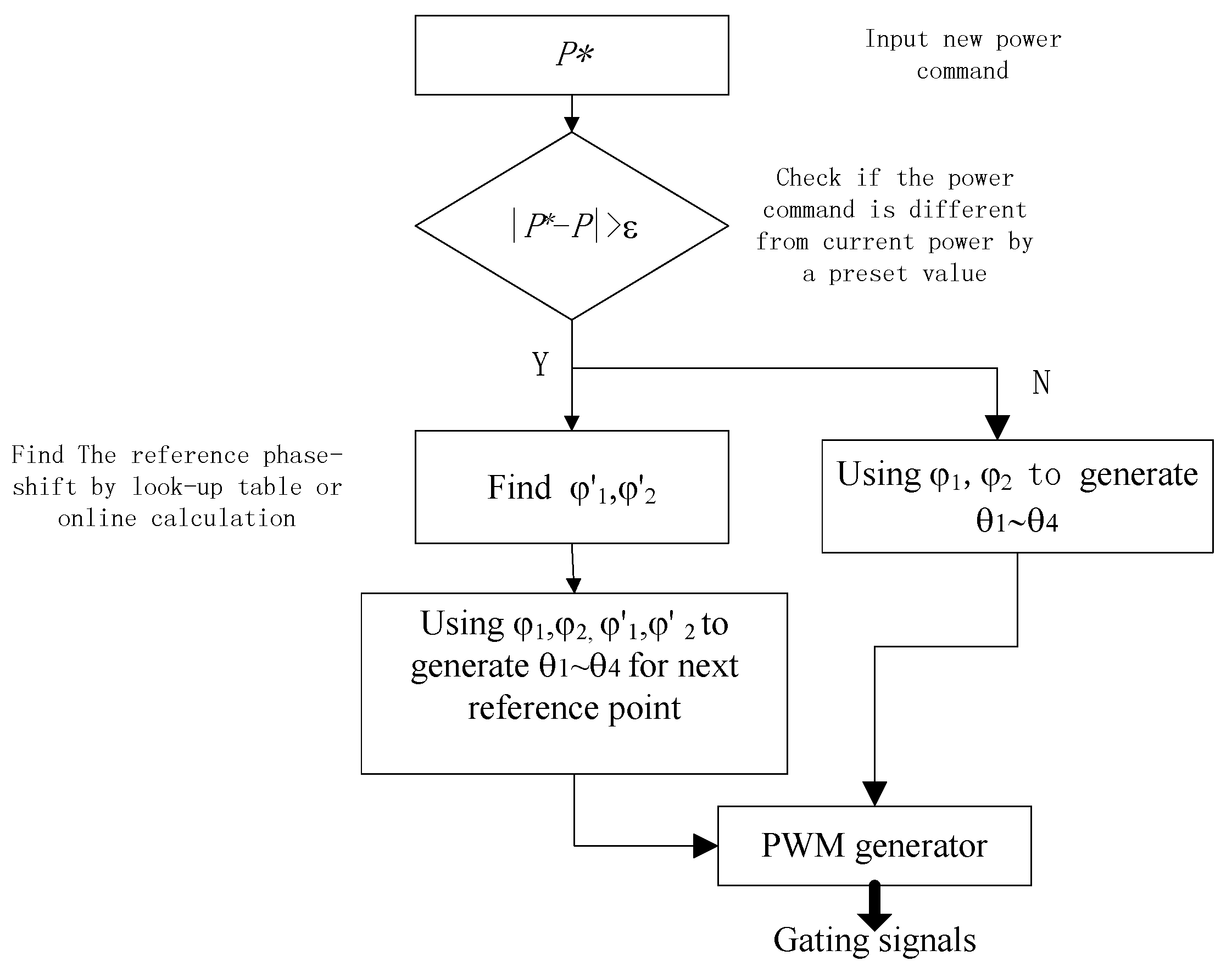
In order to validate the theoretical results, load transition cases using the proposed control method were tested on a lab prototype DAB converter. Table 2 shows the specifications of the converter used in the experiments. The circuit adopts four power MOSFETs (STP40NF20, 200 V, 40 A, 0.038 ) on the primary side and the other four power MOSFETs (IPP200N15N3G, 150 V, 50 A, 0.020 ) on the secondary side as the switches. The input terminals were connected to a DC power supply, while the output terminals were connected to a DC electronic load. The inductor is made of a toroidal CM400125 MPP core with litz wire winding. The proposed transient control is implemented in a TI-F2812 DSP development board (Texas Instruments, Dallas, USA) and the flowchart is shown in Figure 7. The converter power level is monitored continuously. If no change is to be made to the power, the current are used to generate ∼. If a new power command is received and confirmed, the destination will be calculated based on some preset algorithm optimized for better efficiency, which is out of scope of the current work. Then, for the next reference point will be updated by by using one of Equations (12), (16), (19), (22).
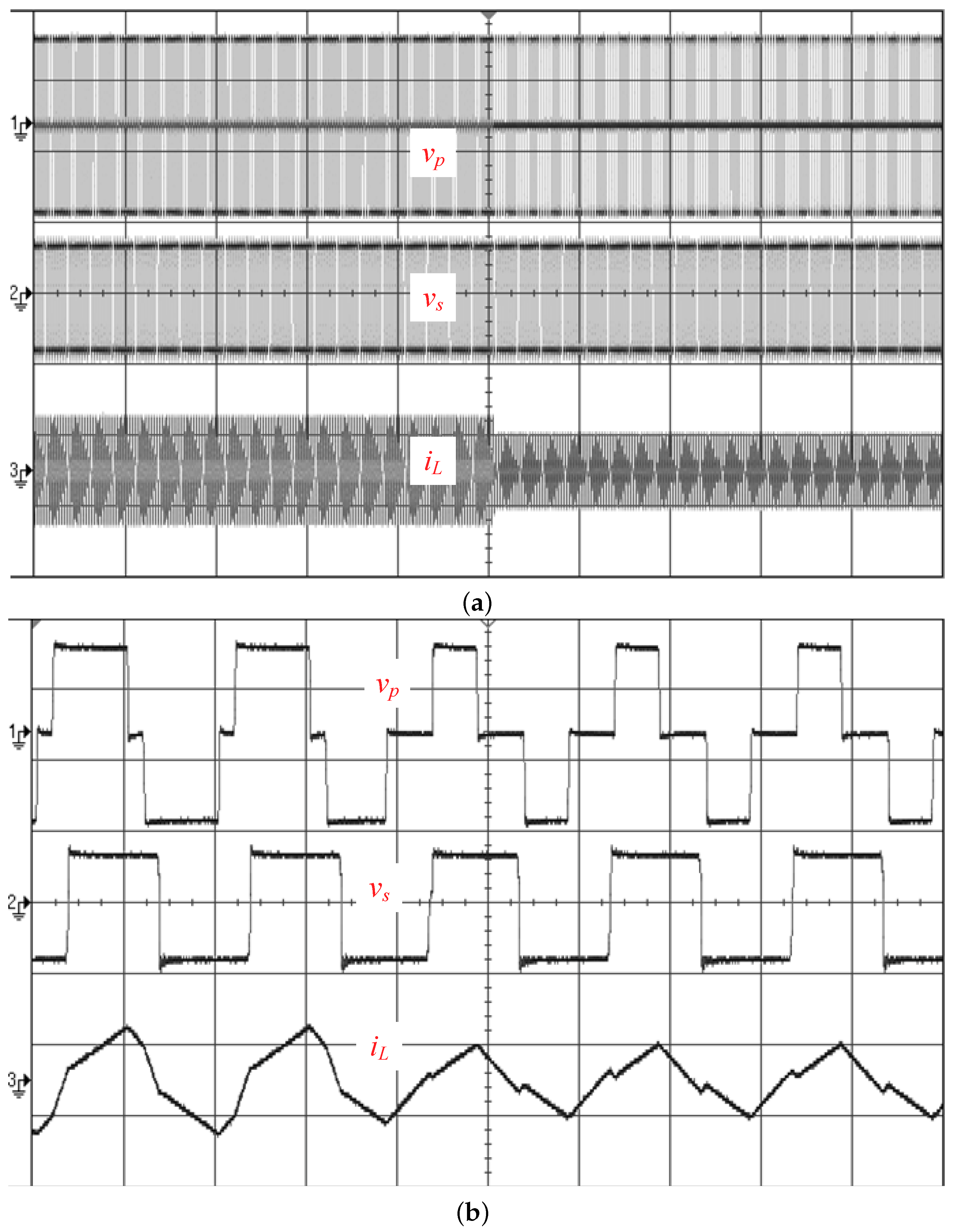
The detailed parameters of phase-shift angles of each mode in experiment are shown in Table 3, Table 4, Table 5 and Table 6. For each tested load-change condition, a condensed view of the transition is given firstly with a time scale of 300 s/div while the details are shown later with a time scale of 5 s/div. In each plot, captured waveforms of , (100 V/div) and (2 A/div) are shown from top to bottom.
As an example for comparison, the first case tested (Figure 8) is a transition within mode A by directly changing the phase-shifts. The phase-shift angles , are changed from , to , . The inductor peak current is expected to rise from 1.56 A to 2.13 A. However, an abnormal peak current 2.95 A results in a transient process and it takes about 20 HF cycles to be absorbed. In the duration of transient process, a temporal DC bias current decays from about 0.69 A until zero.
The same transition is then repeated with proposed transient control in Figure 9. According to (12), are calculated as and during the transient process. While satisfying (12), the switch angles and are selected as and during transient for the purpose of convenience. In addition, the final values of ∼ are , , and . The transient process now can be completed almost instantly as shown in Figure 9. It is seen that there is no noticeable overshoot current.
For the load transition from mode B to mode B in Figure 10, the phase-shift , are changed from , to , . After the transient modulation, the switching angles , , and are changed from , , , to , , and , respectively. During the transient process, are calculated , directly according to (16). In addition, the transient and are selected as and respectively.
In the condition of transition from mode A to mode B in Figure 11, the phase-shift , are changed from , to , . The initial angles , , and are , , , and the final angles should be , , and , respectively. At the reference point, , are determined to be and based on (19). Under the constraint given in (19), the switching angles and are selected as and , respectively, for the purpose of convenience.
In Figure 12, the condition of transition from mode B to mode A is presented, in which the phase-shift , are changed from , to , . The initial angles , , and are , , , and the final angles should be , , and , respectively. At the reference point, , are determined to be and based on (22). Under the constrain given in (22), the switch angles and are selected as and for the purpose of convenience.
4. Conclusions
In this work, a fast transient control is proposed for a DAB converter that is able to improve the step-load transient response in terms of response time and overshoot current. This transient control is implemented based on the definition of switching angles for each switch arm, which makes it easy for implementation in pulse-width-modulation (PWM) units of common micro-controller platforms. A small duration of zero-voltage is introduced in the transformer voltage during the transition process to keep the voltage-second balance of the inductor. All the transient switching angles can be calculated from the original and final phase-shift angles directly and are not affected by the converter parameters. Though the proposed control method aims to modulate the transient inductor current, no information about the instantaneous current is needed. With this proposed transient control method, the DAB converter can transfer from one steady state to another quickly and smoothly and causes no DC offset in inductor current, which has been validated successfully by a series of experimental tests.
Author Contributions
Y.Z. did most of the theoretical analysis, derivation and paper writing. C.S. contributed to circuit implementation and experimental test. X.L. is responsible for planning, coordination and proofreading. Z.H. contributed to drawing figures and formatting paper.
Funding
This work was supported by Fundo para o Desenvolvimento das Cincias e da Tecnologia under Grant No. 060/2017/A.
Conflicts of Interest
The authors declare no conflict of interest.
References
- Kheraluwala, M.H.; Gascoigne, R.; Divan, D.M.; Baumann, E. Performance characterization of a high power dual active bridge DC-to-DC converter. IEEE Trans. Ind. Appl. 1992, 28, 1294–1301. [Google Scholar] [CrossRef]
- De Doncker, R.W.; Divan, D.M.; Kheraluwala, M.H. A three-phase soft-switched high-power-density DC/DC converter for high-power applications. IEEE Trans. Ind. Appl. 1991, 27, 63–73. [Google Scholar] [CrossRef]
- Huang, J.; Wang, Y.; Li, Z.; Lei, W. Unified triple-phase-shift control to minimize current stress and achieve full soft-switching of isolated bidirectional DC–DC converter. IEEE Trans. Ind. Electron. 2016, 63, 4169–4179. [Google Scholar] [CrossRef]
- Wu, K.; de Silva, C.W.; Dunford, W.G. Stability analysis of isolated bidirectional dual active full-bridge DC–DC converter with triple phase-shift control. IEEE Trans. Power Electron. 2012, 27, 2007–2017. [Google Scholar] [CrossRef]
- Moonem, M.A.; Pechacek, C.L.; Hernandez, R.; Krishnaswami, H. Analysis of a multilevel dual active bridge (ML-DAB) DC–DC converter using symmetric modulation. Electronics 2015, 4, 239–260. [Google Scholar] [CrossRef]
- Khan, M.A.; Zeb, K.; Sathishkumar, P.; Ali, M.U.; Uddin, W.; Hussian, S.; Ishfaq, M.; Khan, I.; Cho, H.-G.; Kim, H.-J. A Novel Supercapacitor/Lithium-Ion Hybrid Energy System with a Fuzzy Logic-Controlled Fast Charging and Intelligent Energy Management System. Electronics 2018, 7, 63. [Google Scholar] [CrossRef]
- Wang, Y.-C.; Ni, F.-M.; Lee, T.-L. Hybrid Modulation of Bidirectional Three-Phase Dual-Active-Bridge DC Converters for Electric Vehicles. Energies 2016, 9, 492. [Google Scholar] [CrossRef]
- Zhao, B.; Song, Q.; Liu, W.; Sun, Y. Overview of dual-active-bridge isolated bidirectional DC–DC converter for high-frequency-link power-conversion system. IEEE Trans. Power Electron. 2014, 29, 4091–4106. [Google Scholar] [CrossRef]
- Krismer, F.; Kolar, J. Accurate power loss model derivation of a highcurrent dual active bridge converter for an automotive application. IEEE Trans. Ind. Electron. 2010, 57, 881–891. [Google Scholar] [CrossRef]
- Oggier, G.G.; Garcia, G.O.; Oliva, A.R. Modulation strategy to operate the dual active bridge DC–DC donverter under soft switching in the whole operating range. IEEE Trans. Power Electron. 2011, 26, 1228–1236. [Google Scholar] [CrossRef]
- Zhao, B.; Yu, Q.; Sun, W. Extended-phase-shift control of isolated bidi-rectional DC–DC converter for power distribution in microgrid. IEEE Trans. Power Electron. 2012, 27, 4667–4680. [Google Scholar] [CrossRef]
- Jain, A.K.; Ayyanar, R. PWM control of dual active bridge: Comprehensive analysis and experimental verification. IEEE Trans. Power Electron. 2011, 26, 1215–1227. [Google Scholar] [CrossRef]
- Bai, H.; Mi, C. Eliminate reactive power and increase system efficiency of isolated bidirectional dual-active-bridge DC–DC converters using novel dual- phase-shift control. IEEE Trans. Power Electron. 2008, 23, 2905–2914. [Google Scholar] [CrossRef]
- Zhao, B.; Song, Q.; Liu, W. Efficiency characterization and optimization of isolated bidirectional DC–DC converter based on dual-phase-shift control for DC distribution application. IEEE Trans. Power Electron. 2013, 28, 1711–1727. [Google Scholar] [CrossRef]
- Ortiz, G.; Fassler, L.; Kolar, J.W.; Apeldoorn, O. Flux Balancing of Isolation Transformers and Application of “The Magnetic Ear” for Closed-Loop Volt-Second Compensation. IEEE Trans. Power Electron. 2014, 29, 4078–4090. [Google Scholar] [CrossRef]
- Li, X.; Li, Y.-F. An optimized phase-shift modulation for fast transient response in a dual-active-bridge converter. IEEE Trans. Power Electron. 2014, 29, 2661–2665. [Google Scholar] [CrossRef]
- Lin, S.-T.; Li, X.; Sun, C.; Tang, Y. Fast transient control for power adjustment in a dual-active-bridge converter. Electron. Lett. 2017, 53, 1130–1132. [Google Scholar] [CrossRef]
- Sun, C.; Li, X. Fast Transient Modulation for a Step Load Change in a Dual-Active-Bridge Converter with Extended-Phase-Shift Control. Energies 2018, 11, 1569. [Google Scholar] [CrossRef]
- Zhao, B.; Song, Q.; Liu, W.; Zhao, Y. Transient DC Bias and Current Impact Effects of High-Frequency-Isolated Bidirectional DC–DC Converter in Practice. IEEE Trans. Power Electron. 2016, 31, 3203–3216. [Google Scholar] [CrossRef] [Green Version]
- Engel, S.P.; Soltau, N.; Stagge, H.; De Doncker, R.W. Dynamic and Balanced Control of Three-Phase High-Power Dual-Active Bridge DC–DC Converters in DC-Grid Applications. IEEE Trans. Power Electron. 2013, 28, 1880–1889. [Google Scholar] [CrossRef]
- Takagi, K.; Fujita, H. Dynamic Control and Performance of a Dual-Active-Bridge DC–DC Converter. IEEE Trans. Power Electr. 2017, 33, 7858–7866. [Google Scholar] [CrossRef]
Figure 1.
A dual-active-bridge DC/DC converter.

Figure 2.
Defined control timing in (a) mode A and (b) mode B.
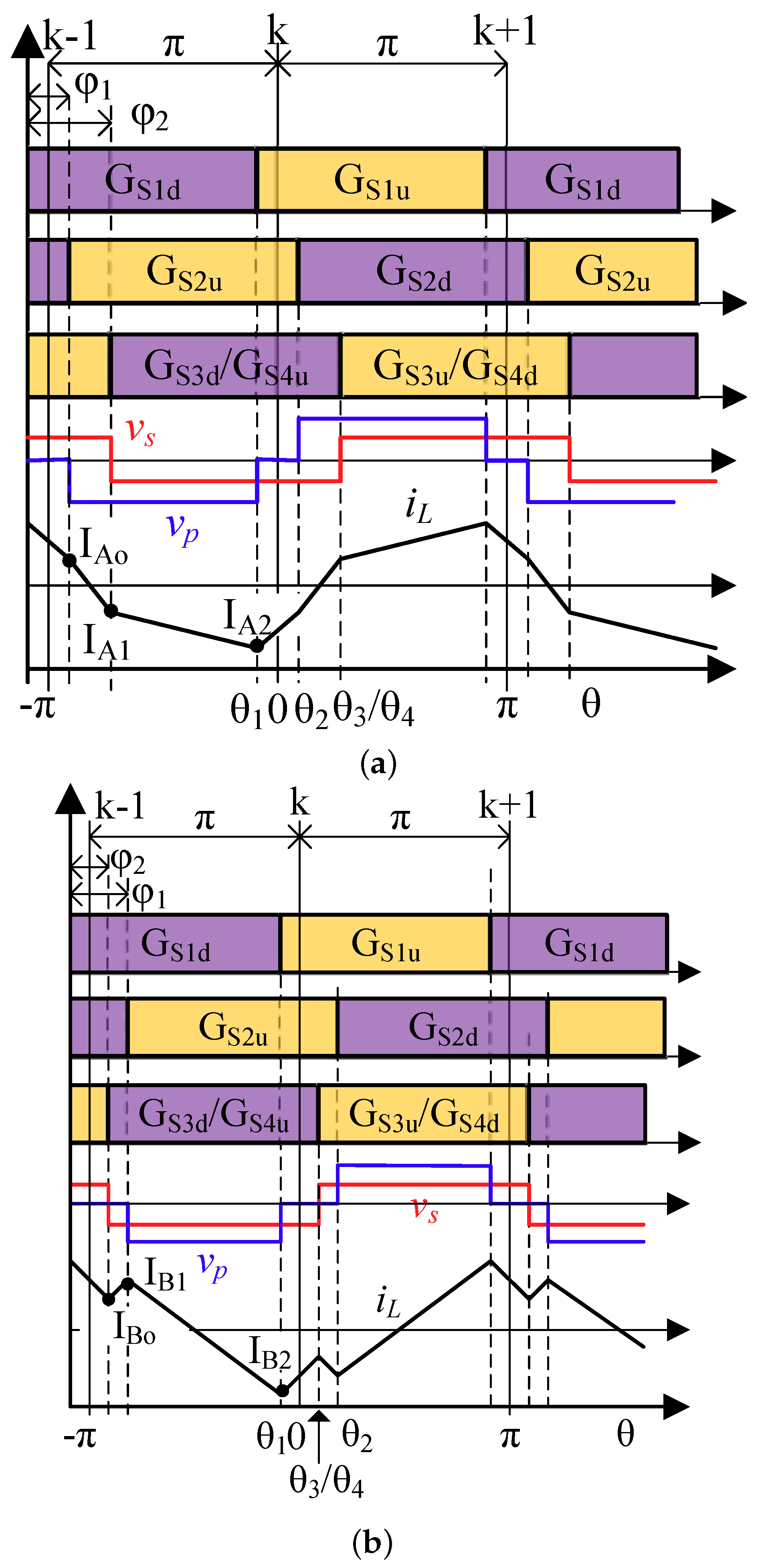
Figure 3.
Gate signals, voltage and current waveforms of transient control within mode A.
Figure 4.
Gate signals, voltage and current waveforms of the proposed control method in within mode B.
Figure 4.
Gate signals, voltage and current waveforms of the proposed control method in within mode B.

Figure 5.
Gate signal, voltage and current waveforms of the proposed control method from mode A to mode B.
Figure 5.
Gate signal, voltage and current waveforms of the proposed control method from mode A to mode B.
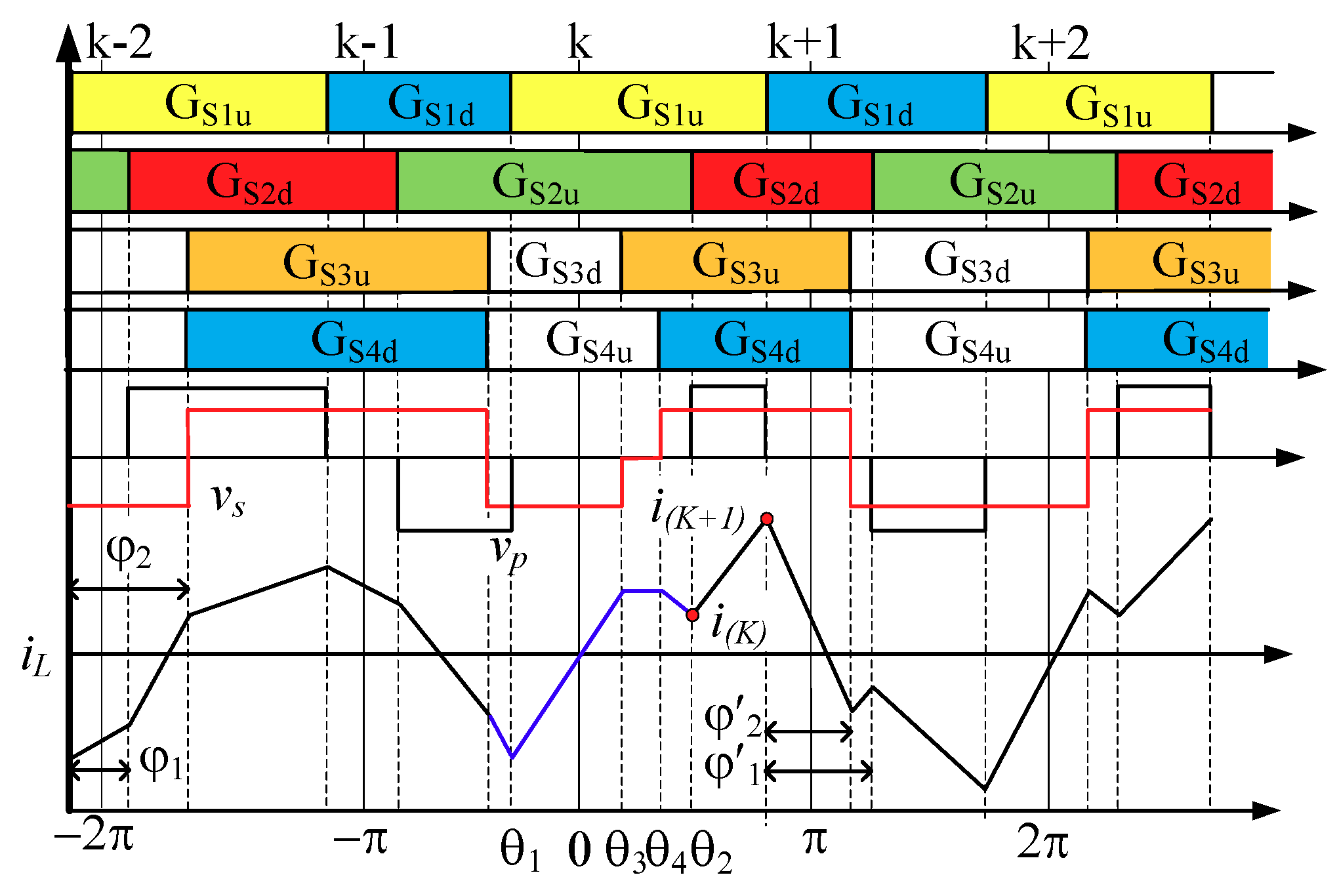
Figure 6.
Gate signal, voltage and current waveforms of the proposed control method from mode B to mode A.
Figure 6.
Gate signal, voltage and current waveforms of the proposed control method from mode B to mode A.

Figure 7.
Flowchart for implementation of the proposed transient control method.

Figure 8.
Experimental plots of transition within mode A without proposed control method. The signals shown from top to bottom are: (100 V/div), (100 V/div) and (2 A/div). (a) condensed view (300 s/div); (b) expanded view (5 s/div).
Figure 8.
Experimental plots of transition within mode A without proposed control method. The signals shown from top to bottom are: (100 V/div), (100 V/div) and (2 A/div). (a) condensed view (300 s/div); (b) expanded view (5 s/div).
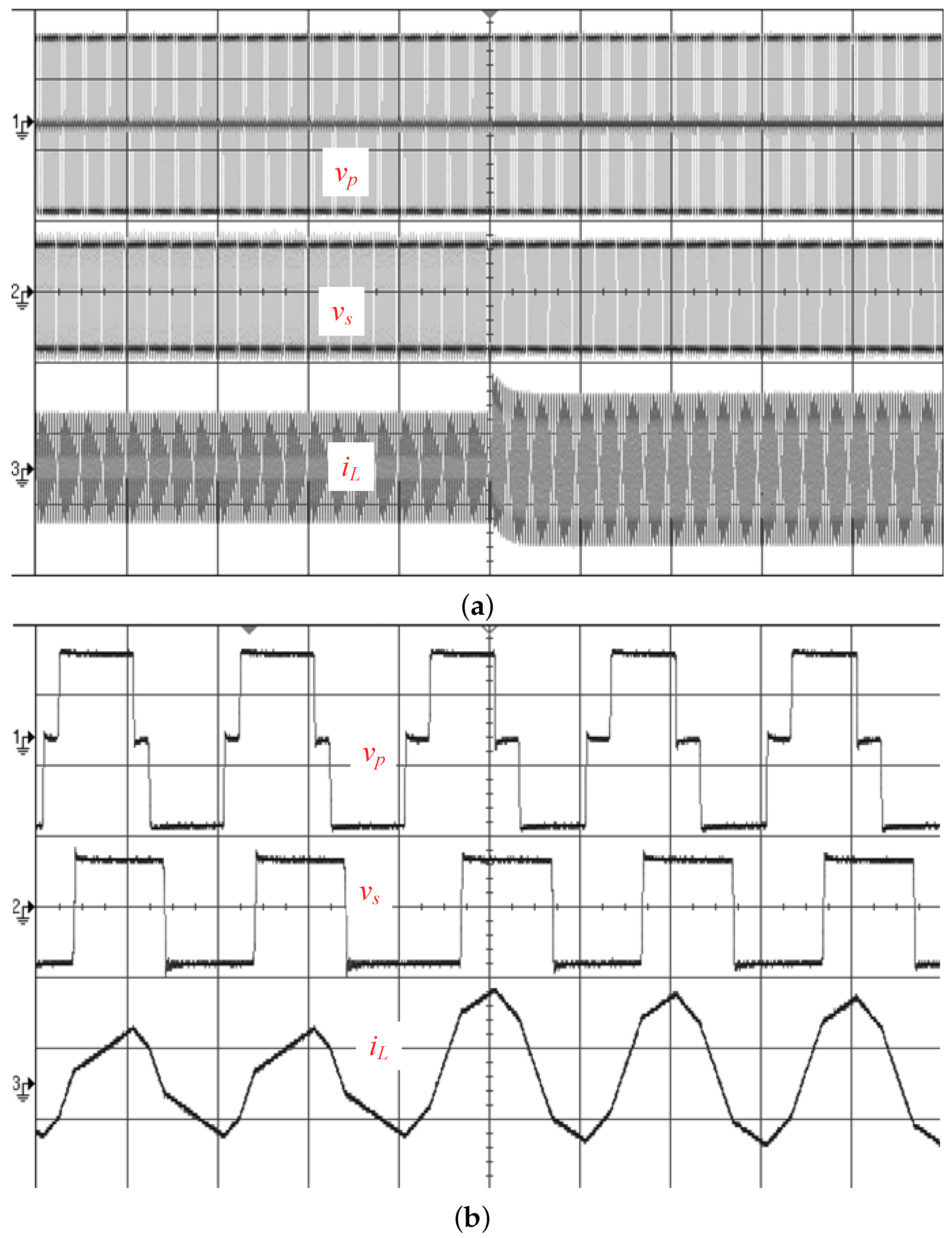
Figure 9.
Experimental plots of transition within mode A with proposed control method. The signals shown from top to bottom are: (100 V/div), (100 V/div) and (2A/div). (a) condensed view (300 s/div); (b) expanded view (5 s/div).
Figure 9.
Experimental plots of transition within mode A with proposed control method. The signals shown from top to bottom are: (100 V/div), (100 V/div) and (2A/div). (a) condensed view (300 s/div); (b) expanded view (5 s/div).
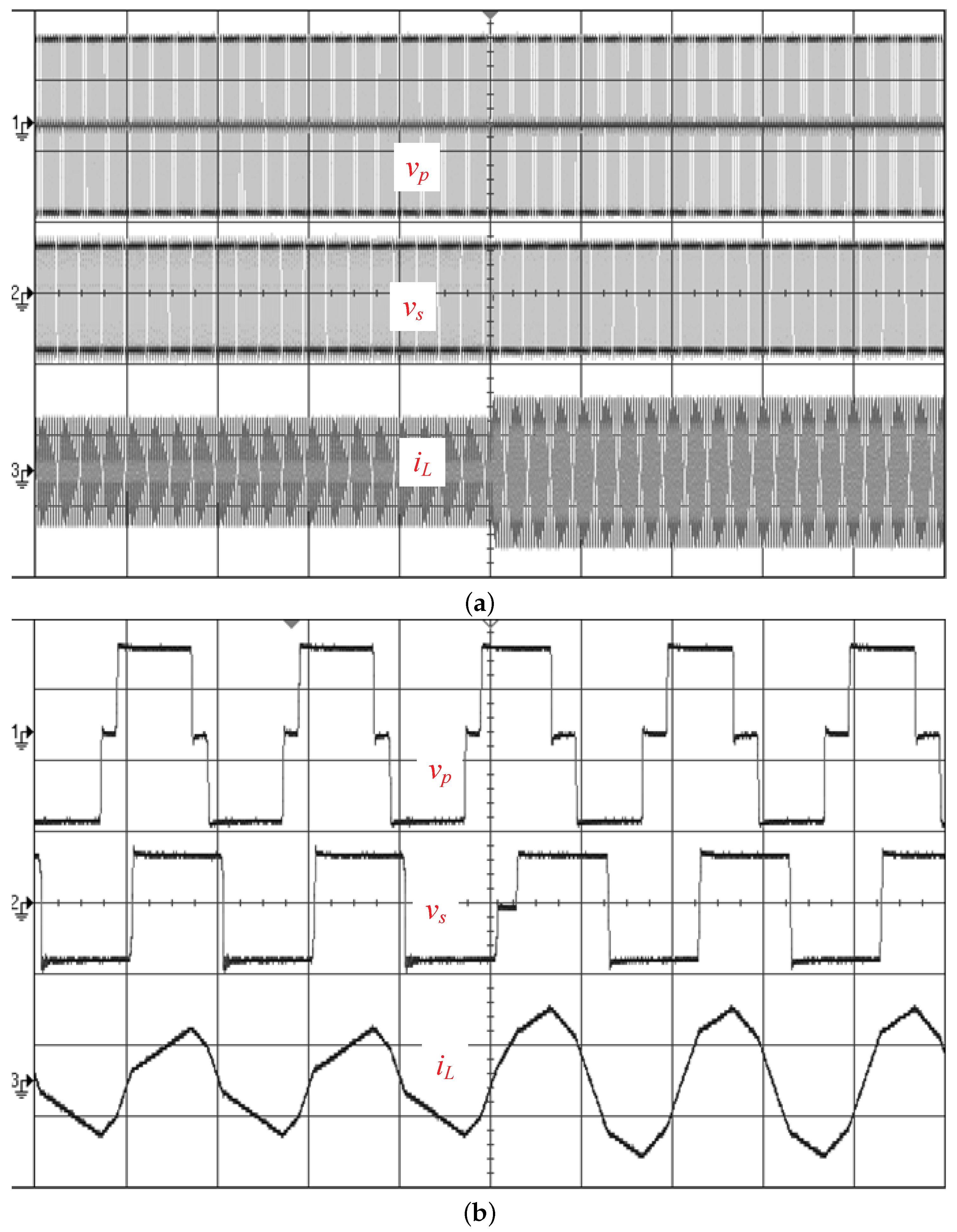
Figure 10.
Experimental plots of transition within mode B with proposed control method. The signals shown from top to bottom are: (100 V/div), (100 V/div) and (2 A/div). (a) condensed view (300 s/div); (b) expanded view (5 s/div).
Figure 10.
Experimental plots of transition within mode B with proposed control method. The signals shown from top to bottom are: (100 V/div), (100 V/div) and (2 A/div). (a) condensed view (300 s/div); (b) expanded view (5 s/div).
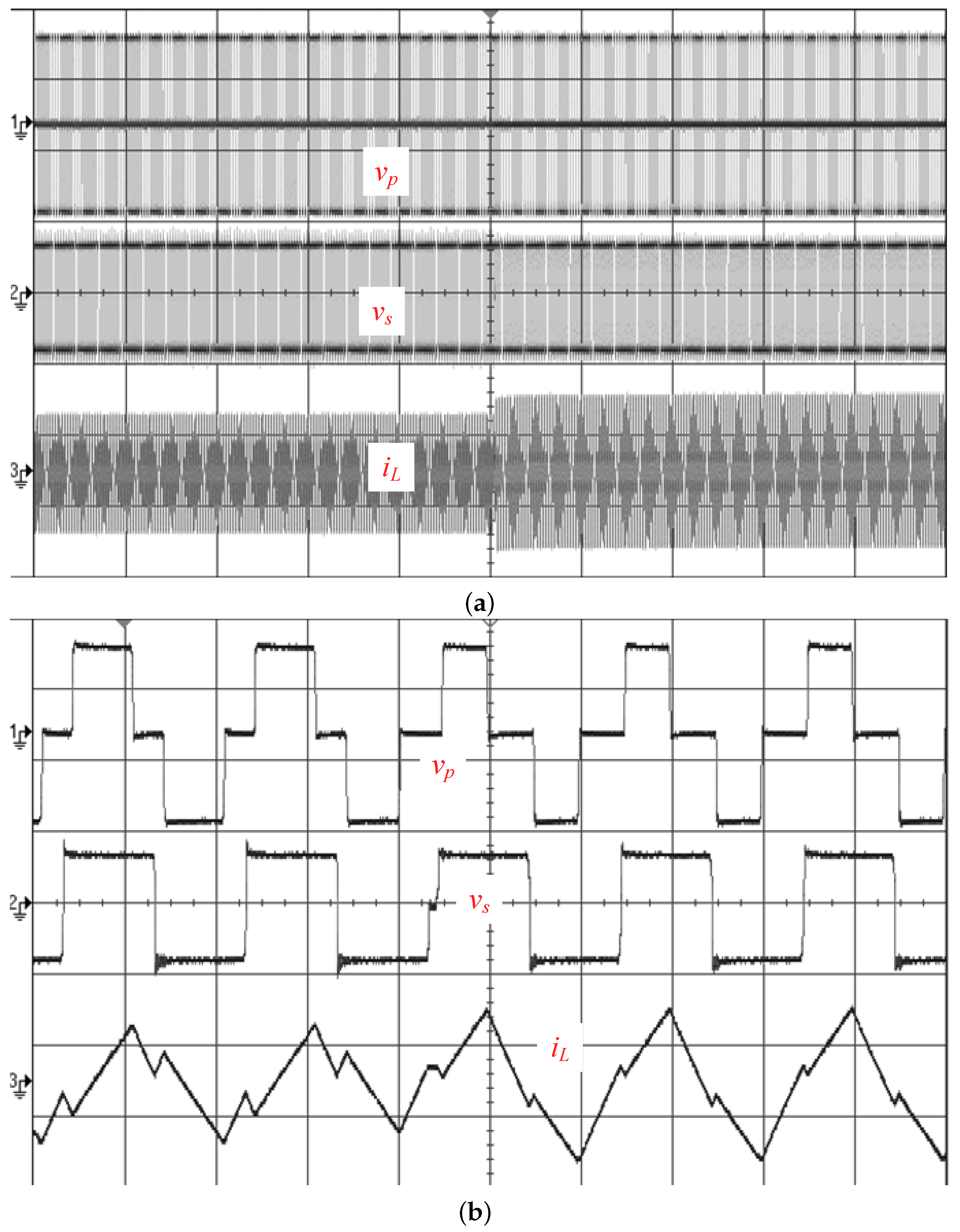
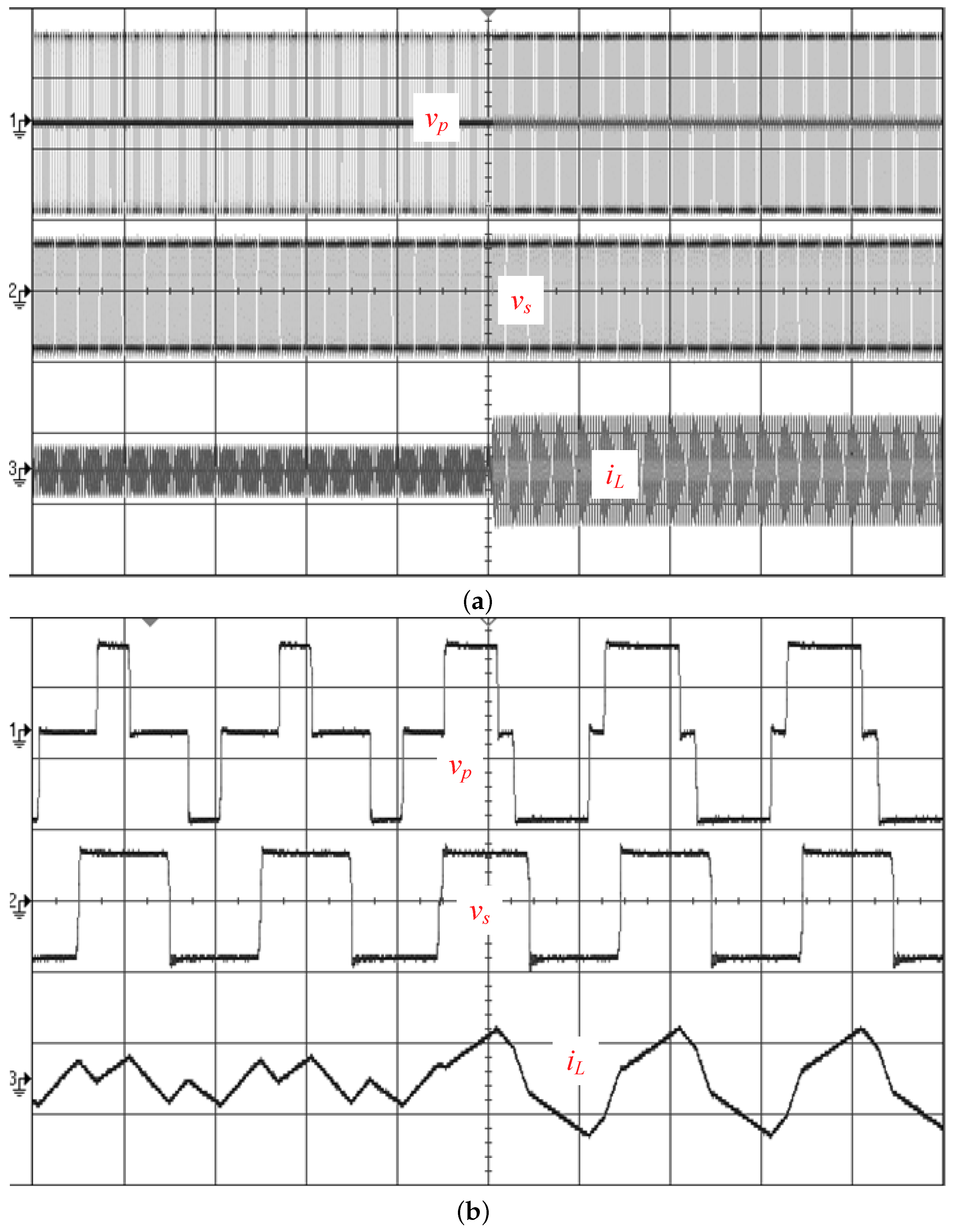
Figure 11.
Experimental plots of transition from mode A to mode B with proposed control method. The signals shown from top to bottom are: (100 V/div), (100 V/div) and (2 A/div). (a) condensed view (300 s/div); (b) expanded view (5 s/div).
Figure 11.
Experimental plots of transition from mode A to mode B with proposed control method. The signals shown from top to bottom are: (100 V/div), (100 V/div) and (2 A/div). (a) condensed view (300 s/div); (b) expanded view (5 s/div).

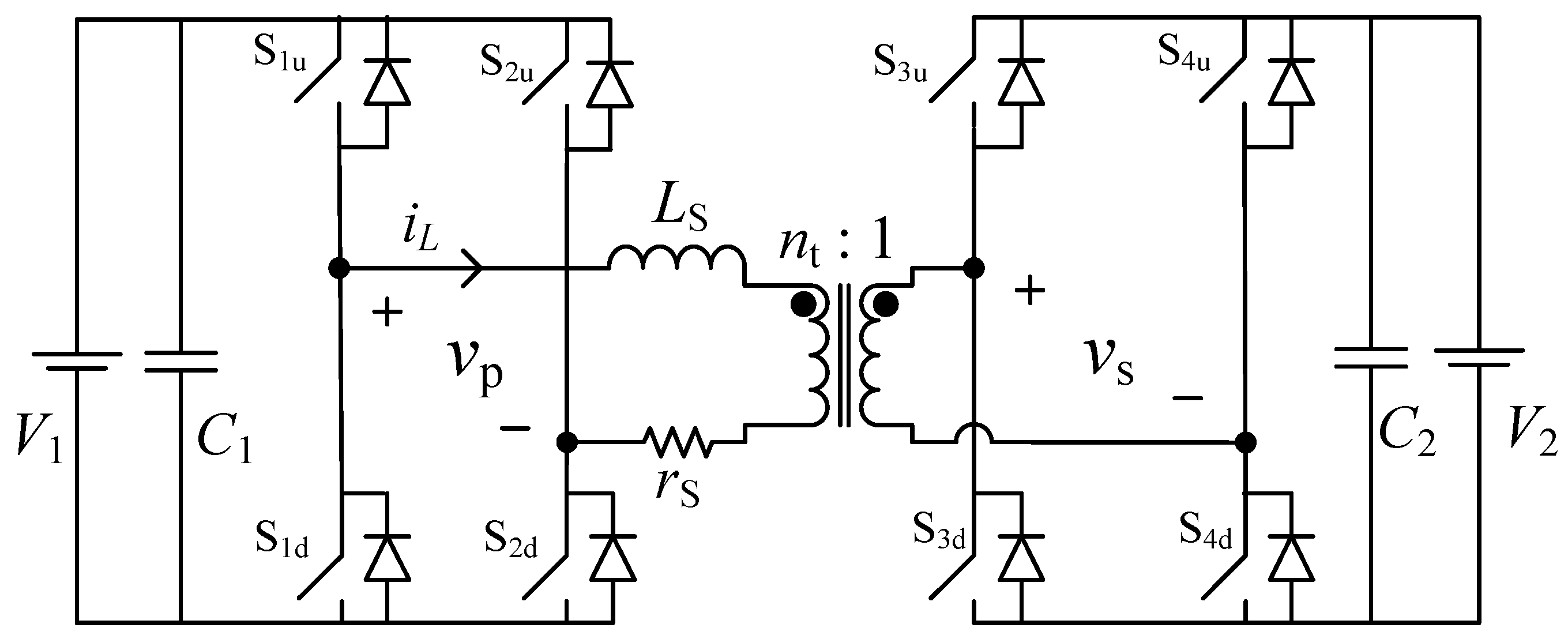
Figure 12.
Experimental plots of transition from mode B to mode A with proposed control method. The signals shown from top to bottom are: (100 V/div), (100 V/div) and (2 A/div). (a) condensed view (300 s/div); (b) expanded view (5 s/div).
Figure 12.
Experimental plots of transition from mode B to mode A with proposed control method. The signals shown from top to bottom are: (100 V/div), (100 V/div) and (2 A/div). (a) condensed view (300 s/div); (b) expanded view (5 s/div).

Table 1.
Different load transition conditions of EPS control.
| Initial Mode | Final Mode | |
|---|---|---|
| Condition 1 | Mode A | Mode A |
| Condition 2 | Mode A | Mode B |
| Condition 3 | Mode B | Mode B |
| Condition 4 | Mode B | Mode A |
Table 2.
Specifications of the prototype converter.
| Parameters | Value |
|---|---|
| DC input voltage | 120 V |
| DC output voltage | 72 V |
| Transformer turns ratio | 1:1 |
| Transformer ferrite core | PC40ETD49 |
| Series inductor | 121.875 H |
| HF filter capacitance , | 330 F |
| Primary-side MOSFETs | STP40NF20 |
| Secondary-side MOSFETs | IPP200N15N3G |
| Switching frequency | 100 kHz |
MOSFET: metal-oxide-semiconductor field-effect transistor
Table 3.
Transition within mode A.
| Phase-Shift-Angles | Initial | Transient | Final |
|---|---|---|---|
Table 4.
Transition within mode B.
| Phase-Shift-Angles | Initial | Transient | Final |
|---|---|---|---|
Table 5.
Transition from mode A to mode B.
| Phase-Shift-Angles | Initial | Transient | Final |
|---|---|---|---|
Table 6.
Transition from mode B to mode A.
| Phase-Shift-Angles | Initial | Transient | Final |
|---|---|---|---|
© 2018 by the authors. Licensee MDPI, Basel, Switzerland. This article is an open access article distributed under the terms and conditions of the Creative Commons Attribution (CC BY) license (http://creativecommons.org/licenses/by/4.0/).
Share and Cite
MDPI and ACS Style
Zhang, Y.; Li, X.; Sun, C.; He, Z. Improved Step Load Response of a Dual-Active-Bridge DC–DC Converter. Electronics 2018, 7, 185. https://doi.org/10.3390/electronics7090185
AMA Style
Zhang Y, Li X, Sun C, He Z. Improved Step Load Response of a Dual-Active-Bridge DC–DC Converter. Electronics. 2018; 7(9):185. https://doi.org/10.3390/electronics7090185
Chicago/Turabian StyleZhang, Yifan, Xiaodong Li, Chuan Sun, and Zhanhong He. 2018. "Improved Step Load Response of a Dual-Active-Bridge DC–DC Converter" Electronics 7, no. 9: 185. https://doi.org/10.3390/electronics7090185
Note that from the first issue of 2016, this journal uses article numbers instead of page numbers. See further details here.