1. Introduction
The tremendous demand for smart weapons and stronger military systems along with the emergence of cyber terrorism as well as electronic and information warfare have changed the design requirements for military-related electronic sensors and systems. Nowadays, the radical extremists and adversaries try to cyber murder and kill these systems at software- and/or hardware-level and perform malign black operations, such as cyber espionage, subverting the routing path and targeting point of a launched missile or sabotaging the manufacturing process of chemical, biological, radiological, and nuclear (CBRN) weapons. The architect and/or sergeant of an attack can be an insider traitor or outsider criminal, and his/her position can be in any stage of the software and/or hardware design and development. In this regard, the defense companies are required to provide the missiles, the aircraft fighters, and any other military-related products with the highest level of safety and quality standards [
1,
2,
3,
4,
5,
6]. In order to satisfy this demand, different methods for quality checking, management, and control of products at multiple stages of manufacturing and usage processes are employed. Common methods in this aspect are: (a) statistical processing control, which is a system for monitoring and inspecting the status of a process, revealing any tendency for the process to leave the prescribed norms, and allowing corrective actions to be taken before the product is affected; (b) using a reliability, availability, and maintainability-based computer aided design (RAM-based CAD) system to assist in the design of circuits; (c) using a vendor rating system that acquires certain data from the incoming inspection, the survey results performed by a vendor quality group, and the line rejects that are discovered during assembly and test; (d) protecting products through physical and/or electronic labeling and using track-and-trace software to reduce the time and cost of recalls, and take proactive steps to prevent recalls; and (e) leveraging legal and governmental agreements between the trading partners.
However, the defense electronics industry constantly struggles to provide the latest quality standards and updated methods to the government agencies and companies due to the increasingly complex defense requirements, emergence of new technology generations, creation of new electronic warfare threats, ever cyber threats at software- and hardware-level, and aging of published specifications and standards for monitoring and inspecting the products. Also, any of the discussed methods for quality checking, management, and control of products may be compromised physically or virtually by a malicious person. Therefore, it is mandatory to security check these electronic systems in a bottom-up (or top-down) approach and equip it with an iron dome that can locate the virulent software/hardware component, hold it in custody, and provide protection. This work focuses on the security of these electronic systems at hardware-level. The modern electronic equipment in military applications presents system designers with an essential contrast between: (1) the real world observed and understood by human beings through radar systems along with the other radio frequency (RF) sensor applications using analog information; and (2) the information processing environment (such as automatic target recognition system or pistol grip pattern recognition system) [
7,
8,
9,
10]. In this regard, an interface is required for translation of the analog information in the real world into the digital data for processing and vice versa. This data conversion links the analog world to the digital world. Without this interface, most of the data processing elements in the RF-related applications such as radar, software-defined radio, electronic warfare, missile guidance, high-end test and measurement devices, and counter improvised explosive device systems would be useless and development of analog processors with their possibly complicated and expensive designs would be necessary. Therefore, this hybrid data processing sets a necessitation on their main processing core to include and carry out both analog and digital functions on the chip. These functions are realized by mixed-signal integrated circuits (ICs). The mixed-signal ICs usually adopt the system-on-chip (SoC) technique as their design principle for acceleration of their design-to-usage process. According to this technique, the IC designer (or SoC integrator) builds and implements a specified main function and its circuit through forming the essential interconnections between the delivered analog and digital intellectual property (IP) cores (or sub-circuits) by third parties (external sources).
The catered IP cores by unknown external sources in the diverse environment of the semiconductor supply chain may not be trustworthy. It is probable for a core to render an alternative function due to an applied malicious change to its circuit that is known as a Hardware Trojan (HT). A Trojan should be activated by a rare event (to be sneaky) and it can be designed and inserted during design or fabrication processes by untrusted people (third party IP provider, SoC integrator, or foundry employees), design tools, or modules. Hardware Trojans can create catastrophic and life-threatening situations in military systems such as misguiding the defensive/offensive mechanisms or deviating the transmitted secret information from a trusted to a malign communication channel. In this work, we consider a scenario in which the SoC integrator is the backstabber and attempts to victimize analog and/or digital IP cores by creating a Trojan within the chip through an adaptive mechanism [
11,
12]. Due to the importance and critical role of signal converters (or the conversion interface) in mixed-signal ICs, they can be a target for manipulation and demolition by adversaries. An adversary may launch different attacks on these electronic modules such as HT insertion. The countermeasures for Hardware Trojan attack are divided into three groups: (a) Trojan detection (such as side channel analysis, reference comparison, increasing controllability and observability, and reverse engineering); (b) design for security (such as preventing insertion and facilitating detection); and (c) monitoring and testing the system functionality externally and/or internally, which is known as built-in-self-test (BIST) [
13,
14].
According to the BIST, a part of an IC chip (or new added analog and/or digital cells) is used to test and verify the chip partly or entirely according to the received response. Depending on the chip operational condition, the BIST is classified as online or offline. In the online BIST, integrity testing and security verification occur during the active/idle mode of the normal circuit operational state. In the offline BIST, there is a certain operational state for testing and verifying the chip. There are differences when these approaches are utilized to test and verify security of digital circuits or analog/mixed-signal circuits. For example, the input data for testing digital circuits has logical (binary) nature while it can be either a continuous analog signal or a digital pattern for mixed-signal circuits. We define the BIST module as the central intelligence unit (CIU) in the hardware security terminology. Many research works were done for security checking and protection provision in the digital domain [
11,
12], while only a few studies are seen in the analog/mixed-signal domain [
15,
16,
17,
18,
19,
20,
21]. Due to this lack of knowledge, more research needs to be done in the area of analog/mixed-signal hardware security in order to find and develop related threats and countermeasures. In this regard, our work targets the security evaluation of delta sigma (
) analog to digital converter (ADC).
The contributions of this paper can be stated as: (1) studying a first-order one-bit
ADC from the security perspective; (2) proposing four mixed-signal threat models for the ADC; (3) proposing a CIU mechanism for security checking and defending the ADC; and (4) analysis of the ADC functionality under the proposed threats and countermeasure.
Section 2 explains the contributions in detail. The results, analysis, and discussion are presented in
Section 3. Conclusion is given in
Section 4.
2. Threat Models and Countermeasures for a Delta-Sigma ADC
The communications and signals within the military area include all aspects of communications, interactions, and conveyance of information between armed forces and the respective electronic devices. They can be in various forms such as voice and audio signals, tactical ground-based communications, terrestrial microwave signals, satellite signals, signals of mobile devices, and jamming signals. Most of these signals have analog nature and should be transformed into the digital domain in order to employ them in different computing processes. In this way, their processing, transmission, and storage are facilitated. The process of converting an analog signal to binary data (which is a number of codes or a series of ones and zeros) is called quantization, and the electronic device that executes this function is called analog to digital converter. The ADC resolution (not necessarily its number of output bits) determines the number of quantization levels that can partition a voltage range. The functionality correctness and integrity of an ADC is highly critical since it has direct impact on the reconstructed analog signal from the ADC output. An ADC functionality is approved if: (a) there is mapping from the analog input signal to the digital output without introducing significant quantization errors; and (b) the quantization levels are usually equally spaced, except in non-linear ADCs. In this situation, even infrequent (and unintentional) functionality failure(s) can have a detrimental effect on the system operation. Therefore, it is necessary to test the ADC functionality to avoid any failure.
There are four metrics for classification of ADCs for different applications: sampling rate, resolution, noise and distortion rejection/attenuation, and physical footprints (area and power consumption). The two most popular types of ADCs are successive approximation register (SAR) ADC and ADC. The SAR ADCs provide an acceptable resolution, low power dissipation, and relatively high sampling rate, while the ADCs deliver very high resolution at lower sampling rate. The SAR ADCs are employed for general purpose applications (such as data loggers, temperature sensors, and bridge sensors), while the ADCs are utilized in specific purpose applications (such as wireless and line communications, test and measurement instrumentation medical imaging, radar systems, electronic warfare, unmanned vehicles, and missile systems). With respect to this classification, we study the security of analog to digital converter. An ADC can be infected by insertion of an HT inside the chip, with the payload of causing an intentional error during the ADC operation. In this work, the ADC functionality failure is chosen as the payload for Hardware Trojan design that induces rare but harmful effects in the system operation, such as miscalculation and inaccuracy of a smart weapon in tracking and pointing at the targeted point or disabling the weapon scope completely.
Now, we discuss a first-order one-bit
analog to digital converter that is used in our security analysis. The chosen configuration for the ADC is because of its simplicity for implementation. The
modulator circuit is implemented using AlGaSb/InAs tunnel field effect transistor (TFET) technology, provided in the Universal TFET model 1.6.8 [
22]. The TFET device with the 20 nm technology node is suitable for low power applications and provides area efficiency. The Universal TFET model is a simple and versatile semi-empirical, physics-based, Simulation Program with Integrated Circuit Emphasis (SPICE)-friendly, analytical, closed-form compact model based on the Kane-Sze formula that describes the current-voltage characteristics of TFETs using a simple, continuous, and large-signal equation set [
23,
24]. Its formulation does not rely on any specific TFET embodiment and is widely configurable due to describing only the fundamental physics of the generic device. The model takes the unique features of the device, including the decrease in subthreshold swing with drain current and the superlinear onset of the output characteristic. Also, it captures the ambipolar current characteristic at negative gate–source bias and the negative differential resistance for negative drain–source biases. Its reasonably general validity, not being specific to a particular geometry, and the shown current-voltage characteristics make it a good candidate for circuit simulation, comparable to the metal–oxide–semiconductor field-effect transistor (MOSFET) SPICE models. Other TFET models usually focus on particular TFET gate configurations, or on specific aspects of the transport. Consequently, the resulting expressions for the drain current are complex and it is possible there may not be intuitive connection to the device physics.
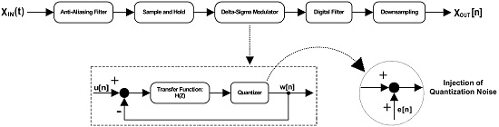
The top-level architecture of a
ADC along with a general model for the delta-sigma modulator are shown in
Figure 1. This architecture consists of five main blocks: (1) anti-aliasing filter, which is required to band-limit the input signal to frequencies less than one-half the oversampling frequency. Implementation of this filter can be quite simple, such as a simple resistor–capacitor (RC) low-pass filter, when the oversampling ratio is large; (2) sample and hold, which is responsible for sampling the signal under process; (3) delta-sigma modulator, which converts the analog signal into a noise-shaped but low resolution digital signal; (4) digital filter, which is a low-pass filter for eliminating (or attenuating) noise and increasing resolution; and (5) down-sampling, which lowers the signal sampling frequency to usually equal twice the frequency of the desired bandwidth of the input signal. Meanwhile, some of these blocks can be combined or extended depending on the circuit implementation.
and
are the analog input signal and the digital output signal of the
ADC respectively.
It is assumed that the converter has a multiplex-based input mechanism (not shown in the figure). Therefore, there are two options for the analog input signal: (A) an external single-ended analog signal, which comes from the outside world. It can be acquired using a sensor through measuring a physical quantity of an object in single-ended mode; and (B) a standard analog signal for testing the ADC generated by the CIU (or an intelligence inquiry by the CIU) internally. This signal should have a fit waveform (such as sinusoidal, triangular, and sawtooth), frequency (or period), and amplitude. Depending on the status of an “Intelligence Mode” signal, a decision is made on sending either option “A” or option “B” to the anti-aliasing filter block. For example, if this selection signal is equal to logic one, then the analog test signal is sent to the filter block. This is beneficial for situations in which the external input signal is not standard and test-friendly, while the ADC needs to be tested and security checked. In addition, the status of the selection signal can be determined either externally by user or internally through the predefined conditions. The testing and security checking process can occur during the IC run-time operation when either the ADC is idle or it is active and the external analog input signal has a suitable waveform (such as sine) for testing.
The general linear model for the modulator is analogous to an amplifier realized by an operational amplifier (op-amp) and feedback. According to this analogy, the feedback reduces the effect of noise at the output through the closed-loop. By analysis of the signal, noise, and system transfer functions, it is realized that the system needs to have a pole at dc in order to high-pass filter the quantization noise and achieve first-order noise shaping. The pole for the system transfer function is modeled as a delay block and is implemented as an integrator at circuit-level. Meanwhile, higher order delta-sigma ADCs, with more than one stage of integration and summation (or feedback) in the modulator, can be used to achieve further noise shaping and higher resolution. , , and are the input signal, the output signal, and the error signal in the modulator system respectively.
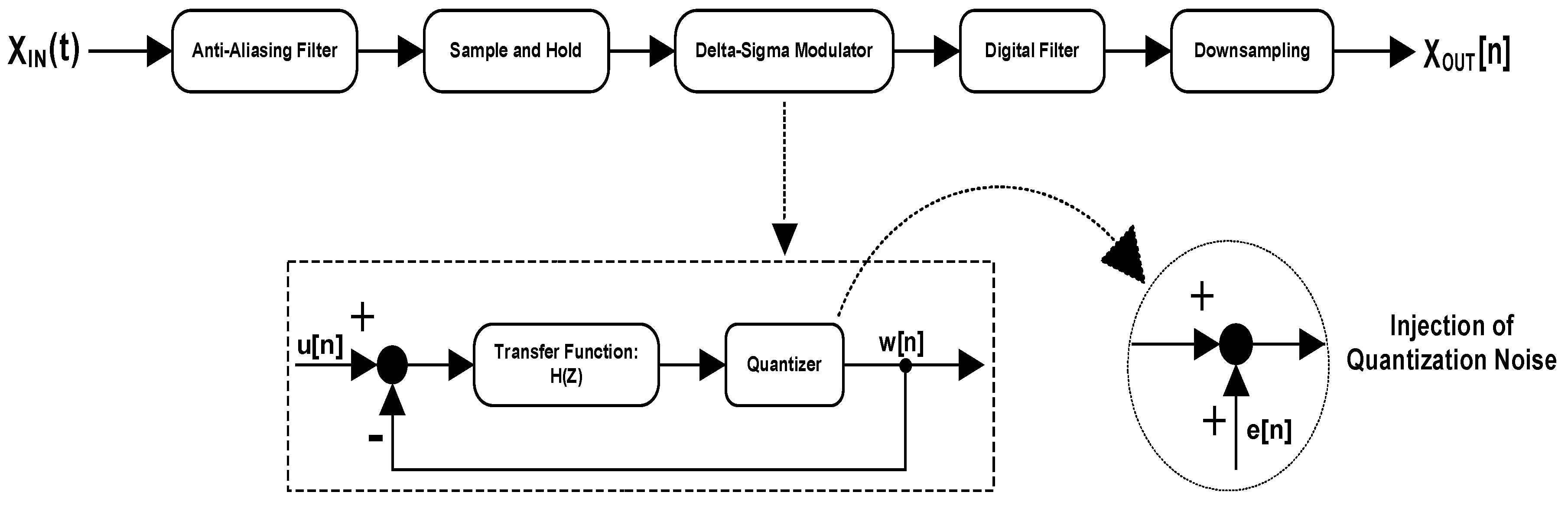
Figure 2 shows the circuit implementation of the modulator model. All the circuit elements for each component are sized through parametric simulation and analysis. It is emphasized that only “functional correctness” of the modulator was our aim during its design and implementation (since the designed Hardware Trojans have the payload of causing functionality failure). The circuit consists of five main components: (a) differential amplifier, which amplifies the difference between two input signals (
and
) but suppresses any signal common to the two inputs. The output signal (
) is ideally proportional to the difference between the two input signals. In here, an operational amplifier is used as the engine (or the main element) in building the differential amplifier. Its source supply voltage (
) is equal to the negative of the drain supply voltage (
), which means
; (b) integrator (or integrating amplifier), which accumulates the input signal over a defined time to produce a representative output signal. In other words, it performs the mathematical operation of integration on the input signal with respect to time. This amplifier has a low pass filtering effect as well (at the beginning). The operational amplifier is used to build this component (similar to the differential amplifier); (c) comparator, which compares two input signals and outputs a digital signal (whose value is between ground and supply voltage) that indicates the larger input signal. A comparator can be simply made by the op-amp. In this circuit, the negative terminal of the comparator is connected to a reference voltage (
) that is equal to
; (d) D-type flip-flop (also known as data or delay flip-flop), which captures the input signal value at a certain portion (or edge) of the clock signal (
) and outputs the value (which is between ground and supply voltage). The output signal cannot be changed at the other times; and (e) analog multiplexer, which chooses one of two analog input signals (
and
) according to the select signal (
) and sends it to the output line (
).
means the inversion of the select signal. The analog multiplexer is used as a simple digital to analog converter (DAC) in the
modulator circuit. The amplitude of DAC output signal is between negative supply voltage and positive supply voltage.
The modulator circuit operation can be described as: all the flip-flops and registers within the SoC design are reset once the chip is turned on. Therefore, the stored value in the D-type flip-flop of the modulator circuit is equal to zero at the beginning (which means ). In this case, the analog multiplexer output () is equal to . Next, is subtracted from the input signal () to the modulator using the differential amplifier. The result signal goes to the integrator. The integrated signal is compared against the reference signal (). The comparison outcome is captured by the D-type flip-flop. This process continues until the modulation process for the input signal is terminated. Conventionally, the D-type flip-flop output signal (), or the “modulator output bit”, is sent directly to the digital filter block for processing. In this work, we can consider two variations in this flow for processing and security checking of the modulator output. Case 1: the central intelligence unit is in parallel with the digital filter in the ADC architecture. The modulator output bit () is sent to the digital filter for processing, while the “modulator output signal” or the DAC output signal () is sent to the CIU for security checking. In this case, if the DAC output signal is reported as suspicious, further processing the modulator output bit is stopped and the user is notified. Case 2: the central intelligence unit is in series between the modulator and the digital filter. The DAC output signal () is sent to the CIU for processing and security checking. In this case, the CIU filters the intentional (and unintentional) fluctuations within the signal and makes a decision on the trust and validity of the result signal depending on its quality and closeness to the reference (golden) signal. If it is malicious, further signal processing is stopped and the user is notified. Otherwise, the signal is simply converted to digital format and is sent to the digital filter block. The advantage of sending the DAC output signal (instead of the modulator output bit) to the CIU is: (i) reducing the possibility of having undiscovered malicious manipulation at the DAC output signal; and (ii) requiring an analog filter that has the benefits of less circuitry, less area and power consumption, easier signal debugging under processing, higher accuracy (sometimes), fine-grained signal processing, less bandwidth demand, and being able to process large signals while causing noticeable distortion and aliasing (in comparison with its digital filter counterpart).
An attack on a system functionality has more disastrous outcomes in comparison with the other types of attacks, such as information leakage or performance degradation. In this regard, a malicious SoC integrator can design a Hardware Trojan with the goal of causing the
ADC malfunction “sometimes” through manipulating the input signal, the output signal, or the output bit of the modulator. It is assumed that the designed function-targeting Hardware Trojans are not detected during the testing and verification phase since the “Mate Trigger” for the “Main Trigger” of each Hardware Trojan is generated by other parts of the SoC during the “chip run-time operation”. In other words, the mate trigger and the main trigger for each Trojan go to an AND function before being applied to the Trojan payload circuit. Meanwhile, the main trigger mechanism of each Trojan circuit is designed based on the principle of making its activation “random” and “sneaky”. The catered simulation results in
Section 3 are obtained based on activating the Trojans using only their designed “Main Triggers” and the scenario of having “Mate Triggers” is not applied in these simulations. Without considering this scenario, the Trojans are not sneaky enough in terms of activation time and caused changes in the circuit functionality that are considered as limitations. By taking the scenario into account, the function-targeting Hardware Trojans are possibly not detected during the testing phase since there is no knowledge about the application that is going to be run on the chip. Therefore, there is less controllability and observability on the Trojan circuits and they behave more covertly. The payload of these Trojans is manipulating the input signal or the output signal/bit of the modulator circuit. This manipulation can be justified based on five different plots: (a) doing manipulation based on the internal circuit states for leakage of information; (b) occurrence of functionality failure, which is the case in this work due to its easier modeling and simulation for demonstration; (c) doing manipulation for revealing circuit activities and/or structure; (d) jeopardizing the security mechanisms of the related applications that rely on a trustworthy interface for analog to digital conversion of information; and (e) doing mild manipulation of signals for the purpose of sign communication between two entities that participate in executing an attack. A countermeasure is proposed for the designed Hardware Trojans that attempt to eliminate their payloads through signal filtering. With respect to implementing each of the proposed Hardware Trojans, its number of analog and/or digital cells may be reasonable compared to the total number of cells used in a system on chip. Also, we can consider a scenario for Hardware Trojan implementation according to which the idle cells (or the time-based unused cells) of the SoC chip are detected and employed adaptively in order to construct the Trojan functionality. In addition, hardware obfuscation may reduce the possibility of detecting the Trojans through physical inspection. The shown area overheads for the Trojans in
Section 3 are calculated, considering the insertion of “extra” cells for implementing the Trojans. Without the discussed scenario, these Trojans have limitations in terms of the added circuitry. The same concept may be applied for the defense hardware implementation. Meanwhile, it is assumed that the contribution of the defense hardware to the total chip area, performance, and power consumption will not be significant, considering all the blocks in the
ADC (not only the modulator) along with the nearly small portion that it occupies in a system-on-chip design [
25,
26].
2.1. Attack 1: Input Signal Manipulation
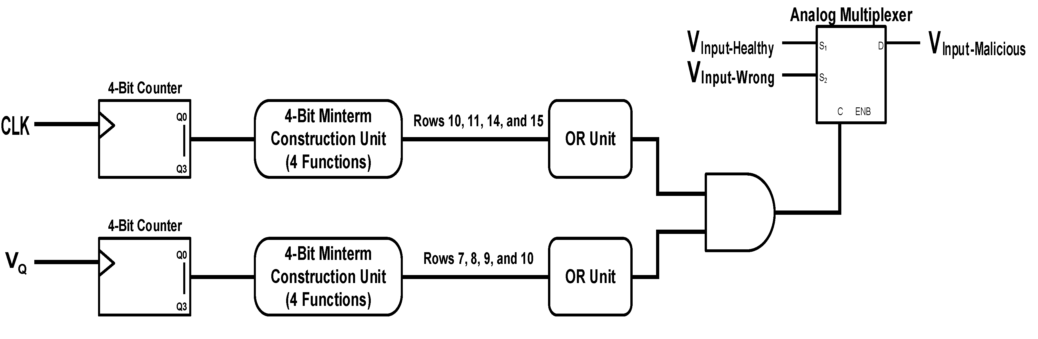
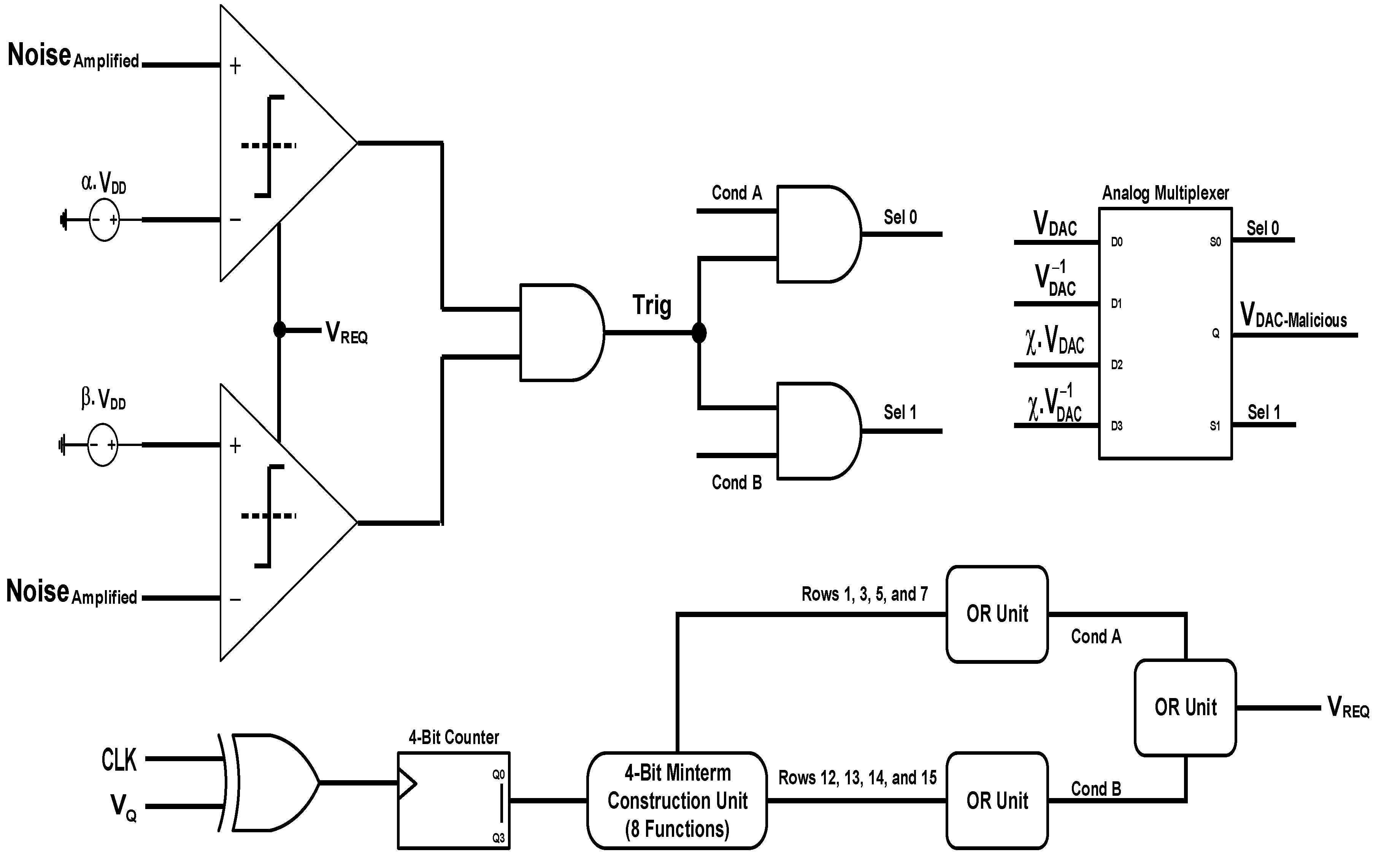
The threat model for the input signal manipulation is described as applying a wrong version of the input signal instead of the original (or healthy) version to the modulator sometimes. The wrong input signal is a version of the healthy input signal with a difference in its frequency (or period) and/or amplitude. In here, the same frequency is chosen for the wrong signal and its amplitude is specified to be one-third of the healthy signal amplitude. Therefore, when the maximum amplitude of the healthy signal is equal to
, the maximum amplitude of the wrong signal is equal to
. Applying either the healthy signal or the wrong signal is determined by an analog multiplexer. When the select signal of this multiplexer is equal to logic zero, the healthy signal is applied to the modulator; otherwise the wrong signal is applied. The select signal is made by an AND gate that has two inputs: (1) the output of the top-path circuit; and (2) the output of the bottom-path circuit. The top-path circuit can be described is this way: the system clock signal triggers a four-bit counter. The four output bits of the counter can construct up to sixteen Boolean functions based on the respective truth table. Four functions are chosen randomly (which are the 10th, 11th, 14th and 15th rows of the truth table) and built in the four-bit Minterm construction unit. The outputs of these functions are sent to an OR unit that makes the top-path circuit output equal to logic one when the output of any of the four functions becomes one. The bottom-path circuit has the same structure as the top-path circuit with the difference of having the modulator output bit as the trigger signal for the four-bit counter. Also, the chosen random functions for the four-bit Minterm construction unit are the 7th, 8th, 9th and 10th rows of the related truth table. The circuit for this attack is shown in
Figure 3. According to the figure,
is the clock signal,
is the modulator output bit,
is the healthy input signal,
is the wrong input signal, and
is the output signal of the analog multiplexer that is applied to the modulator. Meanwhile, the structure and size of the components in the Trojan circuit may be changed based on the attacker flexibilities and restrictions.
2.2. Attack 2: Noise-Triggered Output Signal Manipulation
The threat model for the output signal manipulation, triggered by noise signal is described as manipulating the DAC output signal through making it inverted, attenuated, or inverted and attenuated together sometimes. The circuit for this attack is shown in
Figure 4. The manipulation function is performed by an analog multiplexer. When the select signals of the multiplexer (
0 and
1) both are equal to logic zero, the healthy output signal (
) is transmitted. When
0 is equal to logic one while the other select signal is equal to logic zero, then the inverted version of the output signal (
) is transmitted. When
1 becomes equal to logic one and the other select signal becomes equal to logic zero, then the attenuated version of the output signal is transmitted. For attenuation,
of the signal amplitude is considered, meaning
. When both of the select signals are equal to logic one, then the inverted and attenuated version of the output signal (
) is transmitted. The select signals are produced in this way: a source of noise within the design/chip is found and amplified. The amplified noise is compared against a high threshold voltage (
) and a low threshold voltage (
) using the top and the bottom comparators. The comparators are enabled by a request signal (
). Next, the outputs of the comparators go to an AND gate in order to generate a trigger signal (
).
0 is generated by executing an AND function on the trigger signal and a condition signal, called
A. Running an AND function on the trigger signal and another condition signal, called
B produces
1. Now, let’s discuss how
,
A, and
B are generated. The system clock signal (
) and the modulator output bit (
) are dispatched to an XOR gate. The gate output signal triggers a four-bit counter. The four output bits of the counter can construct up to sixteen Boolean functions based on the respective truth table. Eight functions are chosen randomly and divided into two clusters: (Cluster A) the 1st, 3rd, 5th and 7th rows of the truth table, and (Cluster B) the 12th, 13th, 14th and 15th rows of the truth table.
A is made by sending the functions of cluster “A” to an OR unit. Similarly,
B is made through this flow. The request signal (
) is obtained by forwarding the condition signals (
A and
B) to an OR gate/unit. Meanwhile, the structure and size of the components in the Trojan circuit may be changed based on the attacker flexibilities and restrictions.
2.3. Attack 3: Controllable Manipulation of Modulator Output Bit
The threat model for controllable manipulation of the modulator output bit is described as sending the inverted version of the modulator output bit (or the bit stream) to the digital filter block at any time by controlling the supply voltage of a maliciously sized TFET-based static random-access memory (SRAM) cell [
27,
28,
29] locally or globally. The nodes of the TFET-based SRAM cell can be described as:
and
are the bit lines,
and
are the storing nodes for the data bit,
1 and
0 are the control signals for storing logic one and logic zero respectively,
and
are the supply voltage and ground respectively. This SRAM cell is sized maliciously in order to make the write operation possible only when the supply voltage is set in
to
range. In other words, if the supply voltage is set to a value outside this range, such as
, neither logic zero nor logic one can be stored in this cell. In fact, this is an escape path for the attack since when most (if not all) of the circuit/system elements operate perfectly at the supply voltage of
, the Hardware Trojan is dormant. On the other hand, if it is set to a value such as
, all the circuit/system elements along with the Hardware Trojan are active. There are a number of possibilities for performing the malicious cell sizing: (1) physically inside the untrusted foundry; (2) applying malicious modifications within the algorithms utilized for sizing the design cells; and (3) designing a few malicious cells and inserting them inside the chip during application specific integrated circuit (ASIC) design flow [
30,
31,
32,
33,
34]. Adjusting the supply voltage can be done internally through predefined circuit/system conditions or externally by a malicious person. Changing the supply voltage can be done locally only for this SRAM cell or globally for the whole chip. It is assumed that the malicious SRAM cell is asleep when the supply voltage is out of its working range due to predefined manipulation of the Gated Supply Voltage mechanism [
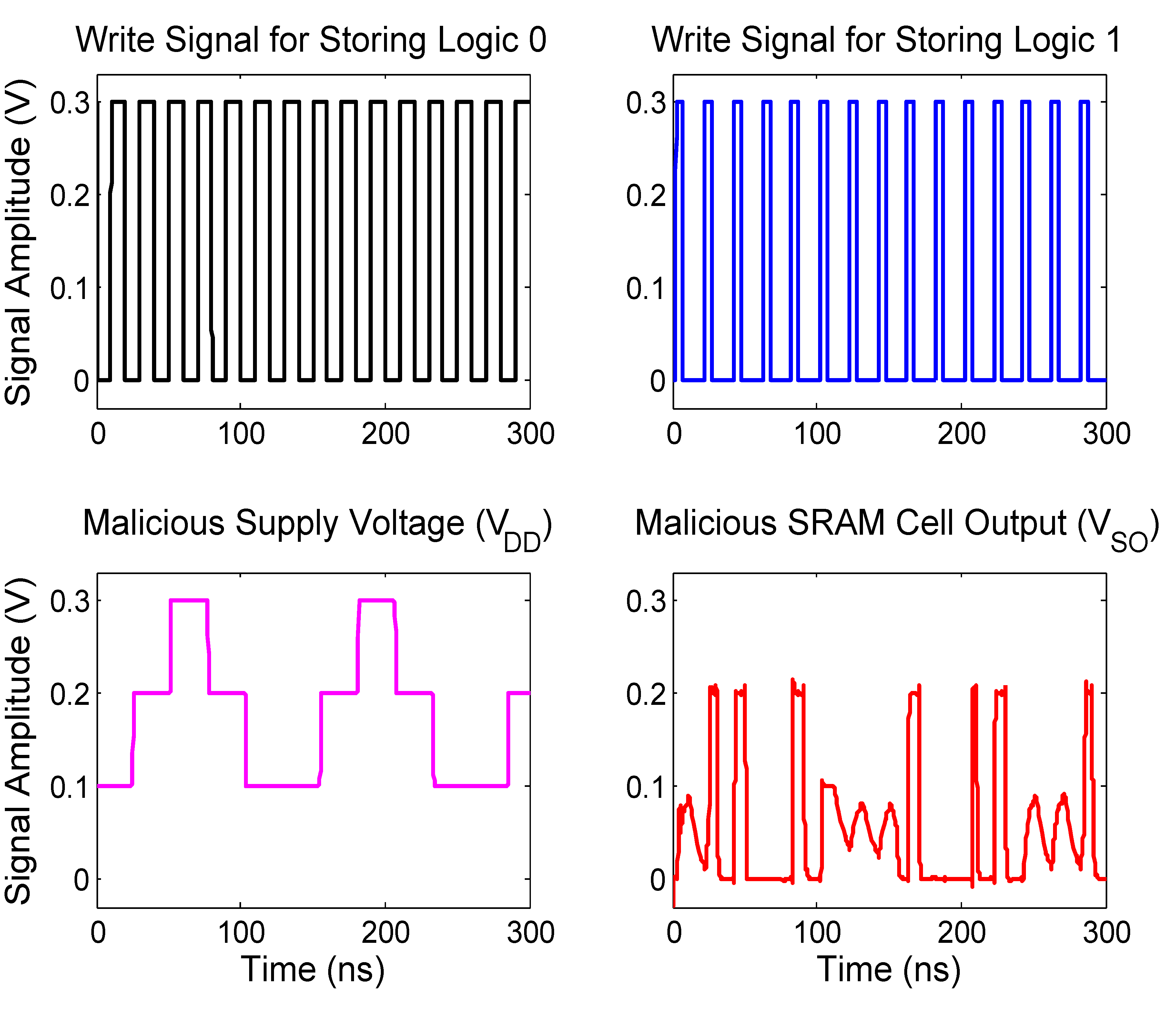
35], which is an architectural approach for reduction of leakage power consumption. In this way, the malicious SRAM cell does not contribute to the chip functionality and no functionality failure occurs before activation of the Hardware Trojan (which means when the supply voltage is at its typical value). In this work, local malicious variations of the supply voltage for the SRAM cell is considered. The malicious TFET-based SRAM cell is sized through parametric simulation and analysis, and the achieved values are: the channel length of all transistors is set to 20 nm, the width of pull-up transistors is set to 20 nm, the width of pull-down transistors is set to 45 nm, the width of access transistors for writing logic zero is set to 45 nm, and the width of access transistors for writing logic one is set to 35 nm.
Figure 5 displays a simulation of this circuit with these specifications:
is set to
and the other bit line is set to ground (or logic zero),
1 is a pulse signal with the delay of 2.5 ns, the width of 5 ns, the period of 20 ns, and the amplitude of
,
0 is a pulse signal with the width of 10 ns, the period of 20 ns, and the amplitude of
, and the supply voltage is a piecewise linear waveform with three states. Each state takes 25 ns, and the amplitude of these states are 0.1 V, 0.2 V, and 0.3 V. The duration time for the transient simulation and analysis is set to 300 ns. It can be understood from this figure that the correct write operations (either for logic zero or logic one) on the storing node (
) occurs when the supply voltage is equal to 0.2 V. Just as a clarification, the
notation of the malicious supply voltage is different than the maximum amplitude of the other circuit signals. Now, let’s get back to the controllable Hardware Trojan circuit for manipulation of the modulator output bit (shown in
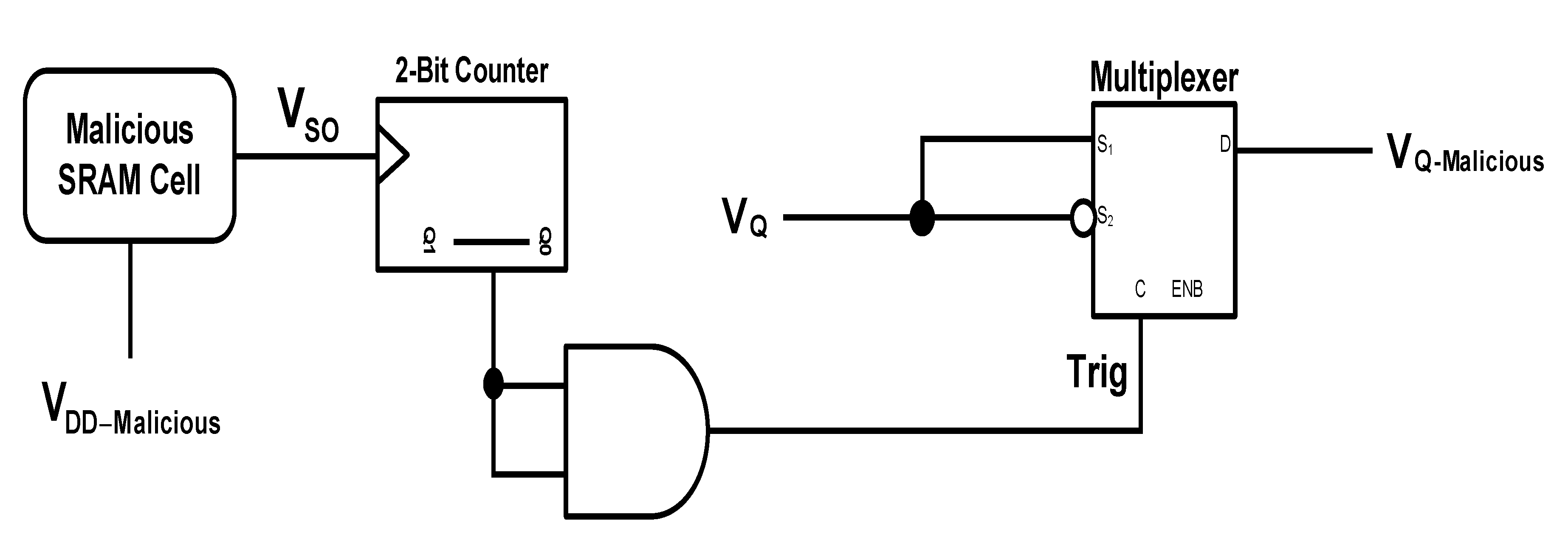
Figure 6). The supply voltage under manipulation (or the malicious supply voltage) is connected to the malicious SRAM cell. The voltage signal at the cell storing node triggers a two-bit counter. The counter output bits are sent to an AND unit. The result signal (
) is the select signal of a multiplexer that dispatches the inverted version of the modulator output bit to the digital filter block whenever it is equal to logic one. In order to “model” this attack for the
modulator, the supply voltage of the malicious SRAM cell is manipulated locally throughout the circuit operation. Meanwhile, the structure and size of the components in the Trojan circuit may be changed based on the attacker flexibilities and restrictions.
2.4. Attack 4: Capacitance-Triggered Output Signal Manipulation
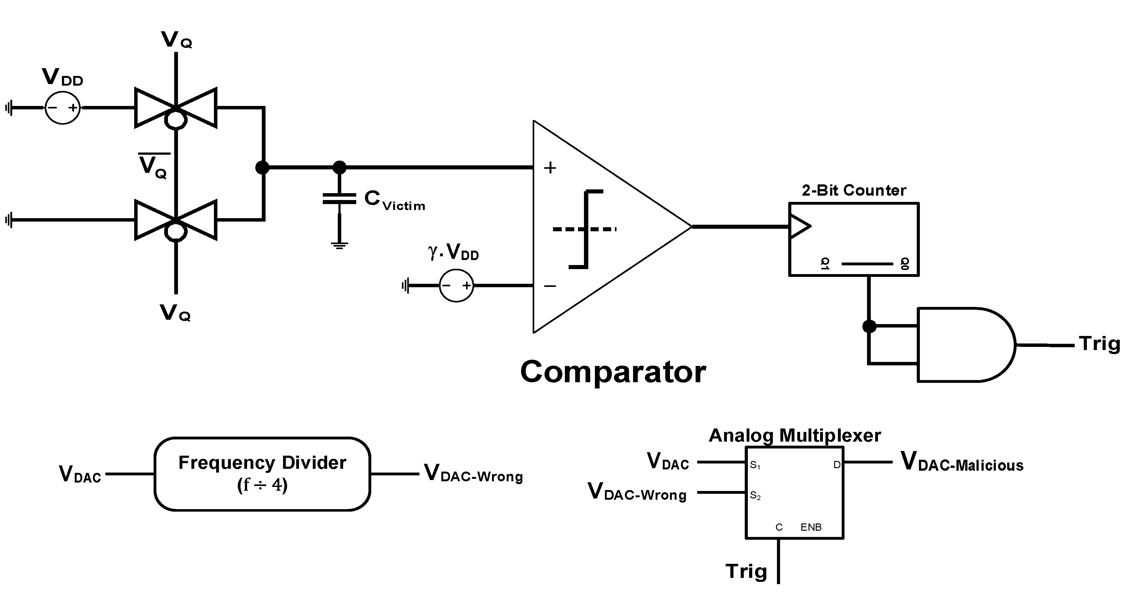
The threat model for the output signal manipulation, triggered by a victim capacitance is described as manipulating the DAC output signal through transmitting a frequency-divided version of it (instead of the original version) sometimes. The victim capacitance can be realized at the fabrication-level by targeting an interconnect capacitance (which is the capacitance among the metal layer connections in different regions of the chip) or a transistor-associated capacitance (such as the quantum capacitance of the channel). The circuit for this attack is shown in
Figure 7. The flow of this circuit can be described in this way: the victim capacitance is charged or discharged through connection of its positive terminal to the supply voltage or the ground respectively. The negative terminal of the victim capacitance is always connected to the ground. The decision on charging or discharging the capacitance is made by the modulator output bit. Then, the signal at the positive terminal of the capacitance is compared against a threshold voltage (
). If the amount of charge stored on the victim capacitance exceeds the threshold voltage, the comparator delivers logic one. The comparator output signal triggers a two-bit counter. The counter output bits go to an AND gate that delivers
signal. Whenever this signal becomes equal to logic one, the DAC output signal with its frequency divided by four is transferred by an analog multiplexer. The frequency-divided version of the DAC output signal is provided by a frequency divider. Meanwhile, the structure and size of the components in the Trojan circuit may be changed based on the attacker flexibilities and restrictions.
2.5. Defense: Output Signal Filtering
In signal processing, a filter is a computational process that eliminates some unwanted components or features from a signal. In other words, the important parts of information are extracted, while random and undesired features, such as noise, are eliminated. The filtering process can be performed on the time-domain or frequency-domain. The functionality of a filter can be classified as: (a) signal separation; and (b) signal restoration. Signal separation is used when a signal has been infected with noise or any other type of interfering signal. Signal restoration is used when a signal has been distorted. Curve-fitting is the process of constructing a mathematical function/model that has the best fit to a signal [
36,
37,
38,
39]. The mathematical model can act as a filtering process through interpolation operation (which means finding an exact fit) or smoothing operation (which means finding an approximate fit). In a good fit, the main behavior of signal along with the important signal patterns are well discovered and the unpleasant elements are left out. In fact, the signal to noise ratio is increased and the difference between the mathematical model (or specifically the predicted signal by the model) and the actual signal is minimized.
In order to measure the goodness of the model fit, a statistical parameter called R-squared () or the coefficient of determination is introduced. This parameter is defined as the proportion of the variance in the dependent variable that is predictable from the independent variable(s). The main element in calculating the R-squared parameter is the error data (or the Residuals) that is defined as: . The residual plot can reveal hidden patterns visually and more effectively. Meanwhile, a negative R-squared value (or a reverse R-squared value) is obtained when the mathematical model does not follow the signal behavior, which indicates a very bad data fitting. Although a large magnitude for the R-squared parameter demonstrates a higher level of relationship between the actual signal and the predicted signal, regardless of its sign.
In this work, the curve-fitting models are utilized within the bureau of intelligence and investigation (or the CIU) in order to filter the infected DAC output signal and eliminate the malicious intentional noise/features, introduced by a Hardware Trojan. In this context, the formula for the residual parameter is modified as follows: . The reference signal is a trustworthy DAC output signal. The filtered signal is the outcome of running a filter on the DAC output signal under security checking. The modified R-squared parameter is calculated accordingly. Some curve-fitting models need the reference signal for carrying out the filtering process, while others do not. The employed models for filtering the DAC output signal are: (1) simple linear regression; (2) generalized linear regression; (3) moving average; (4) robust regression with the least absolute residual (LAR) computing method; (5) robust regression with the bi-squared computing method; (6) median filtering; (7) Savitzky-Golay filtering; (8) autoregressive-moving-average model with exogenous inputs (ARMAX); and (9) region of interest (ROI) filtering. For applying each of these filters, all the signals are prepared (in terms of scaling, offset elimination, and so forth) accordingly.
In this work, the selected configurations for the models are: (a) the simple linear regression has the degree of one; (b) the distribution model of the generalized linear regression is Gamma and its link function is reciprocal; (c) the window size for moving average is equal to 15,000; (d) the selected frame-length for the Savitzky–Golay filter is equal to 10,001, and its order is equal to one; (e) the order of all the elements of the ARMAX model is equal to 10; and (f) the positive and the negative peaks of the DAC output signal for any waveform is strictly filtered based on the convention of having no spikes and noticeable variations in those regions in the ROI filtering. Meanwhile, it is assumed that there is no time-misalignment between the input signal applied to the filter and its output signal.
3. Results and Discussion
In this section, the functionality of the first-order one-bit
modulator is evaluated in six different structures: (A) “Healthy ADC”, in which no malicious change is carried out on the modulator circuit; (B) “ADC Under Attack 1”, in which the input signal to the modulator is manipulated; (C) “ADC Under Attack 2”, in which the modulator output signal is manipulated according to a noise-triggered mechanism; (D) “ADC Under Attack 3”, in which the modulator output bit is manipulated based on controlling the supply voltage; (E) “ADC Under Attack 4”, in which the modulator output signal is manipulated according to a capacitance-triggered mechanism; and (F) “Security Enhanced ADC”, in which the central intelligence unit is added to the ADC architecture as a countermeasure against possible threats. All these circuit structures are implemented using 20 nm AlGaSb/InAs tunnel field effect transistor technology (provided in the Universal TFET model 1.6.8 [
22]). In these implementations, all the circuit elements are sized through parametric simulation and analysis. Also, the main goal was only “functional correctness” during the design and implementation of these circuits due to the chosen type of payload for the Hardware Trojans.
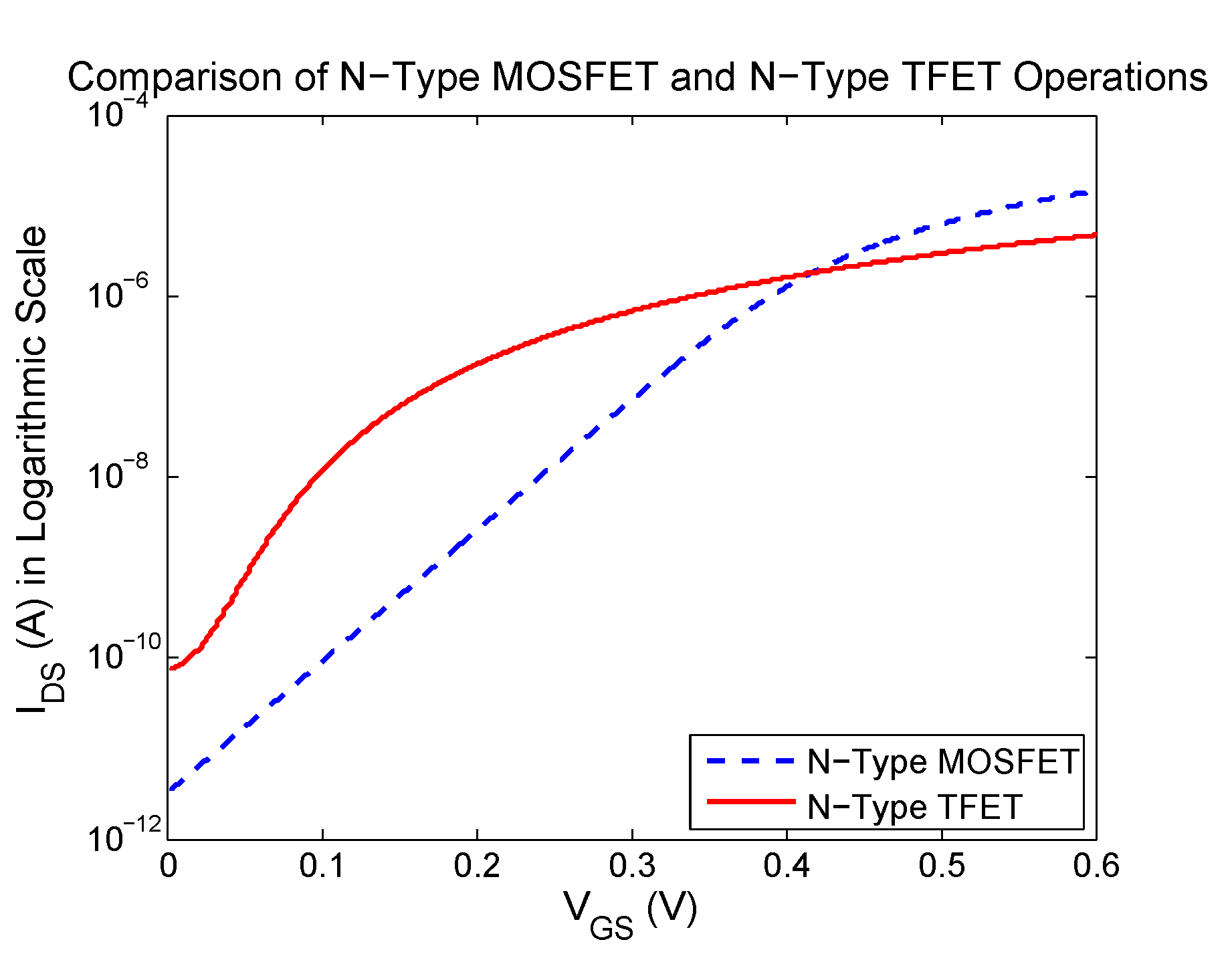
TFET provides steeper sub-threshold slope, smaller than 60 mV/dec [
40], and is described as a gated p-i-n (which is the hole-dominant region, the intrinsic or pure region, and the electron-dominant region) diode that has asymmetrical doping structure and operates under reverse-bias condition. The steeper sub-threshold slope of the TFET device helps further downscale the supply voltage and reduce the leakage currents substantially, which makes it an excellent candidate to achieve low energy consumption for the smart electronic devices. The comparison between the drain-source current (
) versus gate-source voltage (
) curves of the n-type MOSFET and the n-type TFET is shown in
Figure 8. For simulating this plot, both devices have the same width and length of 20 nm and are connected to the supply voltage of 0.6 V. As it can be seen from the figure, the TFET device turns on and goes to its saturation region at a smaller value of the gate-source voltage compared to the MOSFET device. Thus, the TFET technology is favorable for low voltage design.
The Cadence Spectre Circuit Simulator is used for simulation and analysis of the implemented circuit structures. The duration time for the transient analysis is set to 10 s, the clock signal has a pulse width of 1 ns, a period of 2 ns, and a delay of 10 ns, the reset signal has a pulse width of 5 ns and a period that is out of the scope of transient analysis, and the supply voltage is set to 0.3 V (in all of the components, except the operational amplifier in which it is set to 1.8 V) for all of the simulations run. In order to carry out a complete functional analysis of these circuit structures, three types of waveforms are applied to the modulator input terminal that are sinusoidal, triangle, and sawtooth. The period of the input signal for all these waveforms is set to 5 s. Meanwhile, the maximum amplitude of all the aforementioned signals is set to 0.3 V. Extracted from the simulation results for the sinusoidal input signal, the root mean square (RMS) power consumption of the main supply voltage is equal to 121.9 nW and the average power consumption of the main supply voltage is equal to 87.12 nW. Due to the noticeable power consumption of the op-amp-based modulator components, the impact of Hardware Trojans on the modulator power consumption is negligible. The delay overhead (on the modulator circuit) caused by the first attack is 0.31%, the second attack is 3.96%, the third attack is 13.17%, and the fourth attack is 6.93%. The area footprint (on the modulator circuit) caused by the first attack is 1.63%, the second attack is 3.95%, the third attack is 0.21%, and the fourth attack is 4.19%. Again, these overheads are not significant when the share of the modulator within the whole ADC architecture (and the SoC design) is taken into account.
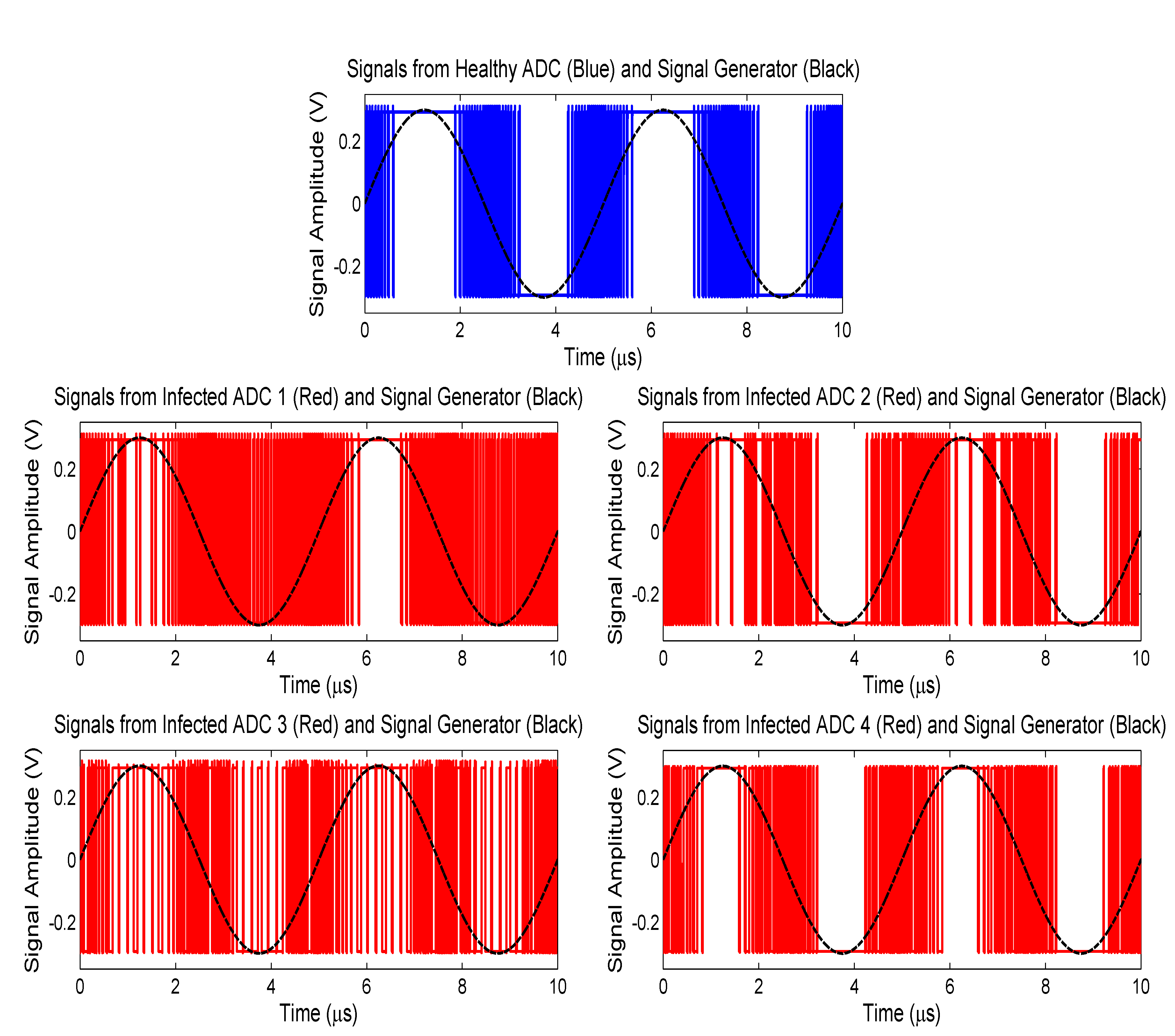
The functional simulation of the modulator circuit for the structures “A” to “E” is shown in
Figure 9. According to the figure, all the Hardware Trojans damage the modulator output signal. The first attack ruins the signal negative peaks very aggressively. The malicious changes caused by this attack on the first positive peak is at a high-level, while it is mild for the second positive peak. The second attack brings a large number of spikes in the signal positive peaks, while its alterations in the negative peaks are small. The third attack makes distributed large variations in both positive and negative peaks. The fourth attack forms considerable fluctuations in the signal positive peaks, while its impact is small on the negative peaks. The effects of all these attacks can also be observed more or less in the regions of signal transitions. All these malicious traces can shape meaningful and catastrophic consequences in both analog and digital domains.
Now, the performance of the discussed filters in eliminating the payloads of Trojans are analyzed based on their delivering modified R-squared values. Let’s take a look at
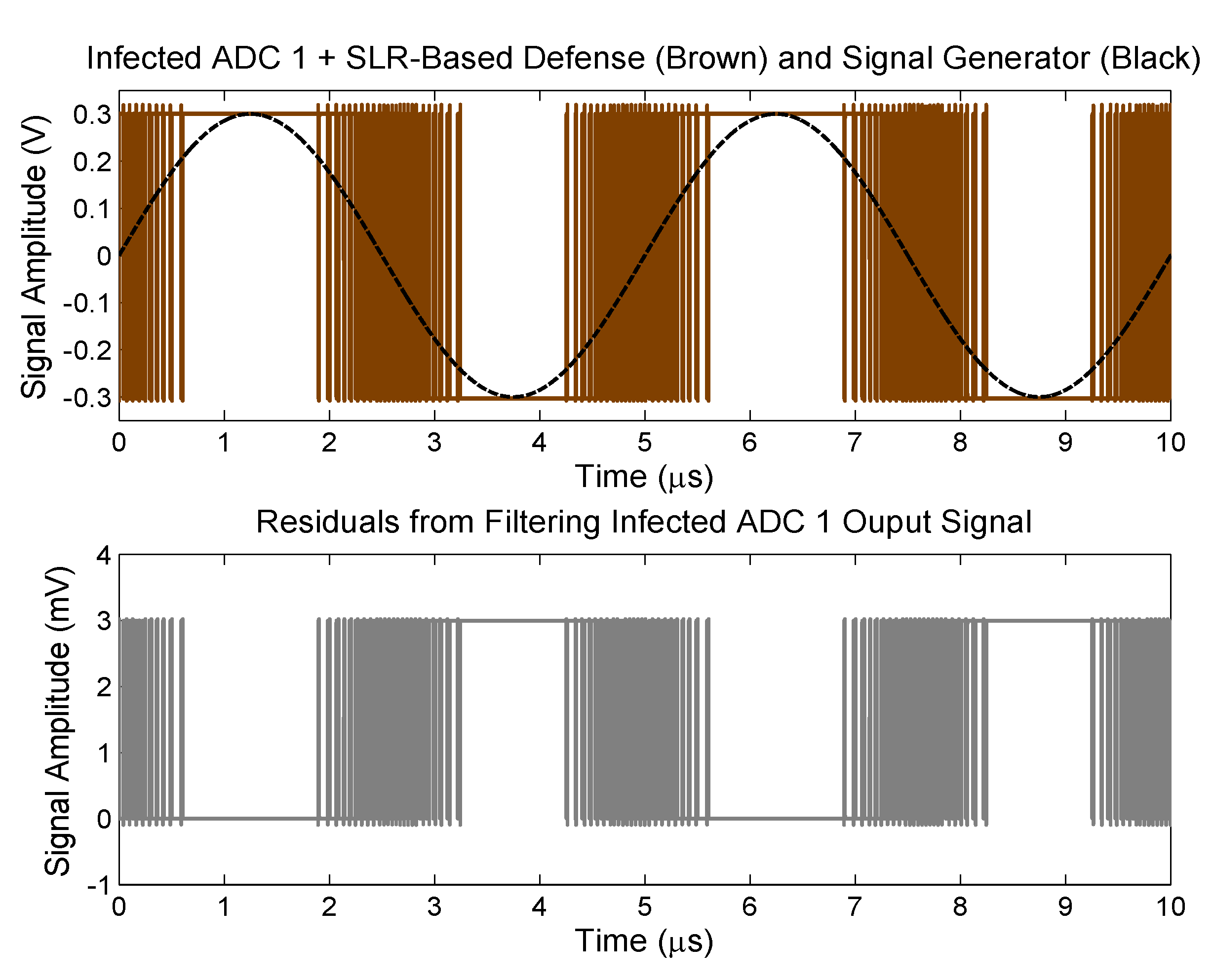
Figure 10 that shows an example of the filtered modulator output signal by the simple linear regression method (in the top plot) and the residuals from this filtering process (in the bottom plot). According to the top plot, the simple linear regression method demonstrates effectiveness in removing the malicious intentional spikes, especially in the positive and the negative signal peaks. The residual plot and its order of magnitude displays the quality of filtering process even further.
Table 1,
Table 2 and
Table 3 present a complete performance analysis of the filters in confronting the four attacks, when the three types of waveforms are applied to the modulator. According to the results, the best filter in facing the Trojans is the robust regression using the least absolute residual computing method, and the worst one is the Savitzky-Golay filtering (based on the absolute value of the modified R-squared values). It implies that a linear filter using an effective error minimization method is a good candidate for defeating the attacks. In order to achieve higher performance, a number of these filtering techniques may be combined together (known as hybrid filtering). Also, a threshold value can be considered for the R-squared parameter according to which a filtered signal is rejected if its
value is below the threshold (which means the filtered signal is not close enough to the reference signal). The threshold value of 0.9 is a worthy option for signal rejection and user notification. Meanwhile, the second threat model exhibits the strongest attack according to the simuation results.
In order to assess the defense capabilities of the filters under the effects of process variations, the first defense analysis is conducted in two more experiments according to which the threshold voltage of the tunnel field effect transistors are changed to 20% higher and 20% lower than its typical value. The results of these two experiments are shown in
Table 4 and
Table 5 respectively. The robust regression using the least absolute residual computing method is immune in front of the effects of process variations, while the other filters show diverse behavior in attenuating/eliminating the payload of the Trojans.


