
Modeling and Design of a New Flexible Graphene-on-Silicon Schottky Junction Solar Cell


Abstract
:1. Introduction
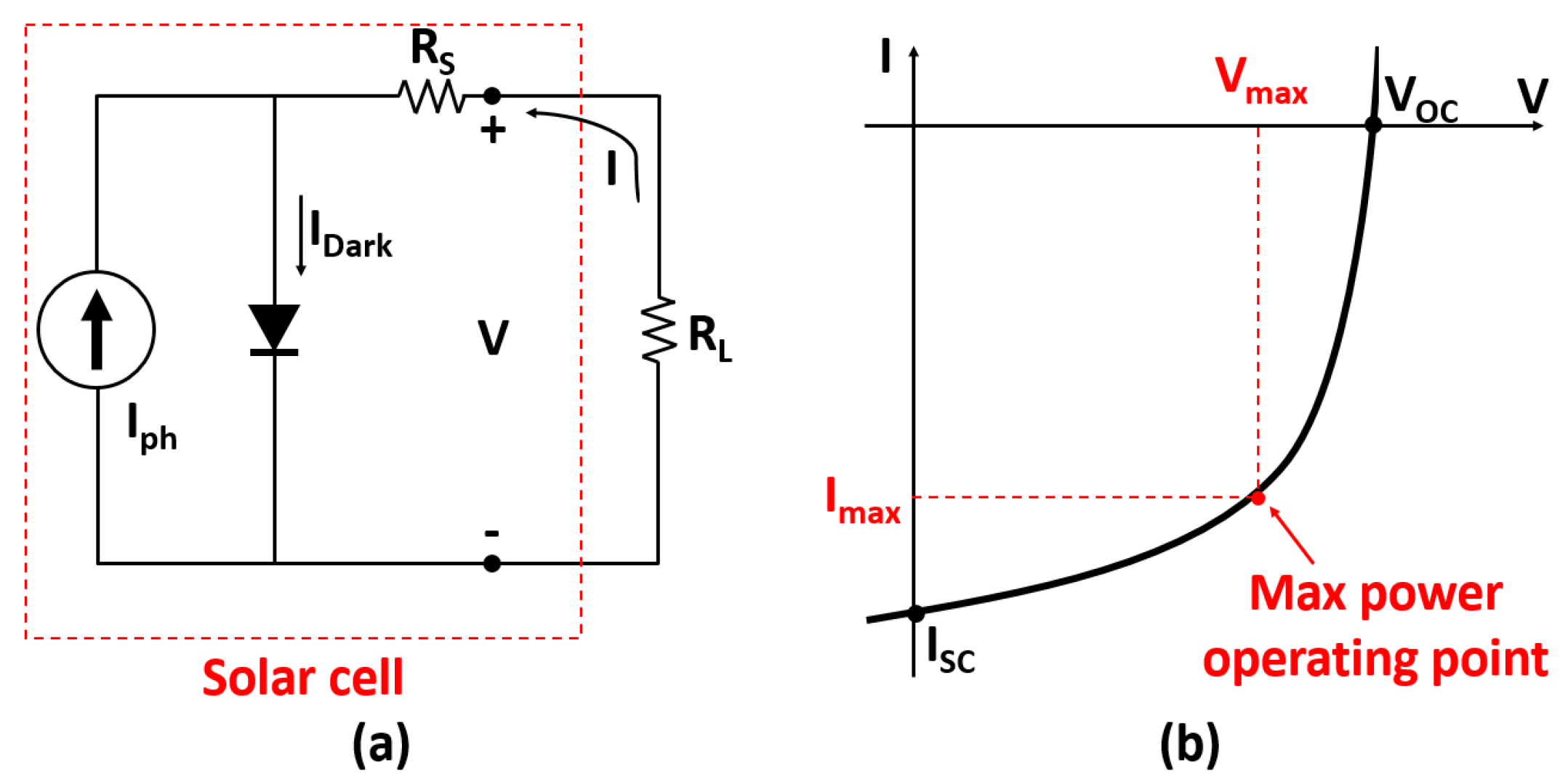
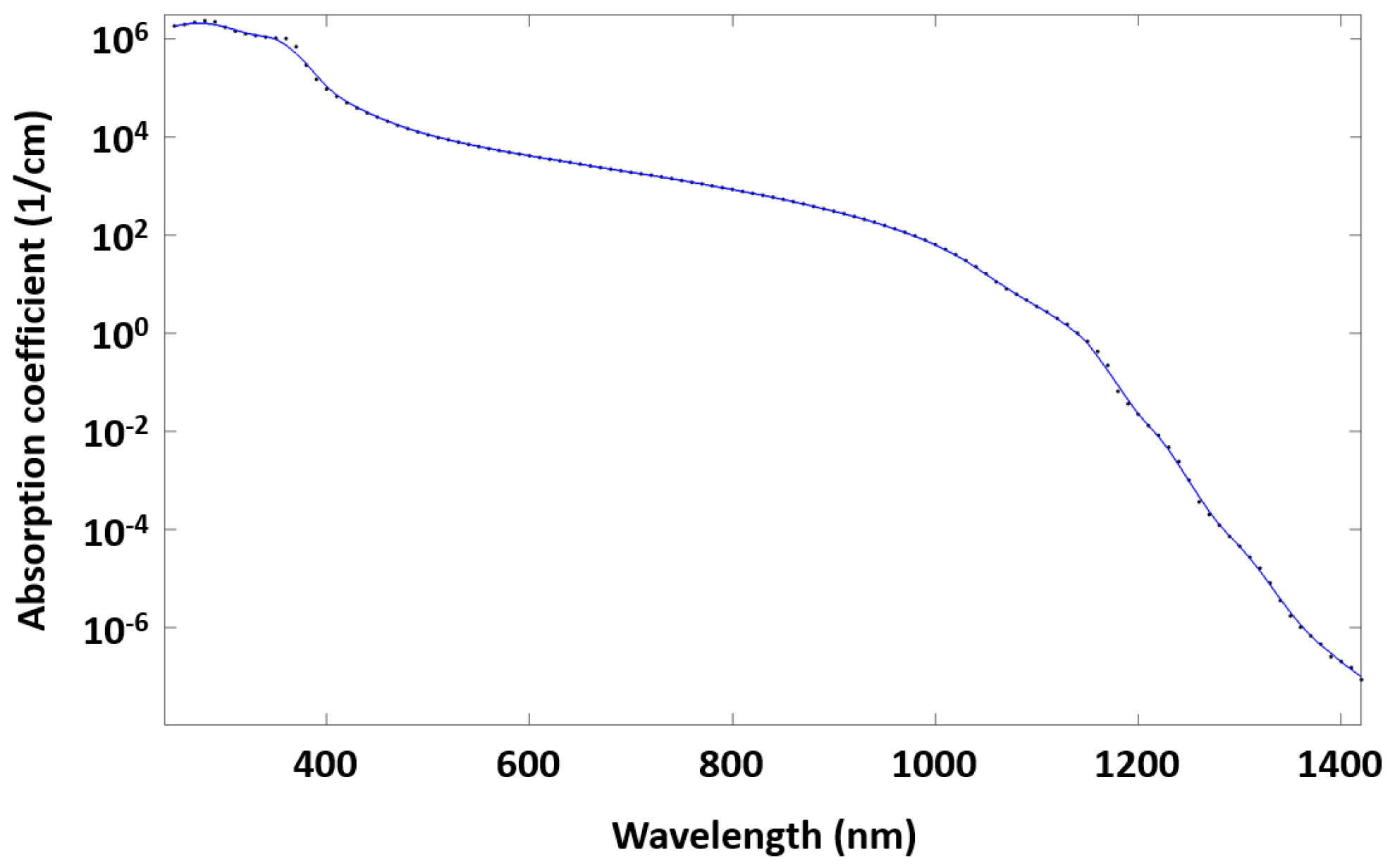
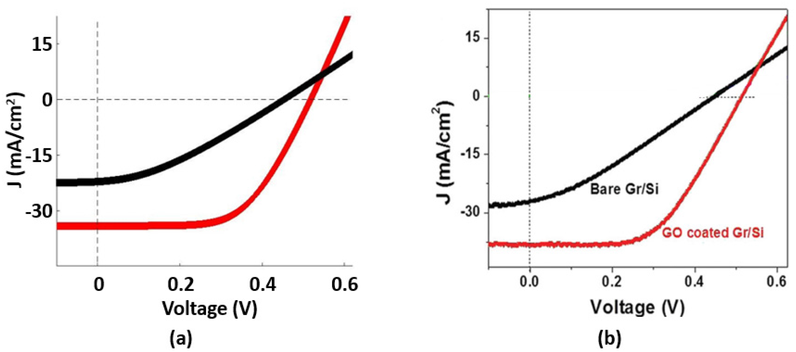
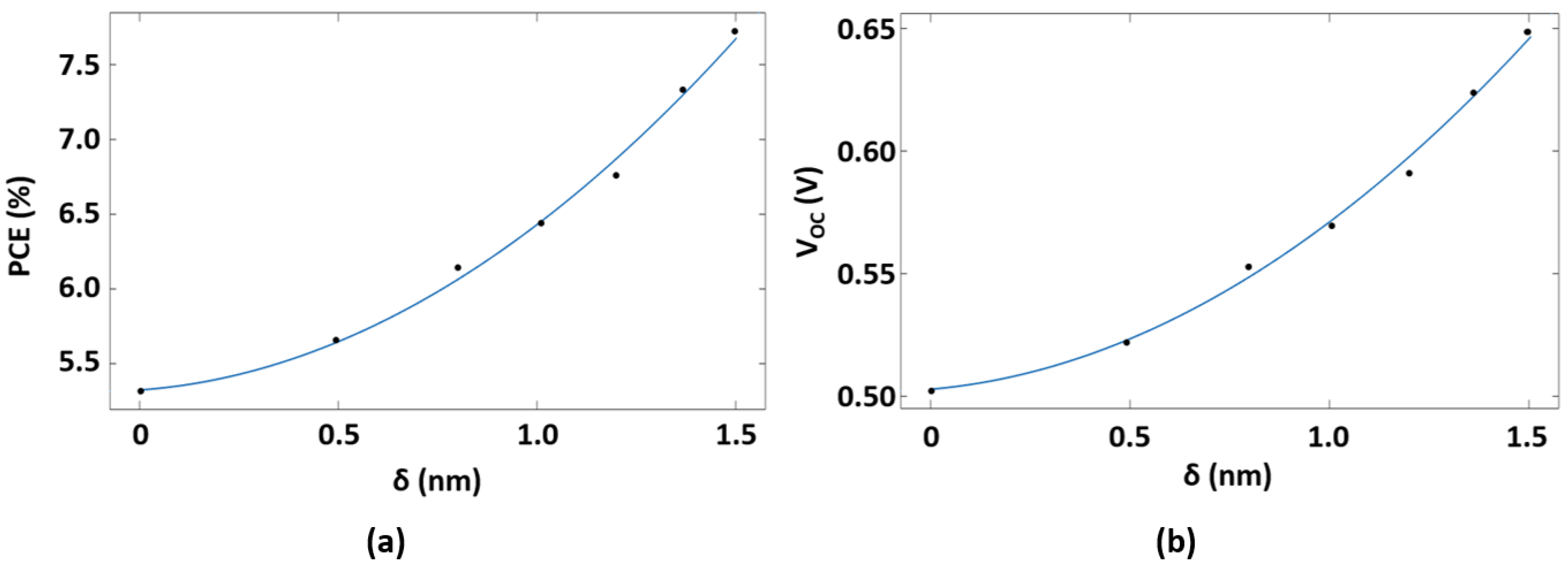
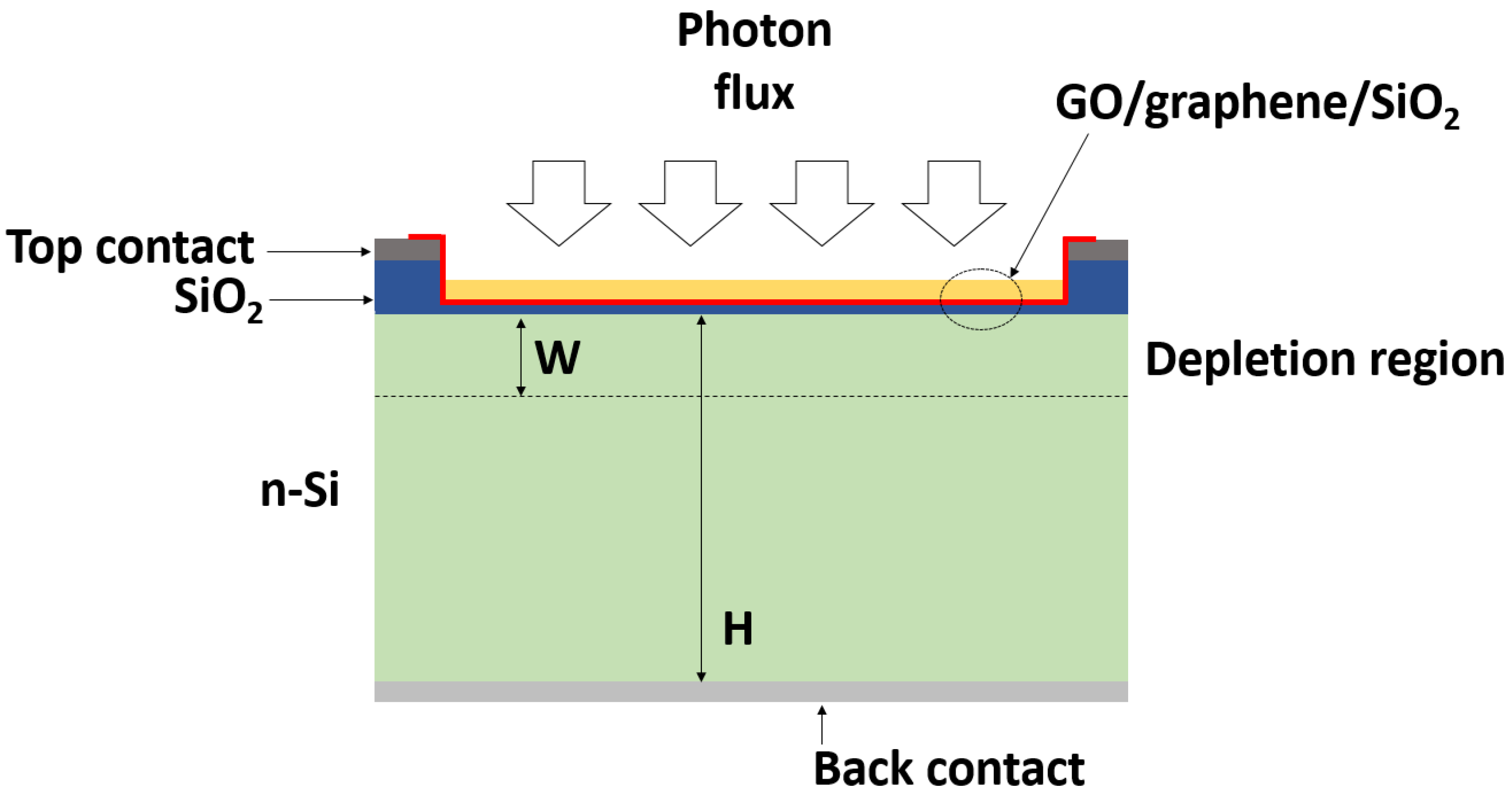
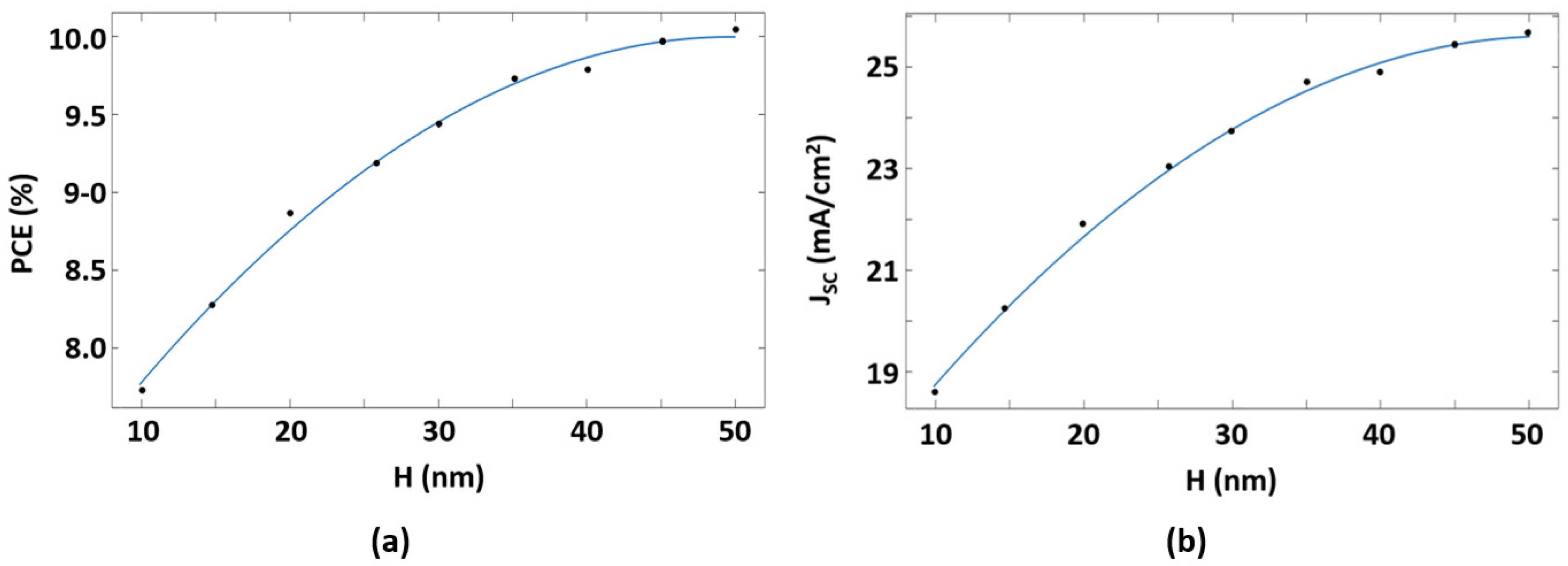
2. Solar Cell Model
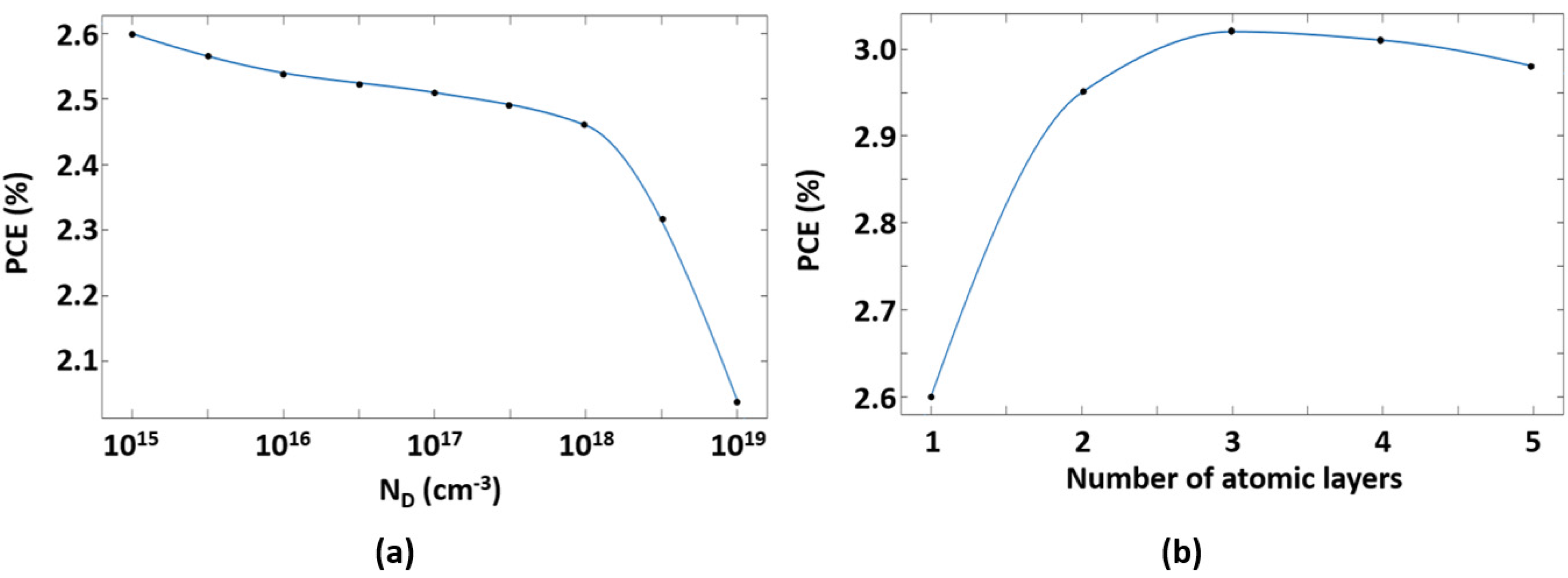
3. Solar Cell Design
4. Conclusions
Author Contributions
Conflicts of Interest
References
- Warner, J.H.; Schaffel, F.; Rummeli, M.; Bachmatiuk, A. Graphene: Fundamentals and Emergent Applications; Elsevier: Waltham, MA, USA, 2013. [Google Scholar]
- Choi, W.; Lee, J. Graphene: Synthesis and Applications; CRC Press: Boca Raton, FL, USA, 2016. [Google Scholar]
- Novoselov, K.S.; Fal’ko, V.I.; Colombo, L.; Gellert, P.R.; Schwab, M.G.; Kim, K. A roadmap for graphene. Nature 2012, 490, 192–200. [Google Scholar] [CrossRef] [PubMed]
- Bonaccorso, F.; Sun, Z.; Hasan, T.; Ferrari, A.C. Graphene photonics and optoelectronics. Nat. Photonics 2010, 4, 611–622. [Google Scholar] [CrossRef]
- Liu, M.; Yin, X.; Ulin-Avila, E.; Geng, B.; Zentgraf, T.; Ju, L. A graphene-based broadband optical modulator. Nature 2011, 474, 64–67. [Google Scholar] [CrossRef] [PubMed]
- Xia, F.; Mueller, T.; Lin, Y.; Valdes-Garcia, A.; Avouris, P. Ultrafast graphene photodetector. Nat. Nanotechnol. 2009, 4, 839–843. [Google Scholar] [CrossRef] [PubMed]
- Bao, Q.; Zhang, H.; Wang, Y.; Ni, Z.; Yan, Y.; Shen, Z.X.; Loh, K.P.; Tang, D.Y. Atomic-Layer Graphene as a Saturable Absorber for Ultrafast Pulsed Lasers. Adv. Funct. Mater. 2009, 19, 3077–3083. [Google Scholar] [CrossRef]
- Yahiaoui, R.; Guillet, J.P.; de Miollis, F.; Mounaix, P. Ultra-flexible multiband terahertz metamaterial absorber for conformal geometry applications. Opt. Lett. 2013, 38, 4988–4990. [Google Scholar] [CrossRef] [PubMed]
- Yahiaoui, R.; Hanai, K.; Takano, K.; Nishida, T.; Miyamaru, F.; Nakajima, M.; Hangyo, M. Trapping waves with terahertz metamaterial absorber based on isotropic Mie resonators. Opt. Lett. 2013, 40, 3197–3200. [Google Scholar] [CrossRef] [PubMed]
- Bao, Q.; Zhang, H.; Wang, B.; Ni, Z.; Lim, C.H.Y.X.; Wang, Y.; Tang, D.Y.; Loh, K.P. Broadband graphene polarizer. Nat. Photonol. 2011, 5, 411–415. [Google Scholar] [CrossRef]
- Conteduca, D.; Dell’Olio, F.; Ciminelli, C.; Armenise, M.N. Resonant Graphene-Based Tunable Optical Delay Line. IEEE Photonics J. 2015, 7, 7802409. [Google Scholar] [CrossRef]
- Tatoli, T.; Conteduca, D.; Dell’Olio, F.; Ciminelli, C.; Armenise, M.N. Graphene-based fine-tunable optical delay line for optical beamforming in phased-array antennas. Appl. Opt. 2016, 55, 4342–4349. [Google Scholar] [CrossRef] [PubMed]
- Capmany, J.; Domenech, D.; Muñoz, P. Silicon graphene waveguide tunable broadband microwave photonics phase shifter. Opt. Express 2014, 22, 8094–8100. [Google Scholar] [CrossRef] [PubMed]
- Yin, Z.; Zhu, J.; He, Q.; Cao, X.; Tan, C.; Chen, H.; Yan, Q.; Zhang, H. Graphene-Based Materials for Solar Cell Applications. Adv. Energy Mater. 2014, 4, 1300574. [Google Scholar] [CrossRef]
- Loh, K.P.; Tong, S.W.; Wu, J. Graphene and Graphene-like Molecules: Prospects in Solar Cells. J. Am. Chem. Soc. 2016, 138, 1095–1102. [Google Scholar] [CrossRef] [PubMed]
- You, P.; Liu, Z.; Tai, Q.; Liu, S.; Yan, F. Efficient Semitransparent Perovskite Solar Cells with Graphene Electrodes. Adv. Mater. 2015, 27, 3632–3638. [Google Scholar] [CrossRef] [PubMed]
- Park, H.; Chang, S.; Zhou, X.; Kong, J.; Palacios, T.; Gradečak, S. Flexible Graphene Electrode-Based Organic Photovoltaics with Record-High Efficiency. Nano Lett. 2014, 14, 5148–5154. [Google Scholar] [CrossRef] [PubMed]
- Tong, S.W.; Wang, Y.; Zheng, Y.; Ng, M.; Loh, K.P. Graphene Intermediate Layer in Tandem Organic Photovoltaic Cells. Adv. Funct. Mater. 2011, 21, 4430–4435. [Google Scholar] [CrossRef]
- Ameen, S.; Shaheer Akhtar, M.; Seo, H.-K.; Nazeeruddin, M.K.; Shin, H.S. An Insight into Atmospheric Plasma Jet Modified ZnO Quantum Dots Thin Film for Flexible Perovskite Solar Cell: Optoelectronic Transient and Charge Trapping Studies. J. Phys. Chem. C 2015, 119, 10379–10390. [Google Scholar] [CrossRef]
- Wang, J.T.; Ball, J.M.; Barea, E.M.; Abate, A.; Alexander-Webber, J.A.; Huang, J.; Saliba, M.; Mora-Sero, I.; Bisquert, J.; Snaith, H.J.; et al. Low-Temperature Processed Electron Collection Layers of Graphene/TiO2 Nanocomposites in Thin Film Perovskite Solar Cells. Nano Lett. 2014, 14, 724–730. [Google Scholar] [CrossRef] [PubMed]
- Gao, P.; Ding, K.; Wang, Y.; Ruan, K.; Diao, S.; Zhang, Q.; Sun, B.; Jie, J. Crystalline Si/Graphene Quantum Dots Heterojunction Solar Cells. J. Phys. Chem. C 2014, 118, 5164–5171. [Google Scholar] [CrossRef]
- Li, X.; Zhu, H.; Wang, K.; Cao, A.; Wei, J.; Li, C.; Jia, Y.; Li, Z.; Li, X.; Wu, D. Graphene-On-Silicon Schottky Junction Solar Cells. Adv. Mater. 2010, 22, 2743–2748. [Google Scholar] [CrossRef] [PubMed]
- Song, Y.; Li, Y.; Mackin, C.; Zhang, X.; Fang, W.; Palacios, T.; Zhu, H.; Kong, J. Role of Interfacial Oxide in High-Efficiency Graphene—Silicon Schottky Barrier Solar Cells. Nano Lett. 2015, 15, 2104–2110. [Google Scholar] [CrossRef] [PubMed]
- Li, X.; Chen, W.; Zhang, S.; Wu, Z.; Wang, P.; Xu, Z.; Chen, H.; Yin, W.; Zhong, H.; Lin, S. 18.5% efficient graphene/GaAs van der Waals heterostructure solar cell. Nano Energy 2015, 16, 310–319. [Google Scholar] [CrossRef]
- Jiao, T.; Wei, D.; Liu, J.; Sun, W.; Jia, S.; Zhang, W.; Feng, Y.; Shia, H.; Dua, C. Flexible solar cells based on graphene-ultrathin silicon Schottky junction. RSC Adv. 2015, 5, 73202–73206. [Google Scholar] [CrossRef]
- Ruan, K.; Ding, K.; Wang, Y.; Diao, S.; Shao, Z.; Zhang, X.; Jie, J. Flexible graphene/silicon heterojunction solar cells. J. Mater. Chem. A 2015, 3, 14370–14377. [Google Scholar] [CrossRef]
- Pagliaro, M.; Palmisano, G.; Ciriminna, R. Flexible Solar Cells; Wiley VCH: Weinheim, Germany, 2008. [Google Scholar]
- Lin, Q.; Huang, H.; Jing, Y.; Fu, H.; Chang, P.; Li, D.; Yao, Y.; Fan, Z. Flexible photovoltaic technologies. J. Mater. Chem. C 2014, 2, 1233–1247. [Google Scholar] [CrossRef]
- Yin, X.; Chen, P.; Que, M.; Xing, Y.; Que, W.; Niu, C.; Shao, J. Highly Efficient Flexible Perovskite Solar Cells Using Solution-Derived NiOx Hole Contacts. ACS Nano 2016, 10, 3630–3636. [Google Scholar] [CrossRef] [PubMed]
- Berhe, T.A.; Su, W.N.; Chen, C.H.; Pan, C.-J.; Cheng, J.-H.; Chen, H.-M.; Tsai, M.-C.; Chen, L.Y.; Dubale, A.A.; Hwang, B.J. Organometal halide perovskite solar cells: Degradation and stability. Energy Environ. Sci. 2016, 9, 323–356. [Google Scholar] [CrossRef]
- Yavuz, S.; Kuru, C.; Choi, D.; Kargar, A.; Jina, S.; Bandaru, P.R. Graphene oxide as a p-dopant and an anti-reflection coating layer, in graphene/silicon solar cells. Nanoscale 2016, 8, 6473–6478. [Google Scholar] [CrossRef] [PubMed]
- Morita, M.; Ohmi, T.; Hasegawa, E.; Kawakami, M.; Ohwada, M. Growth of native oxide on a silicon surface. J. Appl. Phys. 1990, 68, 1272–1281. [Google Scholar] [CrossRef]
- Hovel, H.J. Solar Cells. Semicond. Semimet. 1975, 11, 112–148. [Google Scholar]
- Sze, S.M. Physics of Semiconductor Devices; Wiley: New York, NY, USA, 1969. [Google Scholar]
- Green, M.A.; Keevers, M.J. Optical properties of intrinsic silicon at 300 K. Prog. Photovolt. Res. Appl. 1995, 3, 189–192. [Google Scholar] [CrossRef]
- Fossum, J.G. Computer-aided numerical analysis of silicon solar cells. Solid State Electron. 1976, 19, 269–277. [Google Scholar] [CrossRef]
- Arora, N.D.; Hauser, J.R.; Roulston, D.J. Electron and hole mobilities in silicon as a function of concentration and temperature. IEEE Trans. Electron. Devices 1982, 2, 292–295. [Google Scholar] [CrossRef]
- Chen, M.J.; Wu, C.Y. A new method for computer-aided optimization of solar cell structures. Solid State Electron. 1985, 28, 751–761. [Google Scholar] [CrossRef]
- Saleh, B.A.E.; Teich, M.C. Fundamentals of Photonics; Wiley: Hoboken, NJ, USA, 2007. [Google Scholar]
- Goodstal, G. Electrical Theory for Renewable Energy; Delmar, Cengage Learning: Clifton Park, NY, USA, 2013. [Google Scholar]
- Takamoto, T.; Kaneiwa, M.; Imaizumi, M.; Yamaguchi, M. InGaP/GaAs-based Multijunction Solar Cells. Prog. Photovolt. Res. Appl. 2005, 13, 495–511. [Google Scholar] [CrossRef]
- Cruz-Campa, J.L.; Okandan, M.; Resnick, P.J.; Clews, P.; Pluym, T.; Grubbs, R.K.; Gupta, V.P.; Zubia, D.; Nielson, G.N. Microsystems enabled photovoltaics: 14.9% efficient 14 μm thick crystalline silicon solar cell. Sol. Energy Mater. Sol. Cells 2011, 95, 551–558. [Google Scholar] [CrossRef]
- Chirilă, A.; Buecheler, S.; Pianezzi, F.; Bloesch, P.; Gretener, C.; Uhl, A.R.; Fella, C.; Kranz, L.; Perrenoud, J.; Seyrling, S.; et al. Highly efficient Cu(In,Ga)Se2 solar cells grown on flexible polymer films. Nat. Mater. 2011, 10, 857–861. [Google Scholar] [CrossRef] [PubMed]
- Halim, H.; Guo, Y. Flexible organic-inorganic hybrid perovskite solar cells. Sci. China Mater. 2016, 59, 495–506. [Google Scholar] [CrossRef]


| Parameter | Symbol | Value | Reference |
|---|---|---|---|
| Temperature | T | 300 K | [34] |
| Electron affinity of silicon | χ | 4.05 eV | [34] |
| Electron charge | q | 1.6 × 10⁻¹⁹ C | [34] |
| Effective density of states in conduction band | NC | 2.8 × 1019 cm−3 | [34] |
| Ideality factor | n | 1.42 (with GO layer)/1.65 (without GO layer) | [31] |
| Graphene work function | ΦG | 4.92 eV (with GO layer)/4.84 eV (without GO layer) | [31] |
| Effective Richardson constant | A* | 112 A·cm−2·K−2 | [31] |
| Silicon dielectric constant | εs | 11.7 | [34] |
| Recombination velocity at the back contact | S | 1015 cm/s | [38] |
| Boltzmann constant | k | 8.62 eV/K | [34] |
| Measured/Calculated | VOC (V) | JSC (mA/cm2) | FF (%) | PCE (%) |
|---|---|---|---|---|
| Measured values [25] | 0.416 | 12.40 | 25.2 | 1.30 |
| Calculated values | 0.419 | 13.51 | 28.5 | 1.61 |
| Measured/Calculated | VOC (V) | JSC (mA/cm2) | FF (%) | PCE (%) |
|---|---|---|---|---|
| Measured values (w/o GO) [31] | 0.440 | 27.20 | 29 | 3.6 |
| Calculated values (w/o GO) | 0.453 | 22.49 | 33.14 | 3.38 |
| Measured values (with GO) [31] | 0.512 | 38.40 | 53 | 10.6 |
| Calculated values (with GO) | 0.518 | 34.10 | 58 | 10.33 |
| Solar Cell Description | VOC (V) | JSC (mA/cm2) | FF (%) | PCE (%) |
|---|---|---|---|---|
| Solar cell w/o GO ARC | 0.431 | 13.27 | 52.86 | 3.02 |
| Solar cell with GO ARC (thickness = 69 nm) | 0.502 | 18.62 | 56.72 | 5.31 |
| Parameter | Symbol | Value |
|---|---|---|
| Doping of the n-Si layer | ND | 1015 cm−3 |
| Number of atomic layer forming the Graphene sheet | - | 3 |
| Thickness of the GO ARC | - | 69 nm |
| Thickness of the SiO2 layer | δ | 1.5 nm |
| Thickness of the n-Si layer | H | 50 μm |
| Short-circuit current density | JSC | 25.71 mA/cm2 |
| Open-circuit voltage | VOC | 0.66 V |
| Fill factor | FF | 59% |
| Power conversion efficiency | PCE | 10.04% |
© 2016 by the authors; licensee MDPI, Basel, Switzerland. This article is an open access article distributed under the terms and conditions of the Creative Commons Attribution (CC-BY) license (http://creativecommons.org/licenses/by/4.0/).
Share and Cite
Dell’Olio, F.; Palmitessa, M.; Ciminelli, C. Modeling and Design of a New Flexible Graphene-on-Silicon Schottky Junction Solar Cell. Electronics 2016, 5, 73. https://doi.org/10.3390/electronics5040073
Dell’Olio F, Palmitessa M, Ciminelli C. Modeling and Design of a New Flexible Graphene-on-Silicon Schottky Junction Solar Cell. Electronics. 2016; 5(4):73. https://doi.org/10.3390/electronics5040073
Chicago/Turabian StyleDell’Olio, Francesco, Michele Palmitessa, and Caterina Ciminelli. 2016. "Modeling and Design of a New Flexible Graphene-on-Silicon Schottky Junction Solar Cell" Electronics 5, no. 4: 73. https://doi.org/10.3390/electronics5040073