Article

Effects of Localized Trap-States and Corrugation on Charge Transport in Graphene Nanoribbons

1
Department of Physics and Astronomy, Hunter College, City University of New York 695 Park Avenue, New York, NY 10065, USA
2
Theoretical division of Los Alamos National Lab, New Mexico, NM 87504, USA
3
Donostia International Physics Center (DIPC), P de Manuel Lardizabal, 4, 20018 San Sebastian, Basque Country, Spain
4
Air Force Research Laboratory (ARFL/RVSS), Kirtland Air Force Base, NM 87117, USA
*
Author to whom correspondence should be addressed.
Electronics 2013, 2(2), 178-191; https://doi.org/10.3390/electronics2020178
Submission received: 2 April 2013 / Revised: 9 May 2013 / Accepted: 10 May 2013 / Published: 21 May 2013
(This article belongs to the Special Issue Carbon Nanoelectronics)

Abstract

:
We investigate effects of the electron traps on adiabatic charge transport in graphene nanoribbons under a longitudinal surface acoustic wave (SAW) potential. Due to the weak SAW potential and strong transverse confinement of nanoribbons, minibands of sliding tunnel-coupled quantum dots are formed. Therefore, as the chemical potential passes through minigaps, quantized adiabatic charge transport is expected to occur. We analyze the condition for a closed minigap, thereby destroying the current quantization in a nanoribbon. We present numerical calculations showing the localized energy states within minigaps. Additionally, we compare the results with the minibands of corrugated nanoribbons.

1. Introduction

A considerable amount of research work has been carried out so far on the design and improvement of electronic devices that are based on the use of quantized adiabatic charge transport. [1,2,3,4,5,6,7,8,9,10,11] Moreover, under a surface-acoustic wave (SAW), the inelastic capture and tunneling escape effects on the non-adiabatic transport of photo-excited charges in quantum wells was also investigated. [12] The underlying challenge is to produce a device with an accuracy for the quantized current of one part in 10 8 on the plateaus. When this goal is achieved, one application of this device would be in metrology for standardizing the unit of current.
At the present time, an SAW is launched on a piezoelectric heterostructure, such as GaAs/AlGaAs, and GHz single/few-electron pumps have been gaining close scrutiny due to the fact that the measured currents lie within the nanoamp range, high enough for the measured current to be suitable as a current standard. However, these pumps have so far been capable of delivering electrons/holes in each cycle of a sliding dynamic quantum dot (QD), giving rise to a quantized current with an accuracy of one part in 10 6 as reported in [4,5,6,7,8,9]. Interestingly, in [13] a measurement of the noise accompanying a 3-GHz SAW pump was carried out. It was observed in this experiment that the current near the lowest plateau, corresponding to the transfer of one electron per SAW cycle, is dominated by shot noise. However, away from the plateau, the noise is attributed to electron traps in the material. There have been some attempts to increase the flatness of the plateaus by applying magnetic fields. [14,15]
On the other hand, there has been a high-level of research and device interests on both the electronic and optical properties of two-dimensional graphene material [16,17,18,19,20] since the report on the first successful isolation of single graphene layers as well as the related transport and Raman experiments performed for such layers [21]. The most distinctive difference between a graphene sheet and a conventional two-dimensional electron gas in a semiconductor quantum well is the electronic band structure, where the energy dispersions of electrons and holes in the former are linear in momentum space but they become quadratic for the latter. As a result, electrons and holes in graphene behave like massless Dirac fermions and show a lot of unexpected physical phenomena in electron transport and optical response, including anomalous quantum Hall effect [22,23], bare and dressed state Klein tunneling [24,25,26,27] and plasmon excitation [28,29,30], a universal absorption constant [31,32], tunable intraband [33,34] and interband [35,36] optical transitions, broadband p-polarization effect [37], photoexcited hot-carrier thermalization [38] and transport [39], electrically and magnetically tunable band structure for ballistic transport [40], field-enhanced mobility in a doped graphene nanoribbon [41], electron-energy loss in gapped graphene layers [42], and dipole coupling between a quantum dot and a graphene nanodisk [43].
Some time ago, a proposal was put forward by Thouless [11] to make use of quantized adiabatic charge transport. This adiabatic approach involves the use of a one-dimensional (1D) electron system subjected to a slowly-sliding periodic potential. Relatively simple analysis indicates that in such a 1D system minigaps are generated in instantaneous electronic spectra as a function of the SAW amplitude. With the use of a gate, the chemical potential can be varied by applying a voltage to the gate. Consequently, when the chemical potential lies within a minigap, there will be an integral multiple of electron charge transported across the system during a single time period. [1] In other words, by combining with the strong transverse confinement of a nanoribbon, the weal longitudinal SAW potential has induced a series of dynamic (sliding) tunnel-coupled QDs whose impenetrable wall is constructed through destructive interference of the electronic wave functions around a minimum of the SAW potential. In principle, such an adiabatic-transport device could provide an important application, like a current standard. Talyanskii et al. [1] investigated the physical mechanisms of quantized adiabatic charge transport in carbon nanotubes for an SAW to produce a periodic potential required for miniband/minigap formation.
In the presence of an SAW, the scattering effects from impurities embedded in a 1D electronic system are expected to play an important role on the flatness of a current plateau. The current quantization should be completely smeared out when the level broadening from impurity scattering becomes comparable to the minigaps of dynamic tunnel-coupled QDs. On the other hand, we can also simulate localized electron traps by superposing a series of negative δ-potentials onto an SAW potential within each spatial period. Consequently, we expect a set of localized trap states occurring within the minigaps of dynamic QDs. This provides an escape channel for the QD-confined electrons being carried by the SAW. This trap mechanism is quite different from the impurity one [1] where a spatial average with respect to the distribution of impurities within a dynamic QD is inevitable due to an SAW.
In this letter, we consider a 1D Dirac-like electron gas in a graphene nanoribbon in the presence of an SAW. We will introduce two mechanisms for miniband formation. First, the nanoribbon is modulated by a longitudinal potential from an SAW. Secondly, the nanoribbon is periodically corrugated. We notice that the second mechanism does not lead to a quantized current but instead produces traps for Dirac electrons, thereby limiting electron mobility. Our numerical calculations reveal that localized electron trap states are an effective mechanism to adversely affect the adiabatic transport because the localized-trap levels lying within the minigaps are very sensitive to the phase of either the SAW or the corrugation-induced potential. Varying the weight or the position of the δ-potential leads to different positions of localized trap levels within the minigaps of the nanoribbon. Therefore, these inevitable fluctuations of the trap potential in a realistic system would most likely impede the current quantization.
The rest of the letter is organized as follows. In Section 2, we present the formalism for calculating band structure with localized trap states for nanoribbons in the presence of an SAW. In Section 3, numerical results for nanoribbons in the absence/presence of an SAW and those for corrugated nanoribbons in the absence of an SAW are presented to demonstrate and explain the localized trap states within the minigaps. The conclusions drawn from these results are briefly summarized in Section 4.

2. Miniband Structure with Localized Trap States

The work done by Talyanskii et al. [1] on quantum adiabatic charge transport focused on the coupling between a semimetallic carbon nanotube and an SAW. The electron backscattering from the SAW potential is used to induce a miniband spectrum. The electron interactions enhance the minigaps, thereby improving current quantization. The effect due to impurities in the carbon nanotube is averaged by an SAW potential.
For the cases of a semimetallic carbon nanotube, semiconducting carbon nanoribbon with applied SAW potential and corrugated nanoribbon, the energy levels are given by the spectra of discretized 1D Dirac Hamiltonian (see the Appendix A for detailed derivations)
H ^ = a n - 1 b n - 1 * c n - 1 * 0 0 0 b n - 1 a n - 1 * 0 c n - 1 0 0 c n 0 a n b n * c n * 0 0 c n * b n a n * 0 c n 0 0 c n + 1 0 a n + 1 b n + 1 * 0 0 0 c n + 1 * b n + 1 a n + 1 * 2 N × 2 N .
The eigenvalue problem is defined within the spatial interval 0 < x < 2 π / k and assumes periodic boundary conditions. In this notation, k stands for either the wave number k S A W of the SAW potential or the wave number k c of an effective potential induced by the corrugation. The discretization of the Hamiltonian is provided by the mesh x n = n δ x with n 0 N - 1 and δ x = 2 π / k N .
For either the carbon nanotube or graphene nanoribbon, the parameters for the Hamiltonian matrix in Equation (1) are given by
a n = 0 ,
b n = Δ e - i α ( x n ) ,
c n = i v ˜ F 2 δ x ,
where we have introduced the SAW and impurities combined phase
α ( x ) = 0 x d u V S A W ( u ) - V t r a p ( u ) = λ cos ( k S A W x ) + V 0 θ ( x - x 0 ) ,
with λ = 2 A / ( v ˜ F k S A W ) the normalized SAW amplitude, v ˜ F is the Fermi velocity of graphene. Additionally, V 0 = V t r a p / ( v ˜ F k S A W ) and x 0 denote the normalized trap-potential amplitude and position of the short-range dynamic trap for electrons, respectively, and the trap is sliding together with the SAW potential. The mass term involving Δ is the original energy gap, associated with a finite width of a nanoribbon, for the system in the absence of an SAW. In case of a nanotube, Δ may be generated by a magnetic field. For a nanoribbon, the gap is structural for the semiconducting nanoribbon v ˜ F k y ( m ) with k y ( m ) being the transverse electron wave number due to finite size across the ribbon. For nanoribbons, the explicit form for the phase introduced in Equation (3) can be found from the Appendix A.
As far as the minigaps are concerned, the effect due to the SAW potential on the nanoribbon may be compared with corrugation. A sinusoidal corrugated semiconducting ribbon can be mapped on to a flat ribbon. The mapping introduces an additional σ ^ 1 term into the Dirac equation, as described in Appendix A. This yields
a n = v ˜ F - 2 C 2 k c 3 sin ( 2 k c x n ) Δ c ( x ) [ 2 + C 2 k c 2 cos ( 2 k c x n ) + C 2 k c 2 ] 3 / 2 + i C 2 k c 3 4 Δ c 3 ( x ) sin ( 2 k c x n ) ,
b n = i v ˜ F k y ( m ) e - 2 i α c ( x n ) ,
c n = i v ˜ F Δ c ( x n ) 2 δ x ,
where the corrugation-induced gap is given by Δ c ( x n ) = 1 + C 2 k c 2 cos 2 ( k c x n ) , with C being the normalized amplitude of the corrugation, and k y ( m ) is the quantized wave number across the nanoribbon.

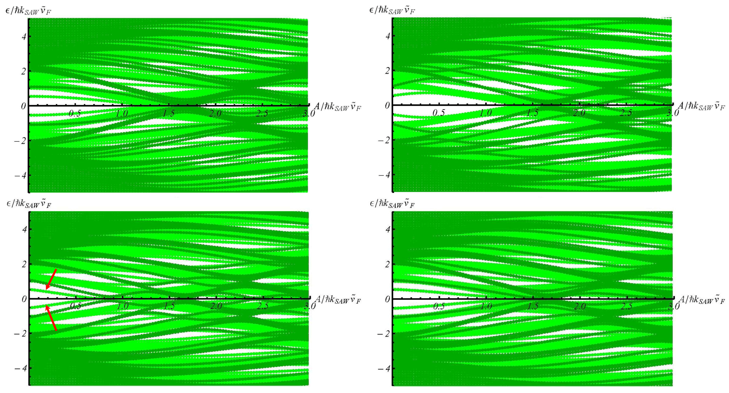
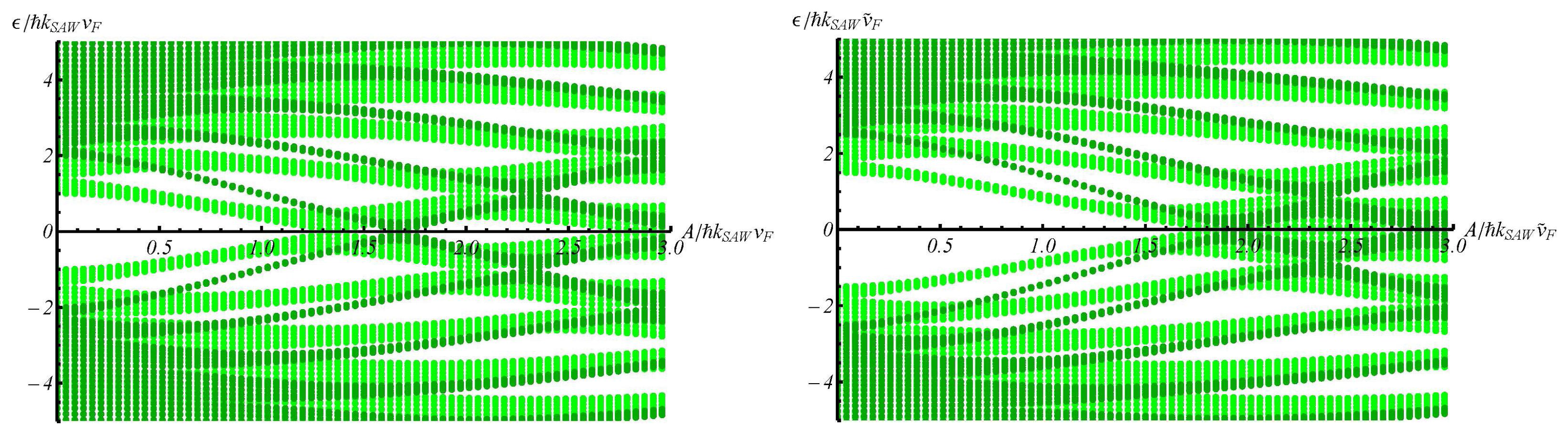
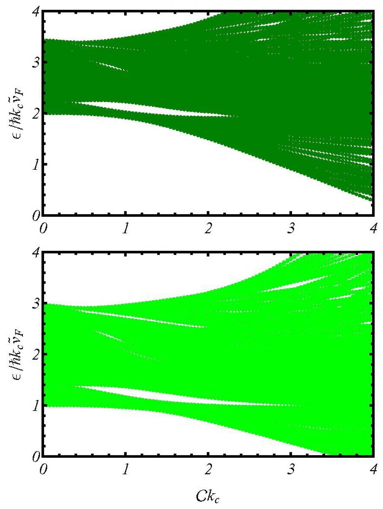
3. Numerical Simulation and Discussions

In our numerical calculations, all the energies in Figure 1 and Figure 2, such as ε, Δ and E g , are normalized to v ˜ F k S A W . The SAW potential amplitude A is also normalized to v ˜ F k S A W . Additionally, all the energies in Figure 3, such as ε and Δ, are measured in units of v ˜ F k c , and the corrugation amplitude C is normalized to 1 / k c . Besides, the transverse wave number k y ( m ) in all the plots is scaled by 2 π / 3 a 0 . In this way, we are able to draw some universal conclusions concerning the effects due to minigaps.
Figure 1. Scaled electron energy spectrum ε ( k ) / ( v ˜ F k S A W ) in the absence of electron traps as a function of the normalized SAW amplitude A / ( v ˜ F k S A W ) for semiconducting nanoribbons subjected to an acoustically induced SAW potential. In this figure, we choose Δ / ( v ˜ F k S A W ) = 1 . 0 (upper panel) and 1 . 5 (lower panel). Only the eigen-spectra arising from the two lowest dispersion curves in the absence of an SAW are displayed. Higher subbands contribute significantly at larger SAW amplitude. The lighter shaded regions arise from the lowest energy dispersion curves, whereas the darker shaded regions are associated with the energy dispersions of the next subband.
Electronics 02 00178 g001
In Figure 1, we compare the energy band structure of nanoribbons for two values of Δ in the absence of electron traps. Two values of k y ( m ) were chosen (light and dark colors) to describe the two lowest energy levels (see the discussions in the Appendix A). The minigaps are generated by a sliding dynamic QD and they oscillate as a function of the SAW amplitude A, as may be verified using perturbation theory, vanishing at values close, but generally not equal, to the roots of Bessel functions. Increasing or decreasing the value of Δ results in a shift of the nodes on the graph as evidenced by comparing our results in Figure 1. Therefore, Δ determines not only the magnitude of the original gap in the absence of an SAW but also the size of the minigaps in the presence of an SAW. Higher energy minigaps are partially closed by the energy levels corresponding to a larger value of k y ( m ) (not shown here).
Figure 2. (Color online) Scaled electron energy spectrum ε ( k ) / ( v ˜ F k S A W ) in the presence of electron traps as a function of the normalized SAW amplitude A / ( v ˜ F k S A W ) for semiconducting nanoribbons subjected to an acoustically induced SAW potential. In this figure, we chose the energy gap Δ / ( v ˜ F k S A W ) = 1 . 0 and the trap weight V 0 = V t r a p / ( v ˜ F k S A W ) = 1 . 0 for all four panels. As in Figure 1, only the eigen-spectra due to the two lowest dispersion curves in the absence of the SAW are shown. Here, the position x 0 k S A W / ( 2 π ) of electron traps, moving with the SAW potential, is located at: 1 / 3 (upper-left panel), 1 / 5 (lower-left panel), 1 / 7 (upper-right panel), and 1 / 11 (lower-right panel). Two induced trap-state energy levels within the energy gap are indicated by arrows in the lower-left panel for emphasis.
Electronics 02 00178 g002
We now introduce electron traps into our nanoribbon by superposing a negative δ-potential onto the SAW potential so as to simulate a short-range Coulomb interaction. In this case, the position of the trap is fixed in the moving SAW frame of reference, which is quite different from embedded impurities in a nanostructure. In the moving SAW frame, the embedded impurities are moving against the dynamic QDs created by both the transverse dimension of the nanostructure and the longitudinal SAW potential. This results in an average of the impurity effects with respect to these dynamic QDs in the longitudinal direction. As seen in the results presented in Figure 2, localized trap states occur within the minigaps once the weight of the trap potential V 0 becomes larger than Δ / ( v ˜ F k S A W ) . Relative energy value of these trap states in the presence of SAW is sensitive to the position x 0 of the trap within a dynamic QD. If we set λ = V 0 , then the contribution to α ( x ) from the trap located in the nodes of the SAW potential is fully compensated by the cosine term in Equation (3). As a result of this compensation, the localized trap states will disappear from the gap and minigap regions. If we extend the single-trap model employed in this letter to a uniform distribution of traps, the fluctuations in the phase term α ( x ) [see Equation (3)] would fill up the entire minigap region with a delocalized trap band. Consequently, the adiabatic approximation may not be applicable. In other words, to satisfy the adiabatic assumption, one must have dominance of the SAW potential, i.e., λ V 0 must be satisfied.
We compare the results for SAW-based dynamic QDs in Figure 1 and Figure 2 with those for static QDs created by corrugation on a graphene nanoribbon in the absence of an SAW and electron traps. We do this by displaying in Figure 3 the minigaps induced by the corrugation. We find from the figure that minigaps only exist for finite but small values of the corrugation amplitude C . This means that these minigaps are generally much less than those induced by an SAW. As a matter of fact, the existence of non-vanishing diagonal terms a n given in Equation (4) effectively mitigates the phase fluctuations in the off-diagonal terms b n . This keeps the minigaps open and the energy spectra robust even after traps have been introduced to cause a fluctuation in the phase term α c ( x ) .
Figure 3. (Color online) Minigap spectrum ε ( k ) / ( v ˜ F k c ) , induced by a corrugation potential, as a function of the normalized modulation amplitude C k c . In this figure, the two plots correspond to the two lowest values of the quantized transverse wave number k y ( m ) . The graph at the top comes from the lowest quantized energy subband, whereas the graph at the bottom is due to the first-excited subband.
Electronics 02 00178 g003
Finally, let us assume that a narrow channel is formed within a two-dimensional electron-gas layer lying in the x y -plane. We will neglect the finite thickness of the quantum well for the heterostructure in the z-direction and consider the electron motion as strictly two dimensional. We will employ one of the simplest models for the gate-induced or etched [44] confining electrostatic potential. In this way, a 1D channel is formed on the two-dimensional electron-gas layer and the dynamics of massive electrons can be modeled by a discretized 1D Schrodinger equation. However, from numerical results (not shown here), we find no evidence of the minigaps for this model, i.e., the minigaps are the characteristics of Dirac fermions.

4. Concluding Remarks

In conclusion, we have calculated in this letter the energy band structure for graphene nanoribbons, embedded with a single electron trap, upon which an SAW is launched. Our results show that localized trap states appear in the minigaps. More importantly, the location of the trap state-energy level is determined by the positions of the trap with respect to the phase of the sinusoidal SAW. Consequently, the adiabatic approximation might not be appropriate whenever the minigap is less or comparable with the weight of a short-range δ-potential for the trap (see Figure 2). On the other hand, in Figure 1, where there are no electron traps, a larger value of Δ in the energy spectrum leads to a substantial increase in the number of minigaps as well as the ballistic current quantization. Periodic corrugation of the nanoribbon may be used instead of an SAW as a mechanism for inducing minigaps. Those are expected to be less sensitive to the presence of charged impurities or electron trap potentials.

Acknowledgements

The authors are very grateful to Leonid Levitov for helpful suggestions and critical comments during the course of this work. His critical remarks have undoubtedly helped to strengthen the presentation of this letter. This research was supported by the contract # FA 9453-07-C-0207 of AFRL. DH would like to thank the Air Force Office of Scientific Research (AFOSR) for its support.

References

  1. Talyanskii, V.I.; Novikov, D.S.; Simons, B.D.; Levitov, L.S. Quantized adiabatic charge transport in a carbon nanotube. Phys. Rev. Lett. 2001, 87, 276802. [Google Scholar]
  2. Kouwenhoven, L.P.; Johnson, A.T.; van der Vaart, N. C.; Harmans, C.J.P.M.; Foxon, C.T. Quantized current in a quantum-dot turnstile using oscillating tunnel barriers. Phys. Rev. Lett. 1991, 67, 1626. [Google Scholar] [PubMed]
  3. Keller, M.W.; Eichenberger, A.L.; Martinis, J.M.; Zimmerman, N.M. A capacitance standard based on counting electrons. Science 1999, 285, 1706. [Google Scholar] [CrossRef] [PubMed]
  4. Shilton, J.M.; Talyanskii, V.I.; Pepper, M.; Ritchie, D.A.; Frost, J.E.F.; Ford, C.J.B.; Smith, C.G.; Jones, G.A.C. High-frequency single-electron transport in a quasi-one-dimensional GaAs channel induced by surface acoustic waves. J. Phys. 1996, 8, L531. [Google Scholar] [CrossRef] [PubMed]
  5. Talyanskii, V.I.; Shilton, J.M.; Pepper, M.; Smith, C.G.; Ford, C.J.B.; Linfield, E.H.; Ritchie, D.A.; Jones, G.A.C. Single-electron transport in a one-dimensional channel by high-frequency surface acoustic waves. Phys. Rev. B 1997, 56, 15180. [Google Scholar] [CrossRef]
  6. Aǐzin, G.R.; Gumbs, G.; Pepper, M. Screening of the surface-acoustic-wave potential by a metal gate and the quantization of the acoustoelectric current in a narrow channel. Phys. Rev. B 1998, 58, 10589. [Google Scholar] [CrossRef]
  7. Gumbs, G.; Aǐzin, G.R.; Pepper, M. Coulomb interaction of two electrons in the quantum dot formed by the surface acoustic wave in a narrow channel. Phys. Rev. B 1999, 60, R13954. [Google Scholar] [CrossRef]
  8. Gumbs, G.; Aǐzin, G.R.; Pepper, M. Interaction of surface acoustic waves with a narrow electron channel in a piezoelectric material. Phys. Rev. B 1998, 57, 1654. [Google Scholar] [CrossRef]
  9. Blumenthal, M.D.; Kaestner, B.; Li, L.; Giblin, S.; Janssen, T.J.B.M.; Pepper, M.; Anderson, D.; Jones, G.; Ritchie, D.A. Gigahertz quantized charge pumping. Nat. Phys. 2007, 3, 343. [Google Scholar] [CrossRef]
  10. Kaestner, B.; Kashcheyevs, V.; Amakawa, S.; Blumenthal, M.D.; Li, L.; Janssen, T.J.B.M.; Hein, G.; Pierz, K.; Weimann, T.; Siegner, U.; et al. Single-parameter nonadiabatic quantized charge pumping. Phys. Rev. B 2008, 77, 153301. [Google Scholar] [CrossRef]
  11. Thouless, D.J. Quantization of particle transport. Phys. Rev. B 1983, 27, 6083. [Google Scholar] [CrossRef]
  12. Huang, D.H.; Gumbs, G.; Pepper, M. Effects of inelastic capture, tunneling escape, and quantum confinement on surface acoustic wave-dragged photocurrents in quantum wells. J. Appl. Phys. 2008, 103, 083714. [Google Scholar] [CrossRef]
  13. Robinson, A.M.; Talyanskii, V.I. Shot noise in the current of a surface acoustic-wave-driven single electron pump. Phys. Rev. Lett. 2005, 95, 247202. [Google Scholar] [CrossRef] [PubMed]
  14. Wright, S.J.; Blumenthal, M.D.; Gumbs, G.; Thorn, A.L.T.; Holmes, S.N.; Janssen, T.J.B.M.; Pepper, M.; Anderson, D.; Jones, G.A.C.; Nicoll, C.N.; et al. Enhanced current quantization in high-frequency electron pumps in a perpendicular magnetic field. Phys. Rev. B 2008, 78, 233311. [Google Scholar] [CrossRef]
  15. Wright, S.J.; Thorn, A.L.; Blumenthal, M.D.; Giblin, S.P.; Pepper, M.; Janssen, T.J.B.M.; Kataoka, M.; Fletcher, J.D.; Jones, G.A.C.; Nicoll, C.A.; Gumbs, G.; Ritchie, D.A. Single- and few-electron dynamic quantum dots in a perpendicular magnetic field. J. Appl. Phys. 2011, 109, 102422. [Google Scholar] [CrossRef]
  16. Neto, A.H.C.; Guinea, F.; Peres, N.M.R.; Novoselov, K.S.; Geim, A.K. The electronic properties of graphene. Rev. Mod. Phys. 2009, 81, 109–162. [Google Scholar] [CrossRef]
  17. Special issue on Electronic and Photonic Properties of Graphene Layers and Carbon Nanoribbons. Gumbs, G.; Huang, D.H.; Roslyak, O. (Eds.) Philos. Trans. R. Soc. Lodon, Ser. A, 2010; 138, No. 1932.
  18. Abergel, D.S.L.; Apalkov, V.; Berashevich, J.; Ziegler, K.; Chakraborty, T. Properties of graphene: A theoretical perspective. Adv. Phys. 2010, 59, 261–482. [Google Scholar] [CrossRef]
  19. Orlita, M.; Potemski, M. Dirac electronic states in graphene systems: Optical spectroscopy studies. Semicond. Sci. Technol. 2010, 25, 063001. [Google Scholar] [CrossRef]
  20. Das Sarma, S.; Adam, S.; Hwang, E.H.; Rossi, E. Electronic transport in two-dimensional graphene. Rev. Mod. Phys. 2011, 83, 407–470. [Google Scholar] [CrossRef]
  21. Novoselov, K.S.; Geim, A.K.; Morozov, S.V.; Jiang, D.; Katsnelson, M.I.; Grigorieva, I.V.; Dubonos, S.V.; Firsov, A.A. Electric field effect in atomically thin carbon films. Science 2001, 306, 666–669. [Google Scholar] [CrossRef] [PubMed]
  22. Novoselov, K.S.; Geim, A.K.; Morozov, S.V.; Jiang, D.; Katsnelson, M.I.; Grigorieva, I.V.; Dubonos, S.V.; Firsov, A.A. Two-dimensional gas of massless Dirac fermions in graphene. Nature 2005, 438, 197–200. [Google Scholar] [CrossRef] [PubMed] [Green Version]
  23. Zhang, Y.; Tan, Y.-W.; Störmer, H.L.; Kim, P. Experimental observation of the quantum Hall effect and Berry’s phase in graphene. Nature 2005, 438, 201–204. [Google Scholar] [CrossRef] [PubMed]
  24. Katsnelson, M.I.; Novoselov, K.S.; Geim, A.K. Chiral tunnelling and the Klein paradox in graphene. Nat. Phys. 2006, 2, 620–625. [Google Scholar] [CrossRef] [Green Version]
  25. Young, A.F.; Kim, P. Quantum interference and Klein tunnelling in graphene. Nat. Phys. 2009, 5, 222–226. [Google Scholar] [CrossRef]
  26. Roslyak, O.; Iurov, A.; Gumbs, G.; Huang, D.H. Unimpeded tunneling in graphene nanoribbons. J. Phys. 2010, 22, 165301. [Google Scholar] [CrossRef] [PubMed]
  27. Iurov, A.; Gumbs, G.; Roslyak, O.; Huang, O.H. Anomalous photon-assisted tunneling in graphene. J. Phys. 2012, 24, 015303. [Google Scholar] [CrossRef] [PubMed]
  28. Wunsch, B.; Stauber, T.; Sols, F.; Guinea, F. Dynamical polarization of graphene at finite doping. New J. Phys. 2006, 8, 318. [Google Scholar] [CrossRef]
  29. Wang, E.H.; Das Sarma, S. Dielectric function, screening, and plasmons in two-dimensional graphene. Phys. Rev. B 2007, 75, 205418. [Google Scholar] [CrossRef]
  30. Roslyak, O.; Gumbs, G.; Huang, D.H. Plasma excitations of dressed Dirac electrons in graphene layers. J. Appl. Phys. 2011, 109, 113721. [Google Scholar] [CrossRef]
  31. Mak, K.F.; Sfeir, M.Y.; Wu, Y.; Lui, C.H.; Misewich, J.A.; Heinz, T.F. Measurement of the optical conductivity of graphene. Phys. Rev. Lett. 2008, 101, 196405. [Google Scholar] [CrossRef] [PubMed]
  32. Nair, R.R.; Blake, P.; Grigorenko, A.N.; Novoselov, K.S.; Booth, T.J.; Stauber, T.; Peres, N.M.R.; Geim, A.K. Fine structure constant defines visual transparency of graphene. Science 2008, 320, 1308. [Google Scholar] [CrossRef] [PubMed]
  33. Ju, L.; Geng, B.; Horng, J.; Girit, C.; Martin, M.; Hao, Z.; Bechtel, H.A.; Liang, H.A.; Zettl, A.; Shen, Y.R.; et al. Graphene plasmonics for tunable terahertz metamaterials. Nat. Nanotechnol. 2011, 6, 630–634. [Google Scholar] [CrossRef] [PubMed]
  34. Huang, D.H.; Gumbs, G.; Roslyak, O. Effects of nonlocal plasmons in coupled gapped graphene micro-ribbon array and two-diemnsional electron gas on near-field electromagnetic response in the deep-subwavelength regime. Appl. Opt. 2013, 52, 755–769. [Google Scholar] [CrossRef] [PubMed]
  35. Li, Z.Q.; Henriksen, E.A.; Jiang, Z.; Hao, Z.; Martin, M.C.; Kim, P.; Störmer, H.L.; Basov, D.N. Dirac charge dynamics in graphene by infrared spectroscopy. Nat. Phys. 2008, 4, 532–535. [Google Scholar] [CrossRef]
  36. Wang, F.; Zhang, Y.; Tian, C.; Girit, C.; Zettl, A.; Crommie, M.; Shen, Y.R. Gate-variable optical transitions in graphene. Science 2008, 320, 206–209. [Google Scholar] [CrossRef]
  37. Bao, Q.; Zhang, H.; Wang, B.; Ni, Z.; Haley, C.; Lim, Y.X.; Wang, Y.; Tang, D.Y.; Loh, K.P. Broadband graphene polarizer. Nat. Photonics 2011, 5, 411–415. [Google Scholar] [CrossRef]
  38. Strait, J.H.; Wang, H.; Shivaraman, S.; Shields, V.; Spencer, M.; Rana, F. Hot carrier transport and photocurrent response in graphene. Nano Lett. 2011, 11, 4688–4692. [Google Scholar]
  39. Song, J.C.W.; Rudner, M.S.; Marcus, C.M.; Levitov, L.S. Very slow cooling dynamics of photoexcited carriers in graphene observed by optical-pump terahertz-probe spectroscopy. Nano Lett. 2011, 11, 4902–4906. [Google Scholar]
  40. Roslyak, O.; Gumbs, G.; Huang, D.H. Tunable band structure effects on ballistic transport in graphene nanoribbons. Phys. Lett. A 2010, 374, 4061–4064. [Google Scholar]
  41. Huang, D.H.; Gumbs, G.; Roslyak, O. Field enhanced mobility by nonlinear phonon scattering of Dirac electrons in semiconducting graphene nanoribbons. Phys. Rev. B 2011, 83, 115405. [Google Scholar]
  42. Roslyak, O.; Gumbs, G.; Huang, D.H. Energy loss spectroscopy of epitaxial versus free-standing multilayer graphene. Phys. E 2012, 44, 1874–1884. [Google Scholar]
  43. Cox, J.D.; Singh, M.R.; Gumbs, G.; Anton, M.A.; Carreno, F. Dipole-dipole interaction between a quantum dot and a graphene nanodisk. Phys. Rev. B 2012, 86, 125452. [Google Scholar] [CrossRef]
  44. Cunningham, J.; Talyanskii, V.I.; Shilton, J.M.; Pepper, M. Single-electron acoustic charge transport on shallow-etched channels in a perpendicular magnetic field. Phys. Rev. B 2000, 62, 1564. [Google Scholar] [CrossRef]
  45. Atanasov, V.; Saxena, A. Tuning the electronic properties of corrugated graphene: Confinement, curvature, and band-gap opening. Phys. Rev. B 2010, 81, 205409. [Google Scholar] [CrossRef]

A. Energy Band Calculations in Absence of Electron Traps

A.1. Carbon Nanotubes

The electron eigenstates in a semi-metallic nanotube are described by a 1D Dirac equation. For simplicity, a non-interacting system is considered here. Under the stationary approximation, the single particle energy spectrum ε ( k ) is obtained from the following perturbed 1D Dirac equation
ε ( k ) ψ α ( x ) = - i v ˜ F ψ α ( x ) x + Δ ψ β ( x ) + A sin ( k x ) ψ α ( x ) ,
ε ( k ) ψ β ( x ) = i v ˜ F ψ β ( x ) x + Δ ψ α ( x ) + A sin ( k x ) ψ β ( x ) .
In this notation, k represents the electron wave number along the nanotube, v ˜ F is the Fermi velocity of Dirac electrons, A is the SAW amplitude, Δ is the energy gap of the system in the absence of an SAW, α and β label the two sublattices of graphene from which the nanotube is rolled. In addition, we require k = k S A W to satisfy momentum conservation, where k S A W is the wave number of an SAW propagating along the nanotube. To explore the miniband structure due to quantum confinement in the radial direction, a gauge transformation is implemented and is defined by
ψ α ( x ) ψ β ( x ) = e ( i / 2 ) σ ^ 3 λ cos ( k x ) ψ α ( x ) ψ β ( x ) = e ( i / 2 ) λ cos ( k x ) ψ β ( x ) e ( - i / 2 ) λ cos ( k x ) ψ α ( x ) ,
where λ = 2 A / ( v ˜ F k ) is the normalized SAW amplitude. Substituting Equation (7) into Equations (5) and (6), we obtain
ε ( k ) e ( i / 2 ) λ cos ( k x ) ψ β ( x ) = - i v ˜ F x e ( i / 2 ) λ cos ( k x ) ψ β ( x ) + Δ e ( - i / 2 ) λ cos ( k x ) ψ α ( x ) + A sin ( k x ) e ( i / 2 ) λ cos ( k x ) ψ β ( x ) ,
ε ( k ) e ( - i / 2 ) λ cos ( k x ) ψ α ( x ) = i v ˜ F x e ( - i / 2 ) λ cos ( k x ) ψ α ( x ) + Δ e ( i / 2 ) λ cos ( k x ) ψ β ( x ) + A sin ( k x ) e ( - i / 2 ) λ cos ( k x ) ψ α ( x ) .
By introducing the following identities
- i v ˜ F x e ( i / 2 ) λ cos ( k x ) ψ β ( x ) = - A sin ( k x ) ψ β ( x ) - i v ˜ F e ( i / 2 ) λ cos ( k x ) ψ β ( x ) x ,
i v ˜ F x e ( - i / 2 ) λ cos ( k x ) ψ α ( x ) = - A sin ( k x ) ψ α ( x ) + i v ˜ F e ( - i / 2 ) λ cos ( k x ) ψ α ( x ) x ,
Equations (9) and (A.1) may be simplified as
ε ( k ) ψ β ( x ) = - i v ˜ F ψ β ( x ) x + Δ e - i λ cos ( k x ) ψ α ( x ) ,
ε ( k ) ψ α ( x ) = i v ˜ F ψ α ( x ) x + Δ e i λ cos ( k x ) ψ β ( x ) .
Furthermore, by employing the basis set Ψ ^ ( x ) ψ α ( x ) , ψ β ( x ) , the above equations can be rewritten into a compact matrix form, given by
ε ( k ) I ^ Ψ ^ ( x ) = H ^ Ψ ^ ( x ) ,
H ^ = i v ˜ F σ 3 ^ x + Δ σ ^ 1 e - i λ σ ^ 3 cos ( k x ) .
We will solve the eigenvalue problem within the spatial interval 0 < x < 2 π / k and introduce the N-point mesh x n = n δ x , where n 0 N - 1 and δ x = 2 π / k N . In this way, the derivative on the mesh can be approximated by Ψ ^ ( x n ) / x [ Ψ ^ ( x n + 1 ) - Ψ ^ ( x n - 1 ) ] / ( 2 δ x ) . Especially, on this spatial mesh, the Hamiltonian in Equation (15) may be projected into the matrix given in Equation (1).

A.2. Graphene Nanoribbons

Here, we consider an armchair graphene nanoribbon lying along the x-direction. The total number of carbon atoms (in both sublattices) across the ribbon is assumed to be M. The armchair edges mix up the graphene K and K valleys so that the wave function becomes
Ψ ^ m ( x , y ) = e i k y ( m ) y Ψ ^ K , m ( x ) + e - i k y ( m ) y Ψ ^ K , m ( x ) ,
where the transverse wave number is given by
k y ( m ) = 2 π m 2 L + a 0 + 2 π 3 a 0 ,
m = 0 , ± 1 , ± 2 , is an integer, L is the nanoribbon width, and a 0 = 3 a / 2 ( a 1 . 42 Å) is the size of the unit cell in graphene. Nanoribbons with width L / a 0 = 3 M + 1 give rise to the following relation
k y ( m ) = 2 π m 6 M a 0 + 3 a 0 + 2 π 3 a 0 = 2 π 3 a 0 2 M + 1 + m 2 M + 1 ,
and it is clear that the minimum energy occurs at k y ( - 2 M - 1 ) = 0 . Therefore, such nanoriibons are metallic. The next miniband corresponds to k y ( - 2 M ) = ( 2 π / 3 a 0 ) [ 1 / ( 2 M + 1 ) ] . On the other hand, for nanoriibons having width L / a 0 = 3 M (upper Equation) or L / a 0 = 3 M - 1 (lower Eq.), the two minimal values of k y ( m ) are found to be
k y ( - 2 M ) = ( 2 π / 3 a 0 ) [ 1 / ( 6 M + 1 ) ] and k y ( - 2 M - 1 ) = ( 2 π / 3 a 0 ) [ - 2 / ( 6 M + 1 ) ] , k y ( - 2 M ) = ( 2 π / 3 a 0 ) [ - 1 / ( 6 M - 1 ) ] and k y ( - 2 M + 1 ) = ( 2 π / 3 a 0 ) [ 2 / ( 6 M - 1 ) ] .
Those nanoribbons are semiconducting with the energy gap determined by
Δ ( M ) = 2 π v ˜ F 3 a 0 1 6 M ± 1 .
The x-component of the wave function in Equation (16) may be determined by
ε ( k ) I ^ Ψ ^ K ( K ) , m ( x ) = H ^ Ψ ^ K ( K ) , m ( x ) ,
H ^ = ± v ˜ F - i σ ^ 1 x + i k y ( m ) σ ^ 2 + A sin ( k x ) I ^ ,
where the ± signs correspond to K and K valleys. Additionally, the Hamiltonian in Equation (22) can be transformed into the form in Equation (15) after applying the following unitary transformation
U ^ = e - i α ( x ) - e i α ( x ) e - i α ( x ) e i α ( x ) ,
where α ( x ) = - A cos ( k S A W x ) / ( v ˜ F k S A W ) . As a result, the transformed Hamiltonian takes the form
H ^ = U ^ H ^ U ^ = ± v ˜ F - i / x - i k y ( m ) e i 2 α ( x ) i k y ( m ) e - i 2 α ( x ) i / x .
Formally, this Hamiltonian is equivalent to that in Equation (15) after we apply the following substitutions:
2 α ( x ) - λ cos ( k S A W x ) v ˜ F k y ( m ) Δ .
The valley sign ± does not change anything due to the mirror symmetry in the energy dispersion relation ε ( k ) with respect to ± k .

A.3. Corrugated Nanoribbons

We now turn to the case of a corrugated graphene nanoribbon whose modulation is sinusoidal with amplitude C and wavelength 2 π / k c along the x-axis. The model Hamiltonian for such a corrugated graphene nanoribbon has been given in [45] as
H ^ = - i v ˜ F σ 1 ^ x + v ˜ F k y σ 2 ^ - i v ˜ F σ 1 ^ K ( x ) 2 d f ( x ) / d x Δ c ( x ) ,
where
Δ c ( x ) = 1 + [ d f ( x ) / d x ] 2 and K ( x ) = - d 2 f ( x ) / d x 2 1 + [ d f ( x ) / d x ] 2 , f ( x ) = C sin ( k c x ) .
After applying the following unitary transformation
U ^ = 1 2 e - i α c ( x ) - e i α c ( x ) e - i α c ( x ) e i α c ( x ) and U ^ = 1 2 e i α c ( x ) e i α c ( x ) - e - i α c ( x ) e - i α c ( x ) ,
where
α c ( x ) = C 2 k c 3 4 0 x d u sin 2 k c u 1 + C 2 k c 2 cos 2 k c u 3 / 2 = 1 2 2 2 + C 2 k c 2 cos 2 k c x + C 2 k c 2 - 1 1 + C 2 k c 2 ,
the transformed Hamiltonian becomes
H ^ = v ˜ F G ( x ) - i / x Δ c ( x ) - i k y e 2 i α c ( x ) i k y e - 2 i α c G * ( x ) + i / x Δ c ( x ) ,
where the complex function is defined by
G ( x ) = - 2 C 2 k c 3 sin ( 2 k c x ) Δ c ( x ) 2 + C 2 k c 2 cos ( 2 k c x ) + C 2 k c 2 3 / 2 + i C 2 k c 3 4 Δ c 3 ( x ) sin ( 2 k c x ) .
By making use of the finite-difference method for calculating / x along with the following basis set
φ = A n - 1 , B n - 1 , A n , B n , A n + 1 , B n + 1 ,
the transformed Hamiltonian matrix in Equation (27) may be projected as
H ^ = v ˜ F G ( x n - 1 ) - i k y e 2 i α c ( x n - 1 ) - i Δ c ( x n - 1 ) 2 δ x 0 0 0 i k y e - 2 i α c ( x n - 1 ) G * ( x n - 1 ) 0 i Δ c ( x n - 1 ) 2 δ x 0 0 i Δ c ( x n ) 2 δ x 0 G ( x n ) - i k y e 2 i α c ( x n ) - i Δ c ( x n ) 2 δ x 0 0 - i Δ c ( x n ) 2 δ x i k y e - 2 i α c ( x n ) G * ( x n ) 0 i Δ c ( x n ) 2 δ x 0 0 i Δ c ( x n + 1 ) 2 δ x 0 G ( x n + 1 ) - i k y e 2 i α c ( x n + 1 ) 0 0 0 - i Δ c ( x n + 1 ) 2 δ x i k y e - 2 i α c ( x n + 1 ) G * ( x n + 1 ) .
The above Hamiltonian matrix has the same form as Equation (1).

