Far Field Extrapolation from Near Field Interactions and Shielding Influence Investigations Based on a FE-PEEC Coupling Method

Abstract
:1. Introduction
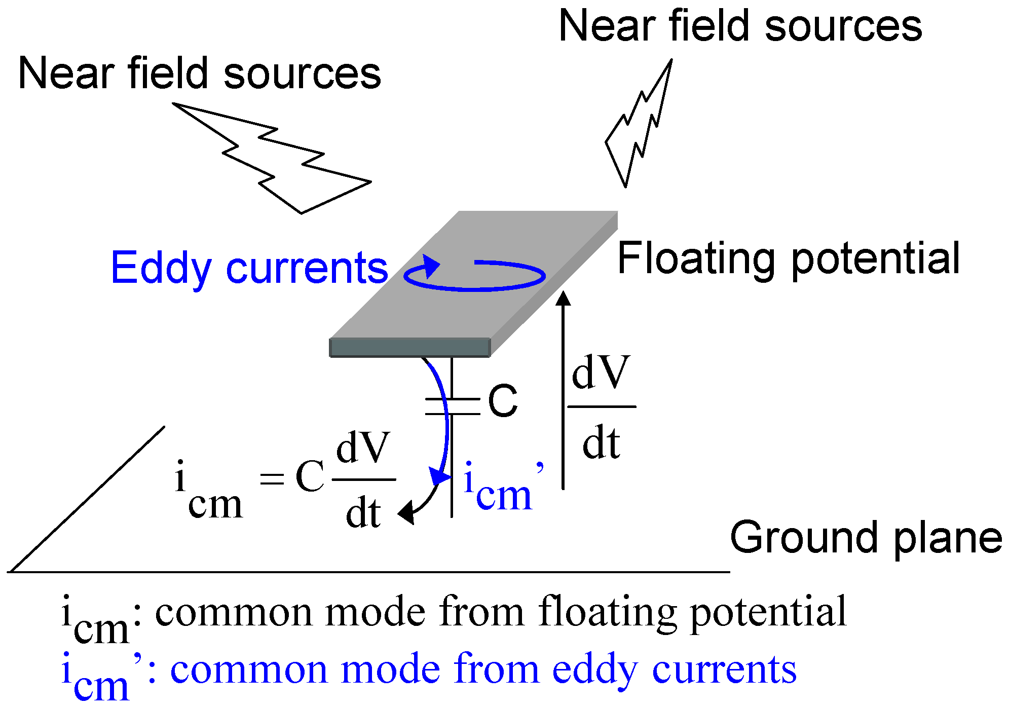
2. EMC Study of Static Converters
3. State of the Art on Modeling Methods
3.1. Usual Methods
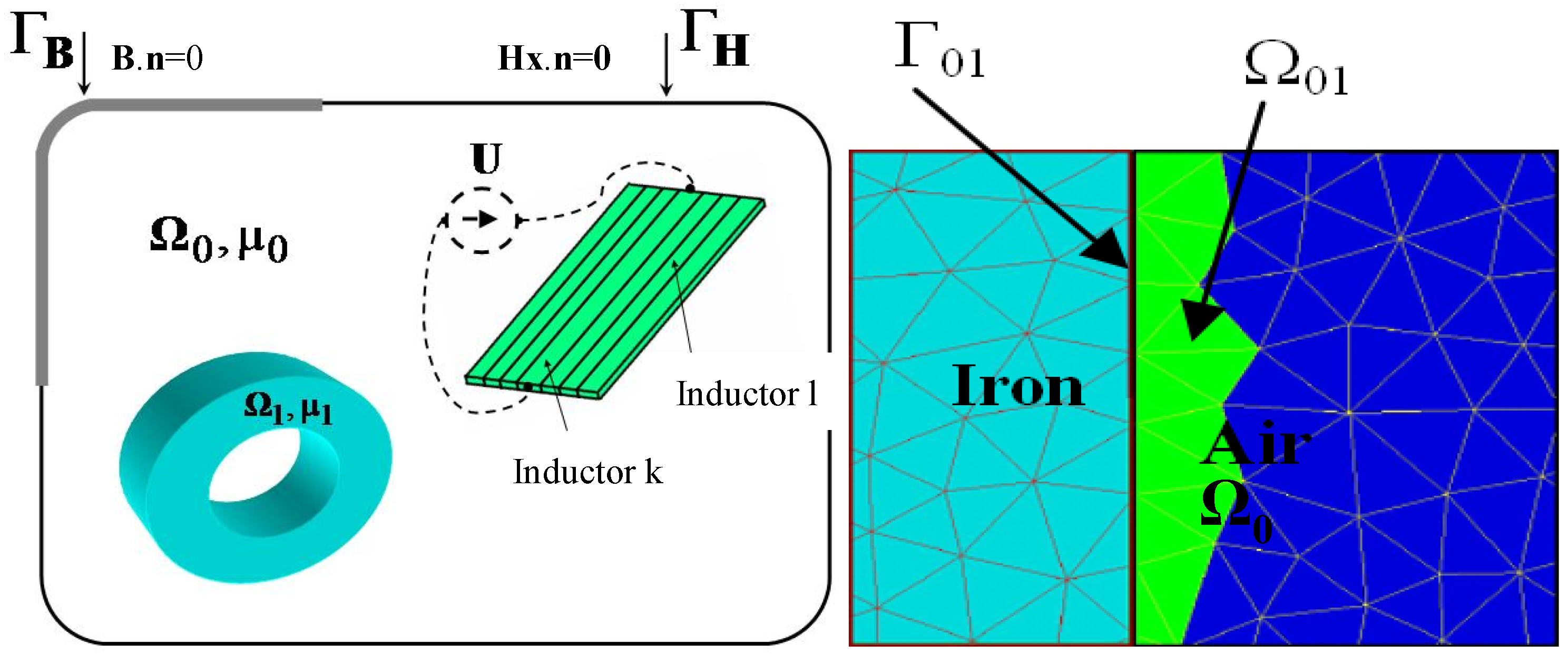
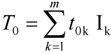
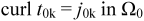
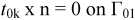
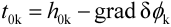
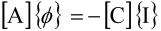
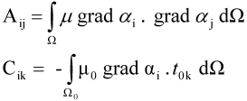
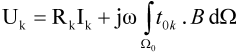
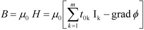
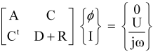
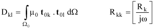
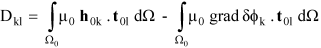
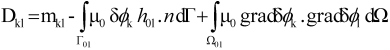
3.2. Hybrid Method
- Close to the conductors, variations of magnetic field is very important [19], so to take this aspect into account, the meshing must be dense;
- Geometry of conductors is very hard to mesh with a good quality since it can be constituted by very this planes like DBC (Direct Copper Board).
- PEEC method easily takes into account interactions between complex 3D massive conductors;
- FEM takes the interaction between conductors and ferromagnetic materials into account.
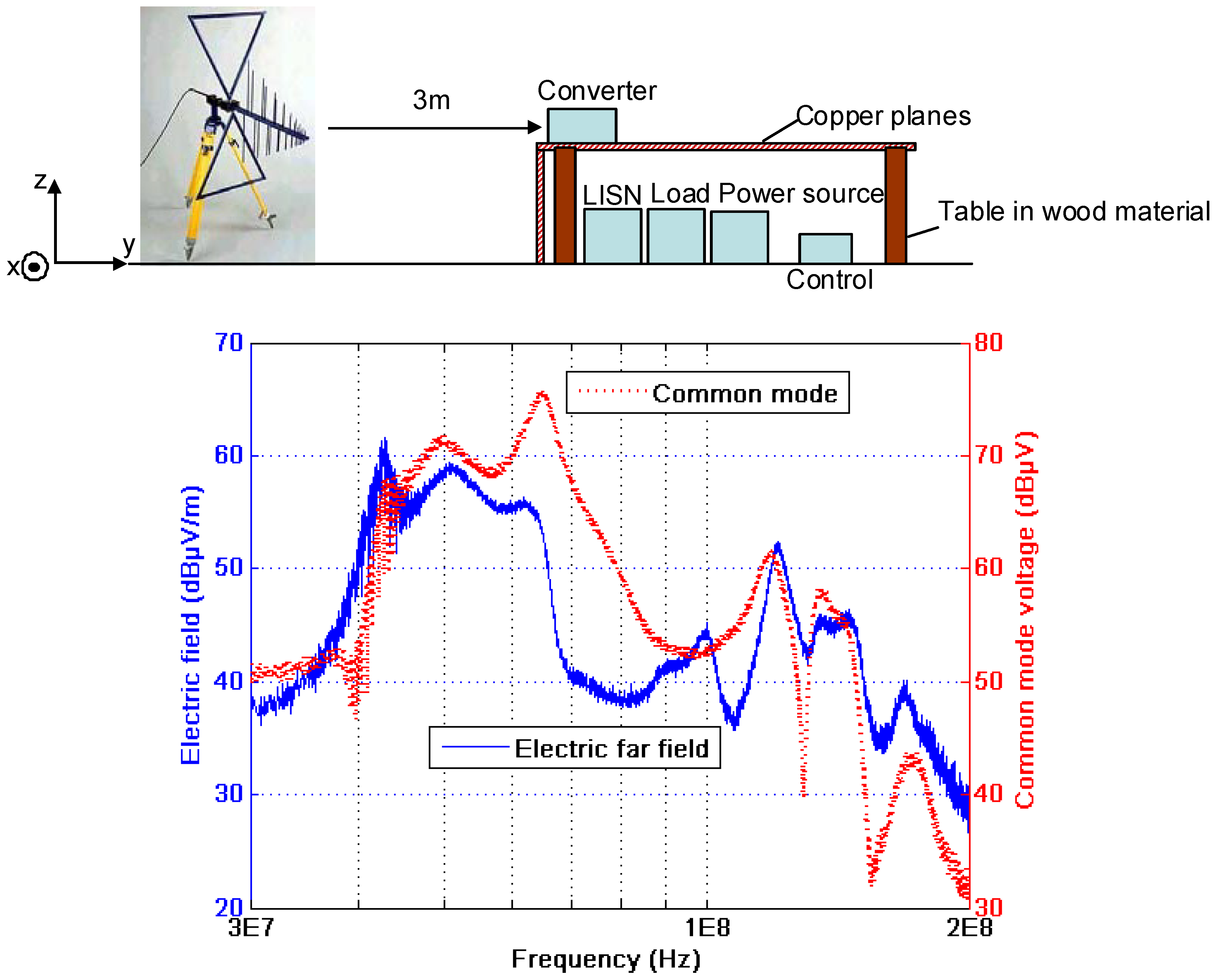
4. Application and Results
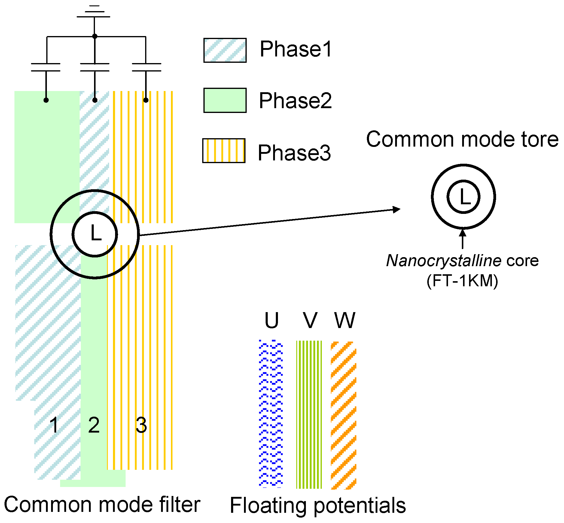
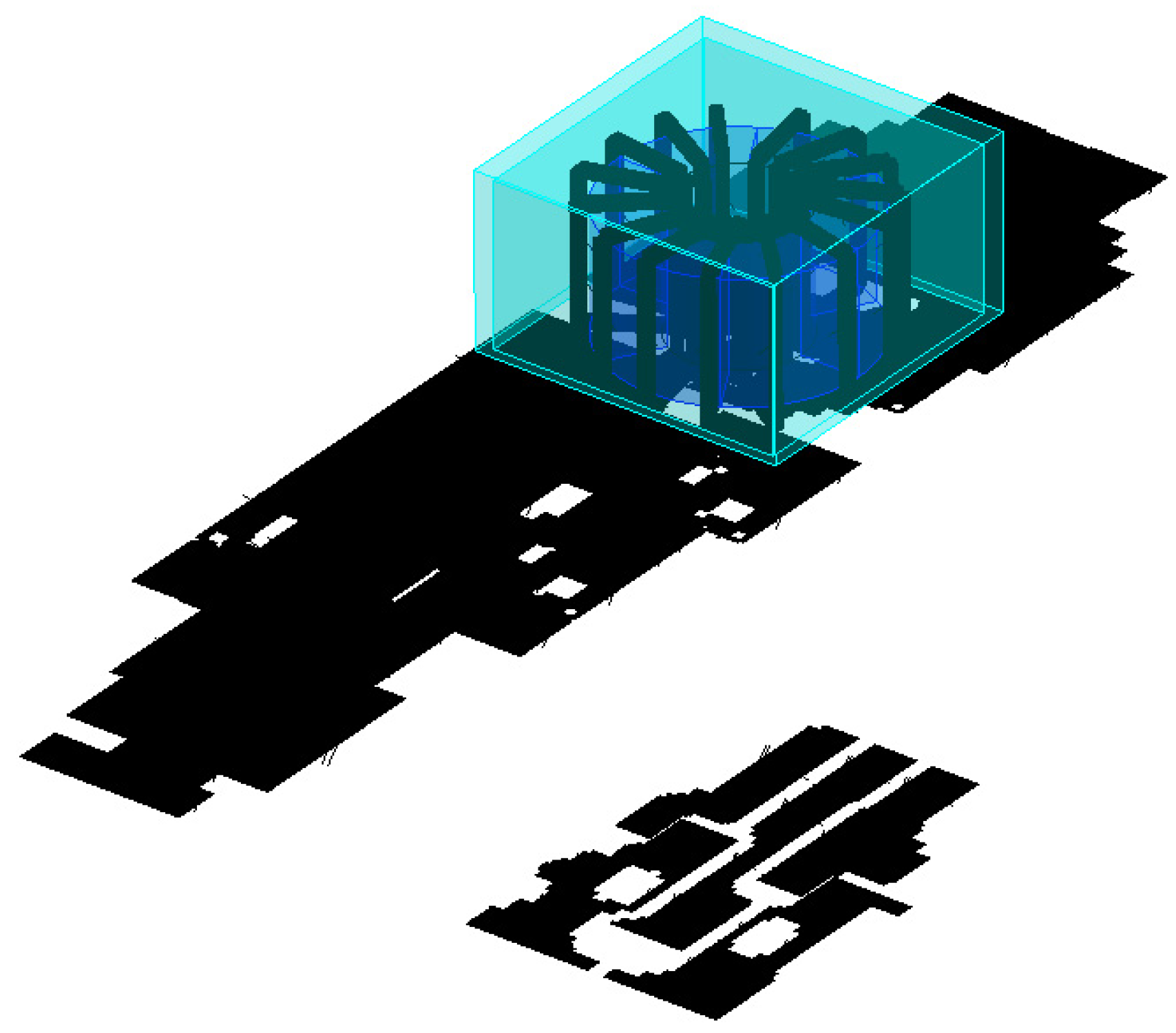
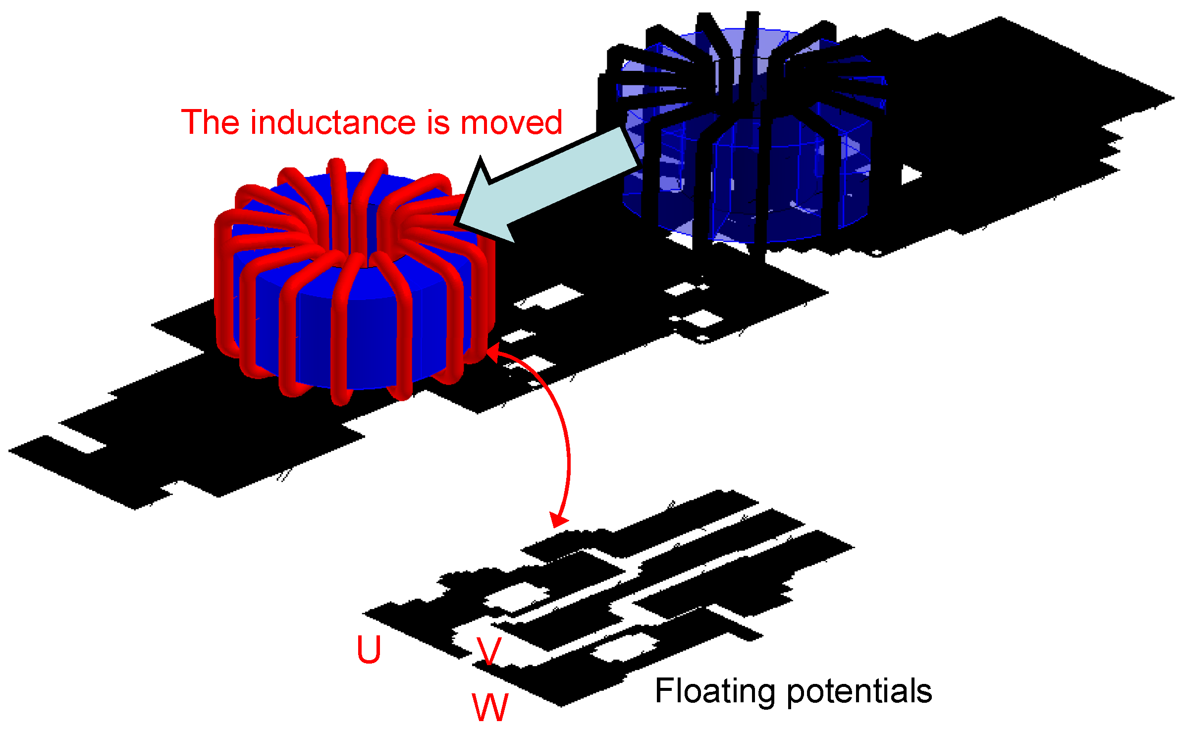
4.1. Studied Structure
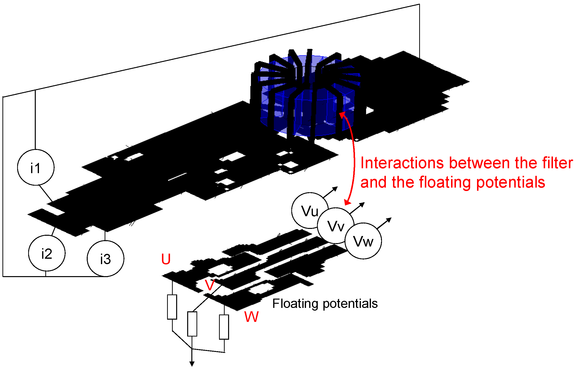
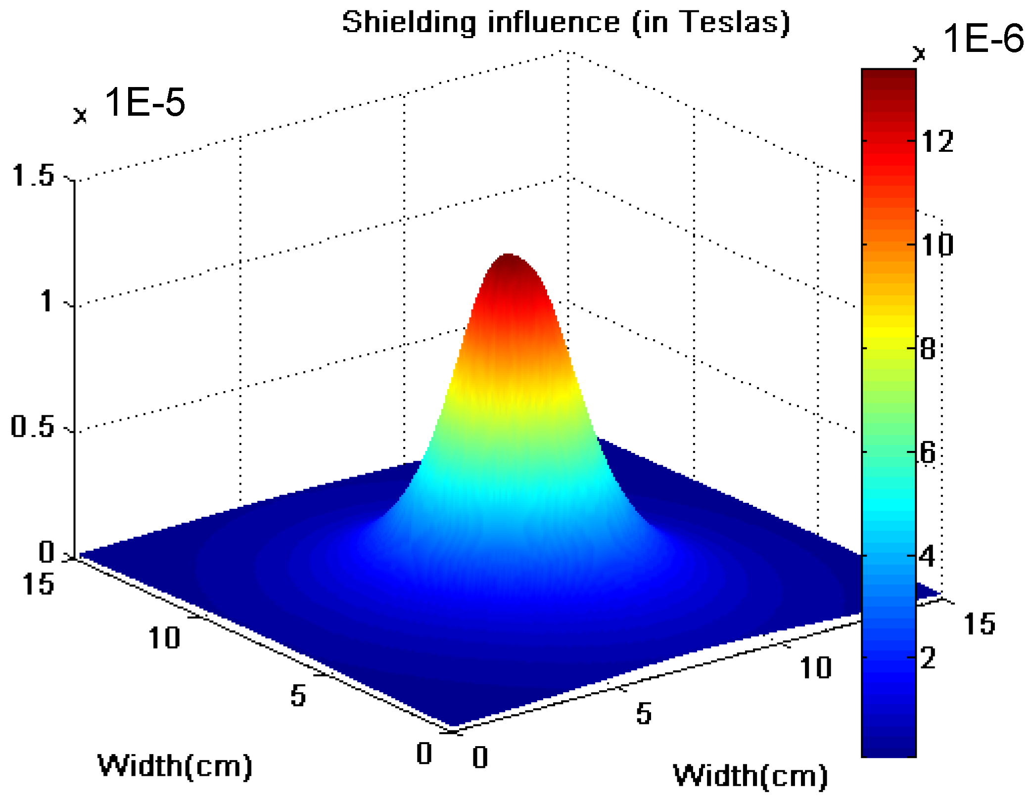
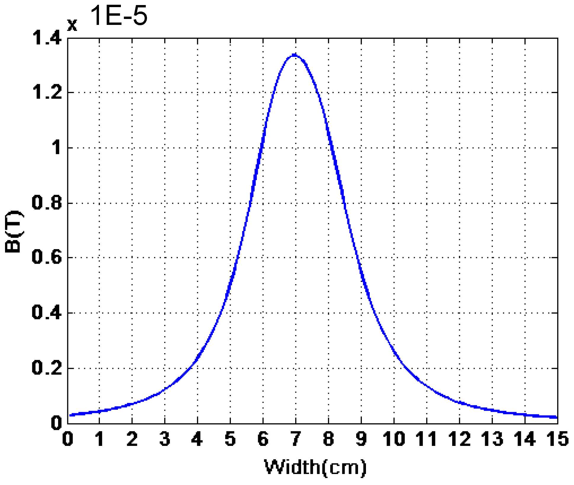
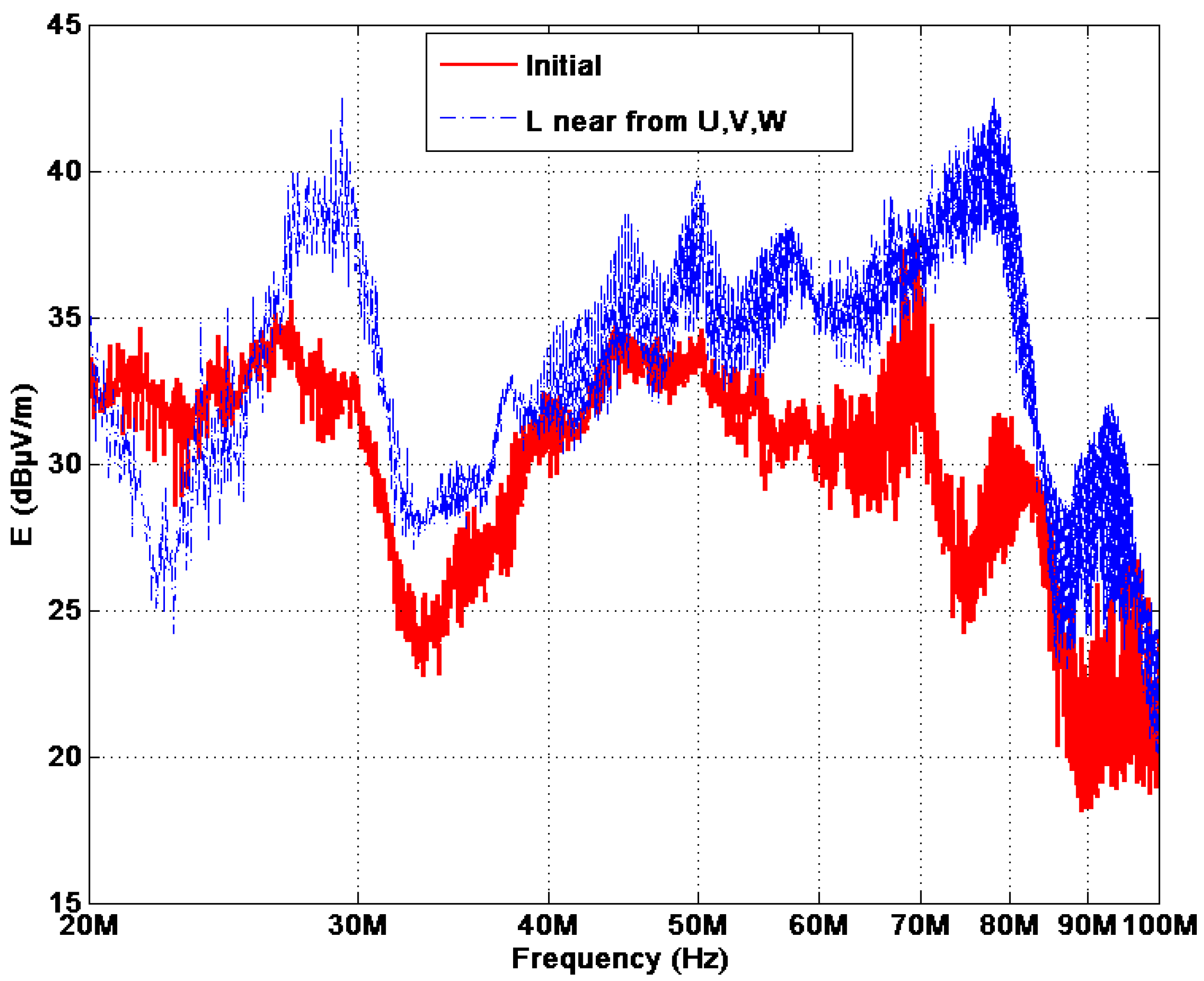
4.2. Results

| Currents without filter (A) | U | V | W |
| 328.628 | 373.487 | 403.316 | |
| Currents with filter (A) | U | V | W |
| Without shielding (A) | 465.60 | 527.09 | 570.53 |
| With shielding (A) | 465.59 | 527.04 | 570.48 |

4.3. Conclusions
5. Conclusion
References
- Wu, M.K.; Tse, C.K. Development of an integrated CAD tool for switching power supply design with EMC performance evaluation. IEEE Trans. Ind. Appl. 1998, 34, 364–373. [Google Scholar] [CrossRef]
- Nagesware Rao, K.; Venkata Ramana, P. EMC analysis in PCB designs using and expert system. Int. Conf. EMI EMC 1995, 59–62. [Google Scholar]
- Xin, W.; Pong, M.H.; Lee, C.M.; Qian, Z.M. Reduction of EMI by Electric Field Method. In Proceedings of the Fourteenth Annual Applied Power Electronics Conference and Exposition, Dallas, TX, USA, March 1999; pp. 135–138.
- Xin, W.; Pong, M.H.; Lee, C.M.; Qian, Z.M. A Novel Approach Base on Electric Field Analysis to Reduce Crosstalk Problem on PCB. In Proceedings of the 30th Annual IEEE Power Electronics Specialists Conference, Charleston, SC, USA, March 1999; pp. 845–849.
- Sroka, J. On the coupling of the generalized multipole technique with the finite element method. IEEE Trans. Magn. 1990, 26, 658–661. [Google Scholar] [CrossRef]
- Jin, J.-M.; Volakis, J.L.; Collins, J.D. A finite-element_boundary-integral method for scattering and radiation by two- and three-dimensional structures. IEEE Antennas Propag. Mag. 1991, 33, 22–32. [Google Scholar]
- Tran, T.-S.; Meunier, G.; Labie, P.; Le Floch, Y.; Roudet, J.; Guichon, J.-M.; Roudet, J.; Maréchal, Y. Coupling PEEC-Finite element method for solving electromagnetic problem. IEEE Trans. Magn. 2008, 44, 1330–1333. [Google Scholar] [CrossRef]
- Mutoh, N.; Ogata, M.; Gulez, K.; Harashima, F. New methods to suppress emi noises in motor drive systems. IEEE Trans. Ind. Electron. 2002, 49, 474–485. [Google Scholar] [CrossRef]
- Mutoh, N.; Nakashima, J.; Kanesaki, M. Multilayer power printed structures suitable for controlling emi noises generated in power converters. IEEE Trans. Ind. Electron. 2003, 50, 1085–1094. [Google Scholar] [CrossRef]
- Aimé, J.; Roudet, J.; Vollaire, C.; Baudesson, P.; Ecrabey, J. Layout Techniques for Reduction of Common Mode Current in Static Converters. In Proceedings of the 2006 IEEE Industry Applications Conference (41st IAS Annual meeting), Tampa, FL, USA, October 2006; pp. 2296–2303.
- Aimé, J.; Clavel, E.; Roudet, J.; Meunier, G.; Loizelet, P. Electromagnetic Modelling Process to Improve Cabling of Power Electronic Structures. In Proceedings of the ISEF 2009 XIV International Symposium on Electromagnetic Fields in Mechatronics, Electrical and Electronic Engineering, Arras, France, 10–12 September 2009; [CD-ROM]. Artois Presse Université: Arras Cedex, France, 2009. [Google Scholar]
- Yutaka, I.; Tadao, K. Shielding Method of Printed Circuit Board and Device Mounted Printed Board Using this Method. Japanese Patent 2 003078279 A, 14 March 2003. [Google Scholar]
- CEDRAT Company Homepage. Available online: http://www.cedrat.com (accessed on 10 October 2011).
- Paul, C.R. A comparison of the contributions of common mode and differential mode currents in radiated emissions. IEEE Trans. Electromagn. Compat. 1989, 31, 189–193. [Google Scholar] [CrossRef]
- Vincent, B.; Chadebec, O.; Schanen, J.L. Multipolar expansion sensors for near field characterization. In Proceedings of the 2008 International Symposium on Electromagnetic Compatibility, Hamburg, Germany, September 2008; pp. 1–4.
- Harrington, R.F. Field Computation by Moment Methods; The Macmillan Company: New York, NY, USA, 1968. [Google Scholar]
- Ruehli, A.E. Inductance calculations in a complex integrated circuit environment. IBM J. Res. Develop. 1972, 16, 470–481. [Google Scholar] [CrossRef]
- Cangellaris, A.C. Frequency-Domain Finite Element Methods for Electromagnetic Field Simulation: Fundamentals, State of the Art, and Applications to EMI/EMC Analysis. In Proceedings of the 1996 IEEE International Symposium on Electromagnetic Compatibility, Santa Clara, CA, USA, August 1996; pp. 107–116.
- Aimé, J.; Tran, T.-S.; Clavel, E.; Meunier, G.; Le Floch, Y.; Baudesson, P. Magnetic field computation of a common mode filter using finite element, PEEC methods and their coupling. In Proceedings of the 2008 IEEE International Symposium on Industrial Electronics, Cambridge, UK, 30 June–2 July 2008; pp. 7–12.
- Simkin, J.; Trowbridge, C.W. On the use of the total scalar potential in the numerical solution of field problems in electromagnetics. Int. J. Numer. Methods Eng. 1979, 14, 423–440. [Google Scholar] [CrossRef]
- Biro, O.; Preis, K.; Buchgraber, G.; Ticar, I. Voltage driven coils in finite-element formulations using a current vector and a magnetic scalar potential. IEEE Trans. Magn. 2004, 40, 1286–1289. [Google Scholar] [CrossRef]
- Mayergoyz, I.D.; Bedrosian, G. On calculation of 3-D eddy currents in conducting and magnetic shells. IEEE Trans. Magn. 1995, 31, 1319–1324. [Google Scholar] [CrossRef]
- Guérin, C.; Meunier, G. 3-D Magnetic Scalar Potential Finite Element Formulation for Conducting Shells Coupled With an External Circuit. IEEE Trans. Magn. 2012, 48, 323–326. [Google Scholar] [CrossRef]
© 2013 by the authors; licensee MDPI, Basel, Switzerland. This article is an open access article distributed under the terms and conditions of the Creative Commons Attribution license (http://creativecommons.org/licenses/by/3.0/).
Share and Cite
Clavel, E.; Tran, T.-S.; Aimé, J.; Meunier, G.; Roudet, J. Far Field Extrapolation from Near Field Interactions and Shielding Influence Investigations Based on a FE-PEEC Coupling Method. Electronics 2013, 2, 80-93. https://doi.org/10.3390/electronics2010080
Clavel E, Tran T-S, Aimé J, Meunier G, Roudet J. Far Field Extrapolation from Near Field Interactions and Shielding Influence Investigations Based on a FE-PEEC Coupling Method. Electronics. 2013; 2(1):80-93. https://doi.org/10.3390/electronics2010080
Chicago/Turabian StyleClavel, Edith, Thanh-Son Tran, Jérémie Aimé, Gérard Meunier, and James Roudet. 2013. "Far Field Extrapolation from Near Field Interactions and Shielding Influence Investigations Based on a FE-PEEC Coupling Method" Electronics 2, no. 1: 80-93. https://doi.org/10.3390/electronics2010080