Review

A Critical Review of Techniques for the Experimental Extraction of the Thermal Resistance of Bipolar Transistors from DC Measurements—Part I: Thermometer-Based Approaches

by
Vincenzo d’Alessandro
1,*,
Antonio Pio Catalano
1,
Ciro Scognamillo
1,
Markus Müller
2,
Michael Schröter
2,
Peter J. Zampardi
3 and
Lorenzo Codecasa
4
1
Department of Electrical Engineering and Information Technology, University Federico II, 80125 Naples, Italy
2
Chair for Electron Devices and Integrated Circuits, TU Dresden, 01069 Dresden, Germany
3
Qorvo, Inc., Newbury Park, CA 91320, USA
4
Department of Electronics, Information, and Bioengineering, Politecnico di Milano, 20133 Milan, Italy
*
Author to whom correspondence should be addressed.
Electronics 2023, 12(16), 3471; https://doi.org/10.3390/electronics12163471
Submission received: 11 July 2023 / Revised: 12 August 2023 / Accepted: 13 August 2023 / Published: 16 August 2023
(This article belongs to the Special Issue Electrothermal Effects in Semiconductor Devices/Circuits)

Abstract

:
This paper presents a critical and detailed overview of experimental techniques for the extraction of the thermal resistance of bipolar transistors from simple DC current/voltage measurements. More specifically, this study focuses on techniques based on a thermometer, i.e., the relation between the base-emitter voltage and the junction temperature. The theory behind the techniques is described with a unified and comprehensible nomenclature. Advantages, underlying approximations, and limitations of the methods are illustrated. The accuracy is assessed by emulating the DC measurements with PSPICE electrothermal simulations of a transistor model, applying the techniques to the simulated currents/voltages, and comparing the extracted thermal resistance data with the values obtained from the target formulation embedded in the transistor model. An InGaP/GaAs HBT and an Si/SiGe HBT for high-frequency applications are considered as case-studies.

1. Introduction

Electrothermal (ET) effects plague modern high-frequency bipolar transistors in multiple ways, as they can lead to distortion in the I–V curves, which modifies the DC bias and shrinks the safe operating area [1,2,3,4], degradation of the small-signal low-frequency behavior [5,6], reduction in cut-off frequency caused by the higher scattering rate [7], and even irreversible failure, likely to occur in multifinger devices due to thermally-induced current hogging [8,9,10,11]. This holds true regardless of the technology and is dictated by the high operating current (and power) densities and the high self-heating thermal resistances. In gallium arsenide (GaAs)-based heterojunction bipolar transistors (HBTs) like InGaP/GaAs and AlGaAs/GaAs, considered the dominant technology for handset power amplifier design, the high thermal resistances are a consequence of (i) the low thermal conductivity of the GaAs substrate (one third of that of silicon), (ii) the lateral heat confinement due to mesa isolation, and (iii) the interlevel dielectric films [9,10,12,13,14,15]. In silicon/silicon-germanium (Si/SiGe) HBTs for mm-wave and near-THz applications, namely, wireless and optical communication, medical equipment, and automotive radars, the increase in thermal resistances is due to technology strategies devised to boost the frequency performance, like (i) adoption of oxide-based shallow/deep trenches and reduction of the spacing between intrinsic transistor and trenches, which hinder the lateral heat propagation from the power dissipation region, and (ii) horizontal scaling of the emitter, which drives higher current (and power) density; such factors have contributed to push the thermal resistances of single-finger HBTs into the thousands of K/W [16,17,18,19,20,21,22].
In a bipolar transistor, the thermal resistance RTH [K/W] is defined as the ratio between the temperature rise ΔTj = TjTB [K] divided by the dissipated power PD [W], where Tj [K] is the temperature averaged over the base-emitter junction and TB [K] is the backside temperature. This definition is reasonable since the electrical characteristics of the device markedly depend on Tj. Accurately assessing the thermal resistance from experimental data is of utmost importance in terms of thermal characterization, modeling/simulation for device/circuit design, as well as reliability estimation.
In general, there are two experimental approaches for assessing the temperature of a transistor: the direct one is based on the detection of temperature maps over the top surface of the exposed chip (through e.g., infrared imaging and liquid crystal methods), while the indirect one relies on the measurement of currents/voltages and only allows determining a single temperature value in a relevant device region. For downscaled bipolar transistors for high-frequency applications, indirect techniques are the common choice, as direct methods can only detect the temperature over the top surface (the base-emitter junction is not exposed) and suffer from limited space resolution. As a result, a single “average” Tj value is indirectly extracted, but this does not represent a problem for aggressively scaled devices, in which the base-emitter temperature is expected to be almost uniform. Within the realm of indirect techniques, those based on DC measurements are often preferred to low-frequency AC or pulsed transient methods, since they are easier to perform and require cheaper equipment. DC indirect techniques can be in turn subdivided into the following categories.
  • Techniques using a thermometer, i.e., the relation between a temperature-sensitive electrical parameter (TSEP) and the temperature in a relevant device region [18,23,24,25,26,27,28,29,30,31]. The TSEP typically adopted in a bipolar transistor is the base-emitter voltage VBE, as it varies with temperature more linearly than the common-emitter forward current gain βF [24].
  • Techniques exploiting intersection points [20,22,32,33,34].
  • Techniques based on the measurement of the base current IB [35,36,37,38,39].
  • A technique relying on analytical assumptions that allows the full evaluation of nonlinear thermal effects [40].
A review of all the above methods has been recently published [41], which clarifies that none of them can be considered the absolute best, as the accuracy of each technique depends on specific circumstances (biasing conditions and technology under test).
This paper critically investigates and compares only thermometer-based DC indirect techniques, while follow-up papers will be dedicated to other approaches. The work is intended to extend and complete the analysis conducted in [41] by providing much more details on the theory on which the techniques are based, as well as on the reasons of extraction inaccuracy.
In Section 2, an extensive theoretical background is offered, which explains the temperature dependence of the collector current, gives the thermal resistance definition, and provides some details on nonlinear thermal effects. Section 3 presents the devices selected as case-studies and probes into the circuit-based simulation approach needed to analyze the accuracy of the techniques of interest. Section 4 describes the theory behind the techniques in a tutorial style with a unified and comprehensible nomenclature, clarifies advantages, limitations, and approximations, draws simple guidelines for their correct applications, shows and discusses the results. Conclusions are finally given in Section 5.

2. Theoretical Background

2.1. Temperature Dependence of the Collector Current

The collector current IC of a bipolar transistor operated in forward active mode can be expressed as
I C = M · I C T
where M (≥1) is the dimensionless VCB-dependent avalanche multiplication factor, VCB [V] being the collector-base voltage, and ICT [A] (≈IE, emitter current) represents the minority transport current flowing across the quasi-neutral base region [42]. ICT is given by
I C T = 1 + V C B V A F · 1 B H I · q · A E · D n B T j · n i B 2 T j W B · N B · exp V B E j η · V T
where
  • VAF [V] is the forward Early voltage;
  • BHI (≥1) is an IC-dependent dimensionless term included to empirically describe the attenuation dictated by high-injection (high-current) effects leading to the gain roll-off;
  • q [C] is the absolute value of the electron charge (or elementary charge);
  • AE [cm2 or µm2] is the emitter area;
  • Tj [K] is the average temperature over the base-emitter junction (also simply referred to as junction temperature), as mentioned in Section 1;
  • DnB [cm2/s] is the average electron diffusivity in the quasi-neutral base region;
  • niB [cm−3] is the intrinsic carrier concentration in the base;
  • WB [cm or µm] is the quasi-neutral base width;
  • NB [cm−3] is the average base doping;
  • VBEj [V] is the “internal” (junction) base-emitter voltage, that is, VBEj = VBERB·IBRE·IE, where VBE [V] is the externally-accessible base-emitter voltage, IB and IE [A] are the base and emitter current, respectively, and RB and RE [Ω] are the parasitic base and emitter resistances, respectively;
  • η is the dimensionless ideality coefficient;
  • VT = kTj/q [V] is the thermal voltage at Tj, k = 8.617 × 10⁻⁵ eV/K being the Boltzmann constant.
Using the Einstein relation, DnB can be expressed as
D n B T j = V T · μ n B T j = k T j q · μ n B T 0 · T j T 0 m B
where T0 = 300 K is the reference temperature, µnB [cm2/Vs] is the electron mobility, and mB (>0) is a doping-dependent power factor. Moreover,
n i B 2 T j = A · T j 3 · exp E G T j Δ E G B k T j = A · T j 3 · exp V G T j Δ V G B k T j / q
where A is a temperature-insensitive term, EG [eV] is the bandgap of the base semiconductor, ΔEGB [eV] is a potential bandgap narrowing (e.g., due to heavy doping or presence of a Ge mole fraction), and VG and ΔVGB are the voltage equivalents of EG and ΔEGB, respectively. Since for temperatures higher than 250 K VG(Tj) can be reasonably approximated by
V G T j V G 0 χ · T j
where VG0 = 1.21 V and χ = 2.85 × 10⁻⁴ V/K for Si [43], VG0 = 1.57 V and χ = 4.85 × 10⁻⁴ V/K for GaAs, (4) becomes
n i B 2 T j = A · exp χ · q k · T j 3 · exp V G 0 Δ V G B k T j / q = B · T j 3 · V G 0 Δ V G B k T j / q
Using (2), (3) and (6), (1) turns into
I C = M V C B · 1 + V C B V A F · 1 B H I I C · C · T j 4 m B · exp V G 0 Δ V G B k T j / q · exp V B E j η · k T j / q M V C B · 1 + V C B V A F · 1 B H I I C · C · T j 4 m B · exp V B E j V G 0 Δ V G B η · k T j / q
where C is a temperature- and bias-independent term.
From (7), it can be easily found that
V B E j = V G 0 Δ V G B η · k T j q · ln M V C B · 1 + V C B V A F · C · T j 4 m B I C · B H I I C
Let us now evaluate the (positive) temperature coefficient ϕ [V/K] given by
ϕ = V B E j T j I C , V C B
which inherently assumes that Tj increases by varying TB. From (8),
ϕ = η · k q · 4 m B η · k q · ln I C · B H I I C M V C B · 1 + V C B V A F · C · T j 4 m B = η · k q · 4 m B + η · k q · ln C · T j 4 m B A E · J S 0 η · k q · ln I C · B H I I C M V C B · 1 + V C B V A F · A E · J S 0 η · k q · 4 m B + η · k q · ln C · T 0 4 m B A E · J S 0 η · k q · ln I C · B H I I C M V C B · 1 + V C B V A F · A E · J S 0 = ϕ 0 η · k q · ln I C T 0 A E · J S 0
where ϕ 0 = η · k q · 4 m B + ln C · T 0 4 m B A E · J S 0 [V/K] is a bias- and almost-temperature-independent parameter (typically falling in the range 3 to 6 mV/K) [1,18], JS0 [A/cm2 or A/µm2] is the reverse saturation current density at the reference temperature T0, and ICT0 [A] is the collector current without avalanche, Early, and high-injection effects. Coefficient ϕ does not markedly depend on the transistor layout (i.e., on AE).
Let us consider a practical case where the bipolar transistor is operated in a common-base configuration with an assigned IE and assume that VCB is kept low enough to avoid the avalanche effect (IC = ICTIE) and that the device does not suffer from a significant Early effect. From (8) it is obtained that
V B E j = V G 0 Δ V G B η · k T j q · ln C · T j 4 m B I E · B H I I E
If the junction temperature Tj is not higher than 400 K, (11) can be reasonably approximated as
V B E j V G 0 Δ V G B η · k T j q · ln C · T 0 4 m B I E · B H I I E
which can be expressed as
V B E j V B E j T 0 ϕ · T j T 0
where VBEj(T0) = VBEj(Tj = T0). The temperature coefficient ϕ = V B E j T j I E , calculated from (11), becomes
ϕ = ϕ 0 η · k q · ln I E · B H I I E A E · J S 0
From (13), it is clear that
  • by increasing the backside (or baseplate, or ambient) temperature TB through a thermochuck at given values of IE and VCB, the junction temperature Tj increases, and VBEj decreases almost linearly with Tj;
  • by increasing VCB at TB = T0 and at an assigned IE, the dissipated power PD [W] increases, the junction temperature Tj increases, and VBEj decreases almost linearly with Tj.
Note that (13) can be expressed in terms of the externally-measurable VBE as follows:
V B E R B T j · I B T j R E T j · I E V B E T 0 R B T 0 · I B T 0 R E T 0 · I E ϕ · T j T 0
By neglecting the IB variation with Tj, and assuming temperature-insensitive parasitic resistances RB and RE [18], (15) can be rewritten as
V B E V B E T 0 ϕ · T j T 0
that is, the VBETj characteristic is only shifted upward with respect to the VBEjTj counterpart, while exhibiting the same slope ϕ = V B E j T j I E V B E T j I E . If IE is selected not too high to neglect high-injection effects (BHI ≈ 1), then (14) reduces to [1,10,15,16,18,19,31,44,45]
ϕ = ϕ 0 η · k q · ln I E A E · J S 0

2.2. Thermal Resistance

As mentioned in Section 1, the static thermal behavior of a semiconductor device is well described by the self-heating thermal resistance RTH [K/W], which represents an indicator of the inability of the component to remove heat from the power dissipation region (simply denoted as heat source). By specifically referring to a bipolar transistor, RTH is defined as
R T H = T j T B P D = Δ T j P D
where ΔTj is the junction temperature rise above backside and PD is the dissipated power, given by
P D = I B · V B E + I C · V C E = I E · V B E + I C · V C B
The thermal resistance depends on (i) device and heat source geometry, (ii) thermal conductivities of the materials crossed by the heat emerging from the source, and (iii) boundary conditions. A transistor with a horizontally- and/or vertically-scaled heat source suffers from a higher RTH since for the same PD the dissipated power density is higher, and therefore Tj is also higher. Similarly, the adoption of materials with low thermal conductivities hinders the heat flow, thus leading to an increase in RTH.
In addition, it must be considered that the thermal conductivities k [W/µmK] of semiconductors and metals in a transistor decrease with temperature ([46] and references therein), thereby lowering the heat transfer efficiency. The thermally-induced k degradation introduces a nonlinearity in the heat conduction equation, and the resulting effects are referred to as nonlinear thermal effects. The device temperature in turn increases for two distinct physical mechanisms: (i) the increase in backside temperature TB (nonlinear thermal effect due to backside temperature) and (ii) the increase in dissipated power PD (nonlinear self-heating effect). Consequently, RTH is a monotonically-growing function of both TB and PD, and should be more properly formulated as RTH(TB,PD), where the dependence on TB and PD implicitly comes from the k reduction with increasing temperature [47].

3. Simulation Approach

3.1. Devices under Test

Similar to [46], the analysis was conducted on two NPN HBT technologies.
The InGaP/GaAs NPN HBT is a mesa-isolated device manufactured by Qorvo with four 2 × 20.5 µm2 emitter fingers (and thus the total emitter area amounts to 164 µm2). The GaAs substrate is 620 µm thick and equipped with 65 × 65 µm2 pads in a ground-signal-ground configuration for bare-die experimental characterization through RF probes. The key features of this device are reported in Table 1. Further technological details are provided in [15].
The Si/SiGe NPN HBT was fabricated by Infineon Technologies AG in the framework of the European Project DOTFIVE. The device has only one base and one collector contact (BEC configuration), and belongs to the latest project technology stage, also denoted as set #3 in [18,44]. The drawn emitter area is equal to 0.2 × 2.8 µm2, and the substrate is 185 µm thick. The figures of merit of this device are listed in Table 2.

3.2. Transistor Model

We chose to resort to an in-house analytical model to describe the DC operation of the bipolar transistor, as it is simple, accurate enough, and enables a low-effort parameter extraction procedure. This offers high flexibility throughout the whole investigation. The collector current IC in forward active mode is expressed as [15,44,45]
I C = M · I C T = M · 1 + V C B V A F · 1 B H I · A E · J S 0 · exp V B E j + ϕ · T j T 0 η · V T 0
where all terms have the same meaning as in Section 2.1, and coefficient ϕ is given by the logarithmic law (10). In this approach, the temperature dependence of IC is taken into account with a VBEj shift, while the reverse saturation current density JS0 and the thermal voltage VT0 = kT0/q are kept at their T0 values (e.g., [48]).
As far as the avalanche factor M is concerned, any model can in principle be adopted. For the InGaP/GaAs HBT under test, we chose the classic Miller formulation given by [49]
M = 1 1 V C B B V C B O n A V
where BVCBO [V] is the open-emitter breakdown voltage and the dimensionless nAV (>0) is a fitting power factor. For the Si/SiGe HBT, we selected the more complex model [50,51]
M = 1 + a A V · V C B / B V C B O 1 V C B / B V C B O · exp b A V · V C B B V C B O c A V
where aAV, bAV, and cAV (all > 0) are dimensionless fitting parameters.
The high-injection (high-current) attenuation term is modeled as [15,44,45,52]
B H I = 1 + I C A E · J H I n H I
where JHI [A/cm2 or A/µm2] and nHI (>0) are fitting parameters.
The common-emitter forward current gain βF is described as [15,18,44,45]
β F = β F 0 · 1 + V C B V A F · 1 B H I · exp Δ E G E B k · 1 T j 1 T 0
where βF0 is the gain at T0, at medium current levels (i.e., before the high-injection-induced fall-off) and in the absence of Early effect, while ΔEGEB = EGEEGB [eV] is the difference between the bandgaps of emitter and base, which is positive in HBTs and entails a negative temperature coefficient of βF, and negative in BJTs (due to the band-gap narrowing in the heavily doped emitter), where it leads to a positive temperature coefficient.
The base current IB is given by
I B = I B T I A V
where IBT [A] is the current of holes injected into the emitter and IAV is the avalanche-induced current of holes exiting the base terminal (or equivalently of electrons entering the collector terminal). Considering that
I B T = I C T β F
and that IAV can also be expressed as
I A V = I C I C T = M 1 · I C T
then (25) becomes [15,42,45]
I B = I C T β F M 1 · I C T = I C T · 1 + β F β F M = I C · 1 α F · M 1
αF being the common-base forward current gain. The emitter current IE is obviously given by IC + IB.
The static power-temperature feedback (i.e., the evaluation of Tj from PD) including nonlinear thermal effects is accounted for according to the conclusions reached in [46], which can be summarized as follows. Hereafter, RTH00 will conventionally denote the thermal resistance of the bipolar transistor at TB = T0 and very low PD (ideally for PD0 W, i.e., in the absence of the nonlinear self-heating effect), that is,
R T H 00 = R T H T B = T 0 , P D 0
In simple terms, RTH00 represents the thermal resistance of the transistor if the thermal conductivities of all materials are equal to their k(T0) value. The low-power thermal resistance RTHB0 at an arbitrary TB in the range 250 to 450 K (nonlinear thermal effect due to the backside temperature) can be calculated as [22,26,47,53]
R T H B 0 = R T H 00 · T B T 0 α
where α (>0) is a dimensionless fitting parameter. The further thermal resistance growth due to the increase in PD (nonlinear self-heating effect) can be accounted for by invoking the Kirchhoff transformation as [5,22,26,47,53]
R T H T B , P D = T B P D · 1 α 1 · R T H B 0 · P D T B 1 α 1 1
where α is the same parameter applied in (30). Using (30) in (31), the following RTH expression is obtained:
R T H T B , P D = T B P D · 1 α 1 · R T H 00 · P D T B · T 0 T B α 1 α 1 1
In [46], RTH was determined for the InGaP/GaAs HBT and the Si/SiGe HBT under test in reasonably wide ranges of TB and PD by extremely detailed nonlinear COMSOL [54] simulations, and it was observed that (32) allows obtaining a good agreement with COMSOL data if a “brute-force 2-D search” of parameters RTH00 and α is performed, as suggested in [26]. Conveniently, it was found that the optimized RTH00 is very close to that computed by COMSOL, regardless of the HBT technology.

3.3. Circuit-Based Electrothermal Simulation

The model detailed in Section 3.2 was implemented in the popular PSPICE circuit simulator [55] as a subcircuit, where the standard bipolar transistor instance is used as a core component at temperature T0. Besides the collector, emitter, and base terminals, the subcircuit is equipped with an additional (input) thermal node and an additional (output) power node. The thermal node is fed with the temperature rise ΔTj = TjTB, while the power node provides the dissipated power PD, internally computed according to (19). Apart from the standard transistor, the subcircuit is enhanced with linear/nonlinear controlled voltage/current sources to enable the variation of the temperature-sensitive parameters during the simulation run, as well as to account for avalanche, Early, and high-injection effects. Further details are given in [15].
Equation (32) is in turn implemented as follows (solution #1 in [46]). First, RTHB0 is evaluated in the pre-simulation stage from (30) at the assigned TB, and the dissipated power PD (a current in PSPICE) is forced to flow into RTHB0 (an electrical resistance). The temperature rise (a voltage drop) given by RTHB0·PD is provided as input to a behavioral block (a nonlinear voltage-controlled voltage source) that calculates ΔTj as
Δ T j = T B · 1 α 1 · R T H B 0 · P D T B 1 α 1 T B
which is then forced to the thermal node of the subcircuit; Tj = TB + ΔTj influences the collector current IC (20) and the common-emitter current gain βF (24).

3.4. Validation Methodology

The parameters of the transistor model described in Section 3.2 were tuned to achieve a good agreement between the DC ET characteristics of the devices under test simulated with PSPICE and experimental data. Here the calibration procedure is omitted for the sake of brevity. In (30) and (32), RTH00 = 460 K/W and α = 0.95 for the InGaP/GaAs HBT, and RTH00 = 6855.8 K/W and α = 1.333 for the Si/SiGe HBT.
Then, DC ET simulations of the devices are performed in PSPICE to emulate the experimental current/voltage data needed for the application of the thermometer-based techniques (Section 4). The extracted RTH results are then compared to the target formulation (32) embedded in the transistor model. This is equivalent to feeding the techniques with ideal (noiseless) measurements; as a consequence, any disagreement between the extracted data and (32) is only ascribable to the nature of the adopted extraction technique. The approach of using simulation data (also referred to as synthetic data) based on a known target model has been already applied in many previous works dealing with bipolar transistors [20,22,31,41,56,57,58].
It is worth noting that we are currently conducting a similar analysis also for other HBT technologies by means of Keysight ADS [59] simulations of advanced compact transistor models such as AgilentHBT [60] and HICUM [61] equipped with an RTH given by the target (32). Until now, the findings are in line with those shown and discussed in Section 4.

4. Analysis of Thermometer-Based Experimental RTH Extraction Techniques

In this section, the thermometer-based RTH extraction techniques are discussed in chronological order by using a unified and comprehensible nomenclature. First, the analytical theory behind them is explained in detail; then, the techniques are applied to synthetic current/voltage data obtained with DC ET PSPICE simulations of the transistor models corresponding to the devices under test introduced in Section 3.1; finally, the extracted data are compared to the target (32).
The pioneering method of Waldrop et al. [23], which exploits βF as a TSEP, is excluded from the review, since it is based on a complex and time-consuming procedure difficult to implement in an extraction code, as correctly noticed in [40,41]. Consequently, all the techniques presented in the following make use of VBE as TSEP. All of them must be applied to a transistor operated in forward active mode at a backside temperature TBT0.

4.1. Dawson et al. [24]

In the historically-important paper of Dawson et al. [24], the RTH extraction is made in a two-fold way, namely, using either βF or VBE as TSEPs. Hereafter only the approach based on VBE is considered.
As a first step, the authors calibrate the thermometer on a device with a ground-signal-ground (GSG, with grounded emitter) configuration as follows. VBE is measured as a function of TB by keeping constant IE and VCE. To ensure a constant IE, IB is tuned at each TB, which is not a simple task. Dawson et al. observe that VBE shows a nearly linear decrease with TB and determine the absolute value ϕ′ of the slope of the straight line described by
V B E = V B E T B = T 0 ϕ · T B T 0
allowing the best fit at low/medium TB values. Subsequently, they assume negligible self-heating, i.e., TjTB, ϕ′ ≈ ϕ, so that (34) can be approximated with (16).
By exploiting (18), (16) becomes
V B E = V B E T 0 ϕ · T B + R T H · P D T 0 = V B E T 0 ϕ · T B T 0 ϕ · R T H · P D
The VBETB characteristics are then measured at different VCE values (low enough to avoid avalanche) at the same IE. This allows plotting the IE-constant VBEVCE curves at each TB, and from simple elaboration also the corresponding VBEPD curves, which exhibit a linearly decreasing behavior as well. By considering the TB = T0 case, (35) reduces to
V B E = V B E T 0 ϕ · R T H · P D
Dawson et al. extract the (negative) slope
ν = d V B E d P D = ϕ · R T H
whence RTH is simply calculated as
R T H = ν ϕ = ν ϕ
Apart from the practical problem of continuously tuning IB to hold IE constant (as pointed out in [25]), which can be solved by fabricating an identical device with accessible emitter pad, this technique is based on a simple mathematical theory and seems to be reliable. However, there are various mechanisms that potentially affect the accuracy of the RTH extraction (and can in principle also jeopardize improved variants of the technique). Such mechanisms are explained in detail in the following subsections.

4.1.1. Significant Self-Heating in the Thermometer Calibration

In (38), Dawson et al. do not use the coefficient ϕ describing the slope of the VBEjTj behavior, but rather the absolute value ϕ′ of the slope of the straight line matching with the experimental IE- and VCE-constant VBETB characteristic, that is, they actually evaluate RTH as
R T H = ν ϕ
The approximation ϕ′ ≈ ϕ could in principle be inaccurate, since ϕ depends on IE and thus the IE used in the first measurement (thermometer calibration) must be the same applied in the second measurement (leading to the IE-constant VBEPD characteristic at TB = T0), where an appreciable self-heating should be ensured; consequently, the IE used in the first measurement cannot be very low, and this unavoidably leads to non-negligible self-heating even for the smallest VCE driving the transistor into forward active mode. This mechanism can be analytically described as follows [18]. As explained in Section 2.1, for an assigned IE, by neglecting the variation of the voltage drops over the parasitic base and emitter resistances due to self-heating, if TB is swept, VBE linearly decreases with Tj according to (16), where the absolute value ϕ of the slope only depends on IE for HBTs marginally impacted by the Early effect. Let us start from (35), derived by (16) and (18), and let us use (19) for the dissipated power PD. It is obtained that
V B E = V B E T 0 ϕ · T B T 0 ϕ · R T H · I E · V B E + I C · V C B V B E T 0 ϕ · T B T 0 ϕ · R T H · I E · V B E + V C B
whence
V B E = V B E T 0 ϕ · R T H · I E · V C B 1 + ϕ · R T H · I E ϕ 1 + ϕ · R T H · I E · T B T 0 = V B E T B = T 0 ϕ · T B T 0
It should be noted that (i) in the common-emitter IE-constant VBETB measurement performed by Dawson et al., VCB is almost unchanged (in other techniques, this measurement is executed under common-base conditions with constant VCB); (ii) TB = T0, in the presence of self-heating, corresponds to Tj > T0; consequently, VBE(TB = T0) is lower than VBE(T0) = VBE(Tj = T0); (iii) as the most important finding inferred from (41), coefficient ϕ′ extracted by Dawson et al. is lower than the ϕ that should be actually adopted in (38), and this could in principle lead to an overestimation of RTH. However, it must be remarked that this analysis only focuses on linear thermal effects; the influence of nonlinear thermal effects is discussed in Section 4.1.4.

4.1.2. Significant Temperature-Induced Variation of the Voltage Drop over the Base Resistance

If a high IE is selected for the extraction, the variation in the base current IB with temperature cannot be disregarded any longer (especially if RB is high), and (16) no longer holds; instead, for temperature-insensitive parasitic resistances, (15) reduces to
V B E R B · I B T j = V B E T 0 R B · I B T 0 ϕ · T j T 0
By applying (18)
V B E = V B E T 0 + R B · I B T j I B T 0 ϕ · R T H P D ϕ · T B T 0
and then (19)
V B E = V B E T 0 + R B · I B T j I B T 0 ϕ · R T H · I E · V B E + V C B ϕ · T B T 0
it is obtained that
V B E = V B E T 0 ϕ · R T H · I E · V C B 1 + ϕ · R T H · I E + R B · I B T j I B T 0 1 + ϕ · R T H · I E ϕ 1 + ϕ · R T H · I E · T B T 0
By increasing TB for a constant IE, IC(Tj) decreases due to the negative temperature coefficient of βF, and thus IB(Tj) increases. When such effect is not negligible, the actual absolute value ϕ′ of the slope of the VBETB characteristic is even lower than ϕ 1 + ϕ · R T H · I E , and this could cause an overestimation of RTH more marked than that dictated only by the linear self-heating [18].
On the other hand, let us focus on the second step aiming at the RTH assessment, i.e., the extraction of the slope ν of the IE-constant VBEPD curve at TB = T0. In this case, (43) becomes
V B E V B E T 0 + R B · I B T j I B T 0 ϕ · R T H P D
By increasing PD at a constant IE, IB(Tj) grows, and then the absolute value of the slope |ν| is lower than ϕ·RTH, which could lead to an underestimation of RTH [18]. In conclusion, applying a high IE gives rise to two counteracting effects: a further reduction of the extracted ϕ′ with respect to ϕ that could lead to an overestimation in RTH; a reduction of the slope |ν| with respect to ϕ·RTH that could yield an underestimation in RTH. In general, it is difficult to predict which effect dominates.

4.1.3. Significant Early Effect

If significant, the Early effect can be misinterpreted by the extraction technique as an additional overheating, thus leading to an overestimation of RTH [19,31,56]. This can be analytically explained as follows. Let us neglect that ϕ is sensitive to the Early effect and increases with VCB. Under biasing conditions at which avalanche and high-injection effects can be neglected, (20) reduces to
I C = 1 + V C B V A F · A E · J S 0 · exp V B E j + ϕ · T j T 0 η · V T 0 = 1 + V C B V A F · A E · J S 0 · exp V B E R B · I B R E · I E + ϕ · T j T 0 η · V T 0 1 + V C B V A F · A E · J S 0 · exp V B E R E B · I C + ϕ · T j T 0 η · V T 0
where R E B = R B + R E β F + R E . Assuming TB = T0 and absence of self-heating, then Tj = T0 and (47) becomes
I C = 1 + V C B V A F · A E · J S 0 · exp V B E T 0 R E B · I C η · V T 0
from which VBE(T0) can be determined as
V B E T 0 = R E B · I E + η · V T 0 · ln I E 1 + V C B V A F · A E · J S 0
where use has been made of the approximation ICIE. By substituting (49) into (16),
V B E = R E B · I E + η · V T 0 · ln I E 1 + V C B V A F · A E · J S 0 ϕ · T j T 0
and using (18)
V B E = R E B · I E + η · V T 0 · ln I E 1 + V C B V A F · A E · J S 0 ϕ · R T H · P D ϕ · T B T 0
which at TB = T0 becomes
V B E = R E B · I E + η · V T 0 · ln I E 1 + V C B V A F · A E · J S 0 ϕ · R T H · P D
It can be inferred that, due to the Early effect, the absolute value |ν| of the slope of the IE-constant VBEPD curve at TB = T0 is higher than that due to self-heating only, as VCB increases and leads to a reduction in VBE(T0); this is misinterpreted by the techniques as an additional self-heating, so that RTH could be overestimated.
It will be seen that the Early effect has a perceptible influence only on the extraction results corresponding to the Si/SiGe HBT under test, the VAF of which is high, but lower than that of the InGaP/GaAs transistor.

4.1.4. Significant Nonlinear Thermal Effects

For the sake of simplicity, let us disregard the mechanisms explored in Section 4.1.2 and Section 4.1.3. As mentioned in Section 2.2, nonlinear thermal effects make the thermal resistance a monotonically-increasing function of TB and PD; as a consequence, (41) should be more correctly formulated as
V B E = V B E T 0 ϕ · R T H T B , P D · I E · V C B 1 + ϕ · R T H T B , P D · I E ϕ 1 + ϕ · R T H T B , P D · I E · T B T 0
In the first measurement, PD is almost constant, and RTH(TB,PD) increases due to the TB sweep. By approximating the VBETB data with a straight line, it is found that the absolute value ϕ′ of the slope of this line is higher than ϕ 1 + ϕ · R T H 00 · I E , which means that the error due to the presence of the nonlinear thermal effect associated to the TB increase gives rise to an unquantifiable compensation of the error associated to the presence of the linear self-heating.
In the second measurement, TB = T0 and (36) becomes
V B E = V B E T 0 ϕ · R T H T 0 , P D · P D
Here, VBE reduces more than linearly with PD, as RTH(T0,PD) increases with PD (nonlinear self-heating effect), which leads to an extracted |ν| higher than that dictated by the linear self-heating; this causes an overestimation of RTH with respect to RTH00, which is expected to be exacerbated as the PD range wherein the extraction is carried out increases.
As a rule of thumb, it would be better to apply the lowest IE giving rise to perceptible self-heating and a rather narrow PD range in order to prevent a significant nonlinear self-heating effect during the second measurement. Unfortunately, the self-heating and nonlinear thermal effect due to the TB increase during the thermometer calibration cannot be fully disregarded: the extracted ϕ′ can be lower than ϕ if the first effect prevails or higher than ϕ if the second dominates.
For the InGaP/GaAs HBT, IE = 10 mA and VCE = 2 V were chosen with the aim to keep the device in forward active mode, minimize the self-heating and the nonlinear thermal effect due to TB in the first measurement, and (with reference solely to IE = 10 mA) ensure a perceptible self-heating during the second measurement. The extracted ϕ′ is 1.175 mV/K (higher than ϕ = 1.141 mV/K, as the nonlinear thermal effect due to TB prevails over the linear self-heating), while the extracted RTH is 468.1 K/W by superiorly limiting the PD range to 0.03 W, with an error of 1.76% with respect to RTH00 = 460 K/W induced by the nonlinear self-heating effect in the second measurement.
For the Si/SiGe HBT, IE = 1 mA and VCE = 1 V were selected. The extracted ϕ′ is 0.856 mV/K (higher than ϕ = 0.829 mV/K for the same reason). The extracted RTH is 7196.7 K/W by superiorly limiting the PD range to 1.5 mW, with an error equal to 5% with respect to RTH00 = 6855.8 K/W due to the Early and the nonlinear self-heating effect in the second measurement.
In conclusion, in both cases RTH > RTH00, since the inaccuracy in the second step dominates over the error leading to ϕ′ > ϕ in the first step, which paradoxically plays a beneficial compensation role.

4.2. Bovolon et al. [25]

Dawson et al. [24] observe that only two backside temperatures TB and TB + ΔTB and two power dissipation levels PD and PD + ΔPD are in principle needed to determine RTH (“differential” variant of the approach). Coefficient ϕ can be indeed calculated as
ϕ = V B E T B , P D V B E T B + Δ T B , P D Δ T B
and the (negative) slope ν as
ν = V B E T B , P D + Δ P D V B E T B , P D Δ P D
so that (38) becomes
R T H = ν ϕ = V B E T B , P D V B E T B , P D + Δ P D Δ P D V B E T B , P D V B E T B + Δ T B , P D Δ T B
The technique proposed by Bovolon et al. [25] can be considered as an extension of the “differential” variant of the approach by Dawson et al., as it allows determining the influence of nonlinear thermal effects (i.e., the TB and PD dependences of RTH). In the assumption of validity of (16), Bovolon et al. observe that the linear VBE decrease with Tj also takes place locally, i.e., around a certain junction temperature Tj*:
V B E = V B E T j * ϕ · T j T j *
By exploiting (18) and accounting for nonlinear thermal effects, (58) becomes
V B E T B , P D = V B E T j * ϕ · T B + R T H T B , P D · P D T j *
If (59) is applied to another backside temperature TB + ΔTB at the same dissipated power PD,
V B E T B + Δ T B , P D = V B E T j * ϕ · T B + Δ T B + R T H T B + Δ T B , P D · P D T j *
Let us subtract (60) from (59) by assuming ΔTB sufficiently low to neglect the related RTH variation; this leads to
V B E T B , P D V B E T B + Δ T B , P D ϕ · Δ T B
so that
ϕ V B E T B , P D V B E T B + Δ T B , P D Δ T B
If (59) is applied to another dissipated power PD + ΔPD,
V B E T B , P D + Δ P D = V B E T j * ϕ · T B + R T H T B , P D + Δ P D · P D + Δ P D T j *
Let us subtract (63) from (59) by assuming that ΔPD is sufficiently small to disregard the related RTH variation and the ϕ dependence on IE; it is obtained that
V B E T B , P D V B E T B , P D + Δ P D ϕ · R T H T B , P D · Δ P D
Finally, by combining (62) and (64),
R T H T B , P D = V B E T B , P D V B E T B , P D + Δ P D Δ P D V B E T B , P D V B E T B + Δ T B , P D Δ T B
By repeating the extraction for different values of backside temperature TB and dissipated power PD, RTH can be determined as a function of TB and PD without imposing analytical assumptions on both dependences.
For each TB, the technique requires the measurement of VBE and IC by sweeping VCE under IB-constant conditions at TB and TB + ΔTB. The evaluation of RTH(TB,PD) at the given TB is carried out as follows. Once a dissipated power PD is chosen, two points with close dissipated powers PD and PD + ΔPD are selected on the VBEVCE curve corresponding to TB, and the related VBE(TB,PD) and VBE(TB,PD + ΔPD) values are used for the calculation of the numerator of (65). Then, the point with dissipated power PD has to be also identified on the VBEVCE curve corresponding to TB + ΔTB, and the associated VBE(TB + ΔTB,PD) allows the calculation of the denominator of (65). This procedure is repeated for other PD values. Then the whole process is applied to another TB.
Due to its differential nature (RTH is determined by two differences between VBE values measured in two points only), this technique is expected to suffer from inaccuracy induced by the following reasons: (i) ΔTB and ΔPD should be chosen sufficiently small to ensure (61) and (64), respectively. However, if ΔTB and ΔPD are too small, the error associated to noisy data is emphasized when calculating RTH with (65); (ii) the collector currents corresponding to PD and PD + ΔPD should be quite close to safely neglect the ϕ dependence on IE; (iii) since for assigned PD and ΔPD values the measurement will not exactly provide VBE(TB,PD + ΔPD) on the first characteristic and VBE(TB + ΔTB,PD) on the second, an interpolation between adjacent points might be needed.
For the InGaP/GaAs HBT, the extraction was performed by applying IB = 0.7 mA, ΔPD = 10 mW, ΔTB = 10 K. For the Si/SiGe HBT, it was carried out by applying IB = 2.5 µA, ΔPD = 0.1 mW, ΔTB = 10 K. Unfortunately, in the latter case, the low BVCEO value (=1.6 V) leads to a quite narrow PD range where the avalanche multiplication is negligible and thus the technique can be adopted. Figure 1 shows the comparison between the RTH data extracted from DC ET simulations with the target ones evaluated from (32) for both technologies. It can be inferred that the technique of Bovolon et al. roughly predicts the increase in RTHB0 with TB but fails to describe the RTH increase with PD at a given TB (nonlinear self-heating effect) due to the issues mentioned earlier.

4.3. Yeats [26]

The technique conceived by Yeats [26] can also be reviewed as an improved version of that presented by Dawson et al. [24] in that it allows accounting for both nonlinear thermal effects. Electrical common-base measurements are performed on a transistor equipped with a directly-accessible emitted pad. First, some IE-constant VBEVCE (VCE being given by the sum of the forced VCB and the measured VBE) characteristics are measured at various backside temperatures TB. Through a quadratic polynomial with IE-dependent coefficients, the VBE values corresponding to VCE = 0 V (PD = 0 W and thus Tj = TB) are extrapolated, so that the VBETj thermometer is defined at the assigned IE, described by means of another quadratic polynomial with IE-dependent coefficients, and then inverted into TjVBE. Hence, any VBE is associated to the corresponding Tj value, and the experimental IE-constant TjPD curves at various TB are straightforwardly determined. Consequently, the experimental RTH(TB,PD) against PD is known for each TB from (18).
It is worth noting that this technique directly uses the thermometer to evaluate RTH, differently from other methods that are also based on the differential calculation ΔVBEPD [25] or the more robust extraction of the slope ν of the VBEPD curve [24,27,29] (or equivalently the extraction of the slope γ of the VBEVCB curve [18,31]) under IE-constant conditions.
This technique is often applied to GaAs-based HBTs, especially for Tj estimates used in reliability.
For the InGaP/GaAs and the Si/SiGe HBTs, IE = 20 mA and 2 mA were applied, respectively. Results are shown in Figure 2, where again the extracted data are compared to the target formulation (32). As can be seen, for the InGaP/GaAs HBT, the agreement is excellent. A slight RTH overestimation is instead obtained for the Si/SiGe HBT while the increase induced by the nonlinear self-heating effect is well described. Such overestimation can be explained as follows. The temperature Tj is predicted with a very small overestimation; however, subtracting TB and dividing by the small PD dissipated in this scaled transistor to calculate RTH = ΔTj/PD magnifies the error.
Although this technique works fairly well on synthetic data, it must be observed that it directly uses the thermometer to determine RTH, and therefore it is very sensitive to the VBE values, which can be noisy since are difficult to measure with a high degree of accuracy.

4.4. Pfost et al. [28]

Pfost et al. [28] perform measurements on a transistor in a GSG configuration. They first measure VCE-constant ICVBE characteristics at various TB values, and then derive by interpolation the VBETB curves at various IC values. The VCE is chosen sufficiently low to safely neglect the avalanche effect, while the Early effect was assumed negligible. The authors then calibrate the thermometer by extracting the absolute value ϕ′ of the slope of the straight line ensuring the best fit with the VBETB curves, and observe that this coefficient depends on the technology, is almost insensitive to the transistor layout, and decreases with IC. Then they assume that there is negligible self-heating and thus ϕ′ ≈ ϕ.
Subsequently, Pfost et al. consider that in the absence of avalanche, Early, and high-injection effects, the IC formulation (20) reduces to
I C = A E · J S 0 · exp V B E R E B · I C + ϕ · T j T 0 η · V T 0
At low VBE (low IC), self-heating and resistive effects can be neglected, and (66) turns into
I C A E · J S 0 · exp V B E η · V T 0
Parameters JS0 and η can be extracted by comparing the experimental VCE-constant ICVBE curve at TB = T0 with (67) at low VBE (low IC). From (66), it can be obtained that
V B E = R E B · I C ϕ · T j T 0 + η · V T 0 · ln I C A E · J S 0
while the VBE determined by extrapolating the low-current behavior (referred to as VBELC) can be derived from (67) as
V B E L C = η · V T 0 · ln I C A E · J S 0
The deviation of the measured VBE from VBELC can be obtained by subtracting (69) from (68):
Δ V B E = V B E V B E L C = R E B · I C ϕ · T j T 0
Using (18) with TB = T0, (70) can be rewritten as
Δ V B E = R E B · I C ϕ · R T H · P D
where the IC dependence of coefficient ϕ has been determined in the first step of the procedure.
Pfost et al. measure the ICVBE curves at TB = T0 applying various VCE values. Then they select a quite high current IC (which should in principle be low enough to avoid high-injection effects) and obtain the experimental ΔVBE vs. PD behavior (PD being approximatively given by IC·VCE) at IC. By extrapolating the behavior to PD0 W, REB·IC can be assessed, from which (IC being assigned) REB is also determined. Then, they consider that (71) can be rearranged as
R T H = R E B · I C Δ V B E ϕ I C · P D
As ϕ is known for the assigned IC, and REB has been estimated, RTH(T0,PD) can be obtained by using the given PD and the measured ΔVBE values in (72).
For the InGaP/GaAs HBT, the extracted ϕ′ at IC = 8 mA was 1.174 mV/K (higher than ϕ = 1.16 mV/K since the nonlinear thermal effect due to the TB increase prevails over the linear self-heating). Concerning the further step for the RTH assessment, it must be remarked that the measurement of the TB = T0 VCE-constant ICVBE curves by sweeping VBE is critical, especially at high VCE, as the marked self-heating may give rise to an irreversibly destructive thermal runaway (or equivalently to a flyback followed by a negative differential resistance branch by sweeping IC [1,3]). In this technology, ΔVBE given by (71) is negative for each VCE (each PD at IC = 8 mA) since the self-heating prevails over the resistive effect. The REB value is assessed with very good accuracy. The extracted RTH(T0,PD) vs. PD is compared to the target (32) in Figure 3a; in the narrow PD range analyzable in this approach, the RTH increase dictated by the nonlinear self-heating effect is not accurately described, which can be attributed to the sensitivity of the method to the VBE values to be identified on the VCE-constant TB = T0 ICVBE curves at a chosen IC. Anyway, the error corresponding to a given PD is not so high.
For the Si/SiGe HBT, IC = 3 mA was chosen to apply the procedure. A lower IC would lead to problems in identifying the VBE values on the VCE-constant ICVBE curves. Unfortunately, at this IC the high-injection and nonlinear self-heating effects play a role. Coefficient ϕ′ was extracted to be 0.696 mV/K (higher than ϕ = 0.675 mV/K since the nonlinear thermal effect due to TB dominates). In this technology, ΔVBE given by (71) is instead positive for each VCE due to the prevailing resistive effect. The REB value is not properly extracted, as the high-injection effects, not included in (66) and thus (72), are misinterpreted as an additional resistive contribution. Due to the overestimated aggregate voltage drop REB·IC, the extracted RTH(T0,PD) is higher than the target counterpart given by (32), as shown in Figure 3b.

4.5. Rieh et al. [7,27]

Rieh et al. [7,27] perform common-base measurements on a transistor with a directly-accessible emitter pad. First, IE and VCB are assigned, TB is swept in a range of practical interest, and VBE is measured, so that the IE- and VCB-constant VBETB curve is available. Then the transistor is biased with the same IE, TB = T0 is applied, VCB is increased, and VBE, IB are measured; this allows obtaining the IE-constant VBEVCB curve, and, calculating PD as IE·VBE + (IEIBVCB, also the corresponding VBEPD characteristic. The two datasets can then be combined; more specifically, VBE is eliminated to obtain TB as a function of PD.
From a mathematical point of view, the approach is articulated as follows. It was found that in the absence of avalanche, assuming temperature-insensitive parasitic resistances, and neglecting the drop R B · I B T j I B T 0 , (16) holds. From (16), the VCB- and IE-constant VBETB curve can be modeled by (53), which inherently accounts for self-heating and the nonlinear thermal effect due to TB. By neglecting self-heating, (53) reduces to
V B E V B E T B = T 0 ϕ · T B T 0
In the second measurement, by disregarding the nonlinear self-heating effect, (36) is obtained. By combining (36) and (73)
V B E T B = T 0 ϕ · T B T 0 = V B E T 0 ϕ · R T H · P D
whence the experimental TBPD curve is described by
T B = T 0 V B E T 0 V B E T B = T 0 ϕ + R T H · P D
On the basis of (75), RTH is obtained as the slope of the straight line fitting this curve, as shown in Figure 4.
Subsequently, Rieh et al. use the following procedure to obtain the TjPD behavior starting from the available TBPD one. First, they note that the above straight line intercepts the y-axis (PD→0 W) at a TB value < T0, referred to as TB(PD = 0 W); then, they consider that the desired TjPD curve would intercept the y-axis at Tj = T0; hence, they simply add T0TB(PD = 0 W) to the TBPD curve to achieve the TjPD counterpart.
Critical points of the technique are listed below:
  • To eliminate VBE, an interpolation process leading to the same VBE values (i) in the IE- and VCB-constant VBETB data and (ii) in the IE-constant VBEPD data at TB = T0 is needed.
  • As noted by Vanhoucke et al. [29] and also by Rieh and his co-workers in [7], (73) is not correct due to the self-heating (and the TB-induced nonlinear thermal effect) occurring during the measurement of the IE- and VCB-constant VBETB curve.
  • The presence of the Early and of the nonlinear self-heating effect during the second measurement might lead to an RTH overestimation.
For the InGaP/GaAs HBT, IE = 10 mA and VCB = 0.5 V were applied during the first measurement, and the same IE value was adopted for the second measurement. Coefficient ϕ′, extracted over a TB span from 300 to 400 K, turned out to be 1.164 mV/K (higher than ϕ = 1.141 mV/K as the nonlinear thermal effect due to TB prevails over the linear self-heating). Despite this, RTH was extracted to be 468 K/W by limiting the PD range to 0.03 W (with an error of 1.74% compared to RTH00) and 486.3 K/W by limiting the PD range to 0.082 W (with an error of 5.7%) due to the nonlinear self-heating effect during the second measurement.
For the Si/SiGe HBT, IE = 1 mA and VCB = 0.2 V were applied during the first measurement. Coefficient ϕ′ was extracted to be 0.849 mV/K (higher than ϕ = 0.829 mV/K). The extracted RTH was 7241 K/W by superiorly limiting the PD range to 1.55 mW (with an error of 5.62% with respect to RTH00) due to the Early and the nonlinear self-heating effect in the second measurement. This conclusion was supported by a further analysis performed by removing ad hoc the Early effect from the Si/SiGe HBT model and limiting the RTH extraction to PD = 1.3 mW; using the resulting synthetic data, the extracted RTH was 6940 K/W (with an error of 1.23% with respect to RTH00).

4.6. Vanhoucke et al. [29]

Vanhoucke et al. [29] recognize that during the first measurement the transistor can be affected by self-heating; as a consequence, they assume that the IE- and VCB-constant VBETB can be well approximated by a straight line described by (41), while the IE-constant VBEPD curve at TB = T0 can be modeled using (36). By eliminating VBE from (41) and (36), it is obtained that
T B = T 0 + 1 + ϕ · R T H · I E · V B E T 0 V B E T B = T 0 ϕ + R T H · P D
where VBE(T0) = VBE(Tj = T0). From (76), it can be easily inferred that RTH is not given by the slope of the experimental TBPD characteristic, as described by Rieh and his co-authors [7,27]. Vanhoucke et al. suggest improving the RTH estimation as follows. From the knowledge of ϕ = ϕ 1 + ϕ · R T H · I E and ν = −ϕ·RTH (negative slope of the straight line ensuring the best fit with the VBEPD curve), ϕ can be eliminated to obtain
ϕ = ν R T H 1 ν · I E = ν R T H · 1 + ν · I E
whence RTH is calculated as
R T H = ν ϕ · 1 ν · I E = ν ϕ · 1 + ν · I E
For the InGaP/GaAs HBT, again IE = 10 mA and VCB = 0.5 V were applied during the first measurement, and the same IE value was applied during the second measurement. Clearly, the extracted ϕ′ value does not change compared to Rieh et al. (=1.165 mV/K), while the RTH values slightly reduce: 465.5 and 483.6 K/W by limiting the PD range to 0.03 and 0.09 W, respectively.
For the Si/SiGe HBT, again IE = 1 mA and VCB = 0.2 V were applied during the first measurement. Coefficient ϕ′ was equal to 0.849 mV/K. The extracted RTH was 7196 K/W by limiting the PD range to 1.55 mW.
It must be noted that in practice the slight accuracy improvement obtained with this technique is due to an unintentional increase of the error associated to the first measurement, where ϕ′ is assumed to be lower than ϕ (while being actually higher), so that the inaccuracy corresponding to the second measurement is better compensated.

4.7. University of Bordeaux

A thermometer-based technique relying on DC measurements was conceived and applied at University of Bordeaux, as reported in some PhD theses (e.g., [30]). Measurements are performed on a bipolar transistor in a GSG configuration. The base current IB is kept constant, VCE is swept, and VBE, IC are measured at various TB values. By evaluating the dissipated power PD with (19), it is possible to plot the IB-constant VBEPD curves at all the applied TB, and, choosing a specific VBE, the IB- and VBE-constant TBPD characteristic can be derived. Let us then consider that from (18)
T B = T j R T H · P D
By arbitrarily assuming Tj constant along this characteristic, RTH can be determined from the slope.
For the InGaP/GaAs HBT, IB was chosen equal to 0.7 mA and VBE equal to 1.3 V; lower VBE values would have pushed the PD range under analysis to higher values, thus aggravating the nonlinear self-heating effect. The extracted RTH was found to be 488 K/W, higher than RTH00 due to the slightly decreasing Tj along the curve and to the nonlinear self-heating effect.
For the Si/SiGe HBT, IB was chosen equal to 20 µA and VBE equal to 0.88 V; choosing a lower IB does not allow applying the technique, as it is impossible to find a VBE at which two avalanche-free points can be intercepted. The extracted RTH was found to be 7278 K/W considering the TB span from 300 to 340 K, and 7424 K/W considering the TB span from 300 to 360 K, as dictated by the slight Tj decrease along the TBPD curve and to the nonlinear self-heating effect.

4.8. d’Alessandro et al. [18,31]

The technique developed by d’Alessandro et al. [18] is articulated as follows. Given a bipolar transistor with accessible emitter operated in common-base configuration, the VCB- and IE-constant VBETB characteristic is measured at very low IE. Under these conditions, the self-heating (and thus the nonlinear thermal effect due to TB) can be safely neglected; consequently, (53) reduces to (73). Hence, coefficient ϕ can be extracted at the applied IE. The measurement is then repeated at other, very low as well, IE values. Hence, the experimental ϕ vs. IE behavior is obtained, and parameter ϕ0 of the logarithmic law (17) can be easily calibrated. In [18], it has been demonstrated that, for a given technology node, ϕ0 is almost independent of the transistor layout, in accordance with the theory formulated in Section 2. The accuracy of the ϕ0 calibration is verified through the following procedure. In the absence of avalanche, Early, high-injection, and resistive effects, (20) reduces to
I C A E · J S 0 · exp V B E + ϕ · T j T 0 η · V T 0
If the self-heating is negligible, (80) becomes:
I C A E · J S 0 · exp V B E + ϕ · T B T 0 η · V T 0
Here, ϕ is a function of IE according to (17). Considering that IEIC, (17) can be rewritten as
ϕ = ϕ 0 η · k q · ln I C A E · J S 0
Substituting (82) into (81), it is obtained that
I C A E · J S 0 = exp V B E + ϕ 0 · T B T 0 η · k q · T B T 0 · ln I C A E · J S 0 η · V T 0
By applying the logarithm to both sides of (83),
η · V T 0 · ln I C A E · J S 0 = V B E + ϕ 0 · T B T 0 η · k q · T B T 0 · ln I C A E · J S 0
whence
I C = A E · J S 0 · exp V B E + ϕ 0 · T B T 0 η · V T 0 + η · k q · T B T 0 = A E · J S 0 · exp V B E + ϕ 0 · T B T 0 η · k T B q
If the experimental VCE-constant (with low VCE) ICVBE curves measured at various TB are favorably described by (85) with optimized ϕ0 at low VBE (low IC), the accuracy of the calibration is verified [18,19].
Once ϕ0 is calibrated, (17) can be exploited to determine ϕ for higher IE values, thus avoiding all the mechanisms leading to the extraction of a ϕ′ different from ϕ; improved accuracy at particularly high IE values can be obtained using (14), which however requires a preliminary calibration of parameters JHI and nHI. To summarize, this technique solves all the issues associated to the thermometer calibration, as it allows an accurate evaluation of the ϕ value corresponding to the IE to be used in the second measurement.
As usual, the second measurement is performed at TB = T0 by forcing an IE value high enough to entail perceptible self-heating, and VCB is increased; the IE value and the VCB range should not lead to significant nonlinear self-heating effect to allow the extraction of an RTH close to RTH00. In this case, (36) is assumed to be valid. From simple elaboration of the experimental data, VBE is obtained as a function of PD, the VBEPD behavior is almost linear, with a slope ν = −ϕ·RTH, and RTH is calculated with (38).
As an equivalent alternative, the measured VBEVCB data can be directly used without further elaboration. Let us consider that (36) can be recast as
V B E V B E T 0 ϕ · R T H · I E · V B E + V C B
from which
V B E = V B E T 0 1 + ϕ · R T H · I E ϕ · R T H · I E 1 + ϕ · R T H · I E · V C B
where ϕ at the selected IE is computed with (17) or (14). As can be seen, the IE-constant VBEVCB behavior is also expected to be linear. By extracting the (negative) slope γ of the straight line ensuring the best matching with experimental data, RTH can be calculated as
R T H = γ ϕ · I E · 1 γ
For the InGaP/GaAs HBT, the extracted RTH was equal to 476.5 K/W at IE = 10 mA by superiorly limiting VCB to 2.3 V (with an error of 3.59% compared to RTH00 due to the nonlinear self-heating effect in the second measurement). It can be inferred that the error is paradoxically higher than that corresponding to less elaborate techniques since in this case coefficient ϕ is well evaluated, and the compensation of errors does not take place.
For the Si/SiGe HBT, the extracted RTH was equal to 7412.6 K/W at IE = 1 mA by limiting VCB to 0.75 V (with an error of 8.12% with respect to RTH00), which is due to the Early and the nonlinear self-heating effect, as well as to the absence of compensation of errors. Removing ad hoc the Early effect from the HBT model, and repeating the extraction on the new synthetic data, RTH = 7104.7 K/W by limiting the simulation to VCB = 0.5 V (with an error of 3.63%).
Improved variants of the technique by d’Alessandro et al. were developed to purify the RTH extraction from the Early effect [31], which is expected to play a relevant role in PNP HBTs and in Si bipolar junction transistors (BJTs), regardless of their application. For the sake of brevity, here we describe only the first approach, which requires the preliminary determination of VAF from common-emitter ICVCE measurements; another strategy presented in [31,56] and inspired by an early paper of Sparkes [62] is not based on the knowledge of VAF.
Making use of (19), (52) can be rewritten as (ICIE):
V B E R E B · I E + η · V T 0 · ln I E 1 + V C B V A F · A E · J S 0 ϕ · R T H · I E · V B E + V C B
from which
V B E = 1 1 + ϕ · R T H · I E · R E B · I E ϕ · R T H · I E · V C B + η · V T 0 · ln I E 1 + V C B V A F · A E · J S 0
Hence, the IE-constant VBEVCB behavior at TB = T0 is still nearly linear, with an absolute value |γ| of the slope higher than that in the absence of the Early effect, and approximately given by
γ ϕ · R T H · I E 1 + ϕ · R T H · I E + 1 1 + ϕ · R T H · I E · η · V T 0 V A F
Once |γ| is extracted, RTH is easily determined as
R T H = γ η · V T 0 V A F 1 γ · ϕ · I E
Exploiting this approach for the Si/SiGe HBT (where VAF = 110 V), the extracted RTH was equal to 7113 K/W.

4.9. Summary of the Main Findings

Some techniques like those developed by Dawson et al. [24], Rieh et al. [7,27], and Vanhoucke et al. [29] are based on a first measurement aimed at calibrating the thermometer, which, if the emitter pad is accessible, is performed by assigning IE and VCB, measuring VBE as a function of TB, and extracting the absolute value ϕ′ of the slope of the straight line ensuring the best fit with experimental data. Then, the RTH assessment is carried out by measuring VBE as a function of PD (or equivalently as a function of VCB) by keeping IE constant at the same value as in the first measurement and TB = T0, extracting the (negative) slope ν of the straight line providing the best alignment with the VBEPD characteristic (or equivalently the slope γ of the straight line matching with the VBEVCB characteristic), and elaborating this slope with the temperature coefficient ϕ of the “internal” base-emitter voltage VBEj.
Unfortunately, the techniques of Dawson et al. [24] and Rieh et al. [7,27] are based on the assumption that the extracted ϕ′ coincides with ϕ. Since the chosen IE is expected to trigger a perceptible self-heating in the second measurement, self-heating will also take place in the first measurement, even though VCB is low. In the ideal absence of nonlinear thermal effects, the linear self-heating would lead to ϕ′ < ϕ. Instead, the increase in RTH induced by the TB sweep implies that ϕ′ > ϕ; moreover, the higher is the TB range, the higher ϕ′. Using ϕ′ in combination with |ν| (or |γ|) for the final thermal resistance evaluation could in principle give rise to an underestimation of RTH.
In the second measurement, two mechanisms deserve attention. First, the Early effect can be misinterpreted as an additional overheating and thus could lead to an overestimation of RTH. Second, the nonlinear self-heating effect due to the increase in PD makes the thermal resistance grow along the VBEPD (or VBEVCB) curve. Consequently, although ϕ′ is higher than ϕ, the extracted RTH is always higher than RTH00. This overestimation is exacerbated when the extraction of ν (or γ) is performed over a larger PD (or VCB) range; hence, if the aim is to assess RTH00, the maximum PD (or VCB) should be selected as small as possible.
Paradoxically, the adoption of ϕ′ > ϕ in the elaboration for the RTH assessment mitigates the above overestimation, that is, the accuracy improves due to a compensation of errors.
Vanhoucke et al. [29] disregard the nonlinear thermal effect due to TB in the first measurement, and thus assume that ϕ′ < ϕ due to the linear self-heating, which would in principle lead to an RTH overestimation. Owing to this, they conceive an improved formula to evaluate RTH from |ν| and ϕ′ that accounts for the self-heating in the first measurement, and extract an RTH slightly lower than that obtained by Dawson et al. [24] and Rieh et al. [7,27]. However, in practice ϕ′ > ϕ, so the technique of Vanhoucke et al. [29] unintentionally exacerbates the error associated to the first measurement, and thus allows obtaining a slightly higher accuracy in the RTH evaluation due to a more marked compensation of errors.
The technique of d’Alessandro et al. [18] allows solving the self-heating issue related to the first measurement by determining an accurate ϕ model as a function of the applied emitter current IE. Unfortunately, in the basic approach, the resulting error is higher than that obtained with other techniques, as the discrepancy between RTH and RTH00 due to the Early and the nonlinear self-heating effect is no longer compensated by the error made in the thermometer calibration. Improved variants of the technique allow purifying the result from the impact of the Early effect.
Among the techniques aimed at determining the impact of nonlinear thermal effects on RTH, namely, those developed by Bovolon et al. [25] and Yeats [26] for the whole RTH(TB,PD) behavior, and Pfost et al. [28] for the RTH(T0,PD) behavior, the one of Yeats has been found to be very accurate when applied to simulated data. However, in practice this technique is very sensitive to the measured VBE values, as it is based on the direct use of the thermometer to find the junction temperature Tj and then the RTH at the assigned IE. Consequently, noisy VBE data are expected to perceptibly affect the RTH extraction despite the polynomial fitting. The method by Pfost et al. is cumbersome to apply to experimental data, as it is based on the detection of points at the same IC on various ICVBE characteristics at TB = T0 and different VCE values; as this detection must be carried out at high IC, the extraction accuracy can be affected by high-injection effects, and in some critical cases the HBT could be even destroyed by the occurrence of a thermal runaway. All these considerations are summarized in Table 3 and sketched in Figure 5, which illustrates the main features of the investigated techniques and the correlations among them as a function of the year of publication.

5. Conclusions

In this paper, a critical review of DC indirect techniques for the experimental extraction of the thermal resistance of bipolar transistors from straightforward current/voltage measurements has been presented. The accuracy verification has been performed by (i) simulating the DC characteristics of the devices under test through PSPICE electrothermal simulation of a simple, yet accurate enough, transistor model, (ii) applying the techniques to the current/voltage data, and (iii) comparing the extracted thermal resistance to the target one implemented in the transistor model. The impact of both nonlinear thermal effects has been explained in detail. An InGaP/GaAs HBT and a Si/SiGe HBT for high-frequency applications have been selected as case-studies. Results obtained by performing Keysight ADS simulations of compact transistor models such as AgilentHBT and HICUM also for other HBT technologies are in line with those shown and discussed in this paper.

Author Contributions

Methodology, V.d.; Software, V.d., A.P.C., C.S. and L.C.; Investigation, V.d., M.M., M.S. and P.J.Z.; Writing—Original Draft Preparation, V.d.; Writing—Review and Editing, V.d.; Supervision, V.d., A.P.C., C.S., M.M., M.S. and P.J.Z. All authors have read and agreed to the published version of the manuscript.

Funding

This research received no external funding.

Data Availability Statement

Not applicable.

Acknowledgments

This work is dedicated to the memory of Niccolò Rinaldi, a bright Researcher who prematurely passed away in 2018.

Conflicts of Interest

The authors declare no conflict of interest.

References

  1. Nenadović, N.; d’Alessandro, V.; Nanver, L.K.; Tamigi, F.; Rinaldi, N.; Slotboom, J.W. A back-wafer contacted silicon-on-glass integrated bipolar process–Part II: A novel analysis of thermal breakdown. IEEE Trans. Electron Devices 2004, 51, 51–62. [Google Scholar] [CrossRef]
  2. Rinaldi, N.; d’Alessandro, V. Theory of electrothermal behavior of bipolar transistors: Part I—Single-finger devices. IEEE Trans. Electron Devices 2005, 52, 2009–2021. [Google Scholar] [CrossRef]
  3. La Spina, L.; d’Alessandro, V.; Russo, S.; Rinaldi, N.; Nanver, L.K. Influence of concurrent electrothermal and avalanche effects on the safe operating area of multifinger bipolar transistors. IEEE Trans. Electron Devices 2009, 56, 483–491. [Google Scholar] [CrossRef]
  4. Lee, C.-P.; Tao, N.G.M.; Lin, B.J.-F. Studies of safe operating area of InGaP/GaAs heterojunction bipolar transistors. IEEE Trans. Electron Devices 2014, 61, 943–949. [Google Scholar] [CrossRef]
  5. Rinaldi, N. Small-signal operation of semiconductor devices including self-heating, with application to thermal characterization and instability analysis. IEEE Trans. Electron Devices 2001, 48, 323–331. [Google Scholar] [CrossRef]
  6. Russo, S.; La Spina, L.; d’Alessandro, V.; Rinaldi, N.; Nanver, L.K. Influence of layout design and on-wafer heatspreaders on the thermal behavior of fully-isolated bipolar transistors: Part II—Dynamic analysis. Solid-State Electron 2010, 54, 754–762. [Google Scholar] [CrossRef]
  7. Rieh, J.-S.; Greenberg, D.; Liu, Q.; Joseph, A.J.; Freeman, G.; Ahlgren, D.C. Structure optimization of trench-isolated SiGe HBTs for simultaneous improvements in thermal and electrical performances. IEEE Trans. Electron Devices 2005, 52, 2744–2752. [Google Scholar] [CrossRef]
  8. Seiler, U.; Koenig, E.; Narozny, P.; Dämbkes, H. Thermally triggered collapse of collector current in power heterojunction bipolar transistors. In Proceedings of the IEEE Bipolar/BiCMOS Circuits and Technology Meeting (BCTM), Minneapolis, MN, USA, 4–5 October 1993; pp. 257–260. [Google Scholar]
  9. Liu, W.; Nelson, S.; Hill, D.G.; Khatibzadeh, A. Current gain collapse in microwave multifinger heterojunction bipolar transistors operated at very high power densities. IEEE Trans. Electron Devices 1993, 40, 1917–1927. [Google Scholar] [CrossRef]
  10. Liu, W.; Khatibzadeh, A. The collapse of current gain in multi-finger heterojunction bipolar transistors: Its substrate temperature dependence, instability criteria, and modeling. IEEE Trans. Electron Devices 1994, 41, 1698–1707. [Google Scholar] [CrossRef]
  11. La Spina, L.; d’Alessandro, V.; Russo, S.; Nanver, L.K. Thermal design of multifinger bipolar transistors. IEEE Trans. Electron Devices 2010, 57, 1789–1800. [Google Scholar] [CrossRef]
  12. Sevimli, O.; Parker, A.E.; Fattorini, A.P.; Mahon, S.J. Measurement and modeling of thermal behavior in InGaP/GaAs HBTs. IEEE Trans. Electron Devices 2013, 60, 1632–1639. [Google Scholar] [CrossRef]
  13. d’Alessandro, V.; Catalano, A.P.; Magnani, A.; Codecasa, L.; Rinaldi, N.; Moser, B.; Zampardi, P.J. Simulation comparison of InGaP/GaAs HBT thermal performance in wire-bonding and flip-chip technologies. Microelectron. Reliab. 2017, 78, 233–242. [Google Scholar] [CrossRef]
  14. d’Alessandro, V.; Catalano, A.P.; Codecasa, L.; Zampardi, P.J.; Moser, B. Accurate and efficient analysis of the upward heat flow in InGaP/GaAs HBTs through an automated FEM-based tool and Design of Experiments. Int. J. Numer. Model. Electron. Netw. Devices Fields 2019, 32, e2530. [Google Scholar] [CrossRef]
  15. d’Alessandro, V.; Catalano, A.P.; Scognamillo, C.; Codecasa, L.; Zampardi, P.J. Analysis of electrothermal effects in devices and arrays in InGaP/GaAs HBT technology. Electronics 2021, 10, 757. [Google Scholar] [CrossRef]
  16. d’Alessandro, V.; Marano, I.; Russo, S.; Céli, D.; Chantre, A.; Chevalier, P.; Pourchon, F.; Rinaldi, N. Impact of layout and technology parameters on the thermal resistance of SiGe:C HBTs. In Proceedings of the IEEE Bipolar/BiCMOS Circuits and Technology Meeting (BCTM), Austin, TX, USA, 4–6 October 2010; pp. 137–140. [Google Scholar]
  17. Sahoo, A.K.; Frégonèse, S.; Weiß, M.; Malbert, N.; Zimmer, T. A scalable electrothermal model for transient self-heating effects in trench-isolated SiGe HBTs. IEEE Trans. Electron Devices 2012, 59, 2619–2625. [Google Scholar] [CrossRef]
  18. d’Alessandro, V.; Sasso, G.; Rinaldi, N.; Aufinger, K. Influence of scaling and emitter layout on the thermal behavior of toward-THz SiGe:C HBTs. IEEE Trans. Electron Devices 2014, 61, 3386–3394. [Google Scholar] [CrossRef]
  19. d’Alessandro, V.; Magnani, A.; Codecasa, L.; Rinaldi, N.; Aufinger, K. Advanced thermal simulation of SiGe:C HBTs including back-end-of-line. Microelectron. Reliab. 2016, 67, 38–45. [Google Scholar] [CrossRef]
  20. Balanethiram, S.; Berkner, J.; D’Esposito, R.; Frégonèse, S.; Céli, D.; Zimmer, T. Extracting the temperature dependence of thermal resistance from temperature-controlled DC measurements of SiGe HBTs. In Proceedings of the IEEE Bipolar/BiCMOS Circuits and Technology Meeting (BCTM), Miami, FL, USA, 19–21 October 2017; pp. 94–97. [Google Scholar]
  21. Balanethiram, S.; D’Esposito, R.; Frégonèse, S.; Chakravorty, A.; Zimmer, T. Validation of thermal resistance extracted from measurements on stripe geometry SiGe HBTs. IEEE Trans. Electron Devices 2019, 66, 4151–4155. [Google Scholar] [CrossRef]
  22. Huszka, Z.; Nidhin, K.; Céli, D.; Chakravorty, A. Extraction of compact static thermal model parameters for SiGe HBTs. IEEE Trans. Electron Devices 2021, 68, 491–496. [Google Scholar] [CrossRef]
  23. Waldrop, J.R.; Wang, K.C.; Asbeck, P.M. Determination of junction temperature in AlGaAs/GaAs heterojunction bipolar transistor by electrical measurement. IEEE Trans. Electron Devices 1992, 39, 1248–1250. [Google Scholar] [CrossRef]
  24. Dawson, D.E.; Gupta, A.K.; Salib, M.L. CW measurements of HBT thermal resistance. IEEE Trans. Electron Devices 1992, 39, 2235–2239. [Google Scholar] [CrossRef]
  25. Bovolon, N.; Baureis, P.; Müller, J.-E.; Zwicknagl, P.; Schultheis, R.; Zanoni, E. A simple method for the thermal resistance measurement of AlGaAs/GaAs heterojunction bipolar transistors. IEEE Trans. Electron Devices 1998, 45, 1846–1848. [Google Scholar] [CrossRef]
  26. Yeats, B. Inclusion of topside metal heat spreading in the determination of HBT temperatures by electrical and geometrical methods. In Proceedings of the IEEE Gallium Arsenide Integrated Circuit (GaAs IC) Symposium, Monterey, CA, USA, 17–20 October 1999; pp. 59–62. [Google Scholar]
  27. Rieh, J.-S.; Greenberg, D.; Jagannathan, B.; Freeman, G.; Subanna, S. Measurement and modeling of thermal resistance of high speed SiGe heterojunction bipolar transistors. In Proceedings of the IEEE Topical Meeting on Silicon Monolithic Integrated Circuits in RF Systems, Ann Arbor, MI, USA, 14 September 2001; pp. 110–113. [Google Scholar]
  28. Pfost, M.; Kubrak, V.; Brenner, P. A practical method to extract the thermal resistance for heterojunction bipolar transistors. In Proceedings of the IEEE conference on European Solid-State Device Research (ESSDERC), Estoril, Portugal, 16–18 September 2003; pp. 335–338. [Google Scholar]
  29. Vanhoucke, T.; Boots, H.M.J.; van Noort, W.D. Revised method for extraction of the thermal resistance applied to bulk and SOI SiGe HBTs. IEEE Electron Device Lett. 2004, 25, 150–152. [Google Scholar] [CrossRef]
  30. Koné, G.A. Caractérisation des Effets Thermiques et des Mécanismes de Défaillance Spécifiques aux Transistors Bipolaires Submicroniques sur Substrat InP Dédiés aux Transmissions. Ph.D. Dissertation, University of Bordeaux 1, Bordeaux, France, 20 December 2011. [Google Scholar]
  31. d’Alessandro, V. Experimental DC extraction of the thermal resistance of bipolar transistors taking into account the Early effect. Solid-State Electron. 2017, 127, 5–12. [Google Scholar] [CrossRef]
  32. Liu, W.; Yuksel, A. Measurement of junction temperature of an AlGaAs/GaAs heterojunction bipolar transistor operating at large power densities. IEEE Trans. Electron Devices 1995, 42, 358–360. [Google Scholar] [CrossRef]
  33. Marsh, S.P. Direct extraction technique to derive the junction temperature of HBT’s under high self-heating bias conditions. IEEE Trans. Electron Devices 2000, 47, 288–291. [Google Scholar] [CrossRef]
  34. Berkner, J. Extraction of Thermal Resistance and Its Temperature Dependence Using DC Methods. In Proceedings of the HICUM Workshop, Dresden, Germany, 18–19 June 2007; Available online: https://www.iee.et.tu-dresden.de/iee/eb/forsch/Models/workshop0607/contr/Berkner_Infineon_HICUM_WS_2007_Dresden_070621s.pdf (accessed on 1 August 2022).
  35. Reisch, M. Self-heating in BJT circuit parameter extraction. Solid-State Electron. 1992, 35, 677–679. [Google Scholar] [CrossRef]
  36. Zweidinger, D.T.; Fox, R.M.; Brodsky, J.S.; Jung, T.; Lee, S.-G. Thermal impedance extraction for bipolar transistors. IEEE Trans. Electron Devices 1996, 43, 342–346. [Google Scholar] [CrossRef]
  37. Tran, H.; Schröter, M.; Walkey, D.J.; Marchesan, D.; Smy, T.J. Simultaneous extraction of thermal and emitter series resistances in bipolar transistors. In Proceedings of the IEEE Bipolar/BiCMOS Circuits and Technology Meeting (BCTM), Minneapolis, MN, USA, 28–30 September 1997; pp. 170–173. [Google Scholar]
  38. Williams, D.; Tasker, P. Thermal parameter extraction technique using DC I–V data for HBT transistors. In Proceedings of the IEEE High Frequency Postgraduate Student Colloquium, Dublin, Ireland, 7–8 September 2000; pp. 71–75. [Google Scholar]
  39. Pawlak, A.; Lehmann, S.; Schröter, M. A simple and accurate method for extracting the emitter and thermal resistance of BJTs and HBTs. In Proceedings of the IEEE Bipolar/BiCMOS Circuits and Technology Meeting (BCTM), Coronado, CA, USA, 28 September–1 October 2014; pp. 175–178. [Google Scholar]
  40. Menozzi, R.; Barrett, J.; Ersland, P. A new method to extract HBT thermal resistance and its temperature and power dependence. IEEE Trans. Device Mater. Reliab. 2005, 5, 595–601. [Google Scholar] [CrossRef]
  41. Müller, M.; d’Alessandro, V.; Falk, S.; Weimer, C.; Jin, X.; Krattenmacher, M.; Kuthe, P.; Claus, M.; Schröter, M. Methods for extracting the temperature- and power-dependent thermal resistance for SiGe and III–V HBTs from DC measurements: A review and comparison across technologies. IEEE Trans. Electron Devices 2022, 69, 4064–4074. [Google Scholar] [CrossRef]
  42. Rinaldi, N.; d’Alessandro, V. Theory of electrothermal behavior of bipolar transistors: Part III—Impact ionization. IEEE Trans. Electron Devices 2006, 53, 1683–1697. [Google Scholar] [CrossRef]
  43. MacFarlane, G.G.; McLean, T.P.; Quarrington, J.E.; Roberts, V. Fine structure in the absorption-edge spectrum of Si. Phys. Rev. 1958, 111, 1245–1254. [Google Scholar] [CrossRef]
  44. d’Alessandro, V.; Sasso, G.; Rinaldi, N.; Aufinger, K. Experimental DC extraction of the base resistance of bipolar transistors: Application to SiGe:C HBTs. IEEE Trans. Electron Devices 2016, 63, 2691–2699. [Google Scholar] [CrossRef]
  45. d’Alessandro, V.; D’Esposito, R.; Metzger, A.G.; Kwok, K.H.; Aufinger, K.; Zimmer, T.; Rinaldi, N. Analysis of electrothermal and impact-ionization effects in bipolar cascode amplifiers. IEEE Trans. Electron Devices 2018, 65, 431–439. [Google Scholar] [CrossRef]
  46. d’Alessandro, V.; Catalano, A.P.; Scognamillo, C.; Müller, M.; Schröter, M.; Zampardi, P.J.; Codecasa, L. Experimental determination, modeling, and simulation of nonlinear thermal effects in bipolar transistors under static conditions: A critical review and update. Energies 2022, 15, 5457. [Google Scholar] [CrossRef]
  47. Walkey, D.J.; Smy, T.J.; Macelwee, T.; Maliepaard, M. Compact representation of temperature and power dependence of thermal resistance in Si, InP and GaAs substrate devices using linear models. Solid-State Electron. 2002, 46, 819–826. [Google Scholar] [CrossRef]
  48. Zhang, Q.M.; Hu, H.; Sitch, J.; Surridge, R.K.; Xu, J.M. A new large signal HBT model. IEEE Trans. Microw. Theory Technol. 1996, 44, 2001–2009. [Google Scholar] [CrossRef]
  49. Miller, S.L. Ionization rates for holes and electrons in silicon. Phys. Rev. 1957, 105, 1246–1249. [Google Scholar] [CrossRef]
  50. Sasso, G.; Costagliola, M.; Rinaldi, N. Avalanche multiplication and pinch-in models for simulating electrical instability effects in SiGe HBTs. Microelectron. Reliab. 2010, 50, 1577–1580. [Google Scholar] [CrossRef]
  51. d’Alessandro, V.; Schröter, M. On the modeling of the avalanche multiplication coefficient in SiGe HBTs. IEEE Trans. Electron Devices 2019, 66, 2472–2482. [Google Scholar] [CrossRef]
  52. Nenadović, N.; d’Alessandro, V.; La Spina, L.; Rinaldi, N.; Nanver, L.K. Restabilizing mechanisms after the onset of thermal instability in bipolar transistors. IEEE Trans. Electron Devices 2006, 53, 643–653. [Google Scholar] [CrossRef]
  53. Paasschens, J.C.J.; Harmsma, S.; van der Toorn, R. Dependence of thermal resistance on ambient and actual temperature. In Proceedings of the IEEE Bipolar/BiCMOS Circuits and Technology Meeting (BCTM), Montreal, QC, Canada, 12–14 September 2004; pp. 96–99. [Google Scholar]
  54. COMSOL Multiphysics User’s Guide, Release 5.2A. 2016. Available online: https://www.comsol.it/ (accessed on 1 August 2020).
  55. PSPICE User’s Manual, Cadence OrCAD 16.5. 2011. Available online: https://www.orcad.com/ (accessed on 1 August 2020).
  56. Russo, S.; d’Alessandro, V.; La Spina, L.; Rinaldi, N.; Nanver, L.K. Evaluating the self-heating thermal resistance of bipolar transistors by DC measurements: A critical review and update. In Proceedings of the IEEE Bipolar/BiCMOS Circuits and Technology Meeting (BCTM), Capri, Italy, 12–14 October 2009; pp. 95–98. [Google Scholar]
  57. Raya, C.; Ardouin, B.; Huszka, Z. Improving parasitic emitter resistance determination methods for advanced SiGe:C HBT transistors. In Proceedings of the IEEE Bipolar/BiCMOS Circuits and Technology Meeting (BCTM), Atlanta, GA, USA, 9–11 October 2011. [Google Scholar]
  58. Krause, J.; Schröter, M. Methods for determining the emitter resistance in SiGe HBTs: A review and an evaluation across technology generations. IEEE Trans. Electron Devices 2015, 62, 1363–1374. [Google Scholar] [CrossRef]
  59. PathWave Advanced Design System (ADS). 2022. Available online: https://www.keysight.com/zz/en/lib/resources/software-releases/pathwave-advanced-design-system-ads-2022.html (accessed on 1 August 2022).
  60. AgilentHBT Model (Agilent Heterojunction Bipolar Transistor Model). Available online: https://edadocs.software.keysight.com/pages/viewpage.action?pageId=6262855 (accessed on 1 August 2022).
  61. Schröter, M.; Chakravorty, A. Compact Hierarchical Bipolar Transistor Modeling with HICUM; World Scientific Publishing: Singapore, 2010. [Google Scholar]
  62. Sparkes, J.J. Voltage feedback and thermal resistance in junction transistors. Proc. IRE 1958, 46, 1305–1306. [Google Scholar]
Figure 1. RTH vs. PD at various TB spanning the range 300 to 380 K with a 20 K step; data extracted with the technique of Bovolon et al. (dashed red lines with symbols) are compared to the target data obtained from (32) (solid blue). (a) InGaP/GaAs HBT; (b) Si/SiGe HBT.
Electronics 12 03471 g001
Figure 2. RTH vs. PD at various TB spanning the range 300 to 400 K with a 10 K step; data extracted with the technique of Yeats (dashed red lines) are compared to the target data obtained from (32) (solid blue). (a) InGaP/GaAs HBT; (b) Si/SiGe HBT.
Electronics 12 03471 g002
Figure 3. RTH vs. PD at TB = T0; data extracted with the technique of Pfost et al. (dashed red lines with symbols) are compared to the target counterparts obtained from (32) (solid blue). (a) InGaP/GaAs HBT; (b) Si/SiGe HBT.
Electronics 12 03471 g003
Figure 4. Backside temperature TB vs. PD resulting from the procedure proposed by Rieh et al. (dashed red lines); RTH is obtained as the slope of the fitting line (solid blue). (a) InGaP/GaAs HBT; (b) Si/SiGe HBT.
Electronics 12 03471 g004
Figure 5. Representation of the analyzed extraction techniques, with emphasis on their key features, interrelations among them, and year of publication [7,18,24,25,26,28,29,31].
Electronics 12 03471 g005
Table 1. Key features of the InGaP/GaAs NPN HBT under test.
ParameterValue
Common-emitter current gain βF at 300 K and medium current levels150
Open-emitter breakdown voltage BVCBO27 V
Open-base breakdown voltage BVCEO17 V
Peak cut-off frequency fT for VCE = 3 V40 GHz
Collector current density JC at peak fT for VCE = 3 V0.2 mA/µm2
Maximum oscillation frequency fmax for VCE = 3 V82 GHz
Table 2. Key features of the Si/SiGe NPN HBT under test.
ParameterValue
Common-emitter current gain βF at 300 K and medium current levels2200
Open-emitter breakdown voltage BVCBO5.5 V
Open-base breakdown voltage BVCEO1.6 V
Peak cut-off frequency fT for VCB = 0.5 V240 GHz
Collector current density JC at peak fT for VCB = 0.5 V10 mA/µm2
Maximum oscillation frequency fmax for VCB = 0.5 V380 GHz
Table 3. Main features of the thermometer-based RTH extraction techniques.
TechniqueAdvantages, Approximations, and Limitations
Dawson et al. [24] and Rieh et al. [7,27]The technique developed by Rieh et al. can be considered a variant of the classical approach of Dawson et al., the latter being more complex as it is applied to a device with grounded emitter, and the first being simpler as it is applied to a device with accessible emitter, for which it is possible to force an assigned emitter current. In both techniques, coefficient ϕ′ extracted in the first measurement is higher than the desired ϕ due to the nonlinear thermal effect induced by the TB increase on the RTH. Conveniently, the resulting error (which would give rise to an RTH underestimation) is compensated by another error in the second measurement dictated by the Early and nonlinear self-heating effects (such an error tends to overestimate RTH). By keeping IE sufficiently low in both measurements and choosing a limited PD range in the second measurement, these techniques allow extracting RTH00 with a fairly good accuracy for the InGaP/GaAs and Si/SiGe HBT devices under test, which do not exhibit a significant Early effect. However, it must be remarked that this accuracy originates from a compensation of errors; hence, further analyses should be performed to establish if a similar compensation takes place also in other HBT technologies devised for RF applications.
Bovolon et al. [25]This technique can be reviewed as an extension of the differential variant of the approach of Dawson et al. conceived to extract RTH as a function of TB and PD. Unfortunately, due to its differential nature and to the underlying assumptions, this technique suffers from a marked inaccuracy in describing the impact of the nonlinear self-heating effect, regardless of the HBT technology.
Yeats [26]This technique represents an extension of the approaches of Dawson et al. and Rieh et al. aimed to extract RTH vs. TB and PD. The method allows determining accurate results when applied to simulated data (corresponding to ideal noiseless measurements). However, as the approach is based on the direct use of the thermometer to evaluate the junction temperature Tj, noisy VBE data coming from real measurements are expected to jeopardize the extraction accuracy.
Pfost et al. [28]This approach is developed to extract the RTH dependence on PD at TB = T0; differently from other techniques, the method operates on ICVBE characteristics and is quite critical, as it is based on the detection of points at the same IC on characteristics measured at different VCE values. This detection is indeed possible when IC (VBE) is high, but in severe cases increasing VBE can lead to thermal runaway, and in milder cases the extraction accuracy can be affected by high-injection effects.
Vanhoucke et al. [29]This technique is conceived to improve the approaches of Dawson et al. and Rieh et al. by mitigating the error due to self-heating in the first measurement. However, Vanhoucke et al. improperly assume that only linear self-heating takes place, while the prevailing mechanism is the RTH increase due to the nonlinear thermal effect induced by the TB sweep. Hence, this technique unintentionally exacerbates the error associated to the first measurement, and paradoxically improves the compensation of errors, thus leading to a slightly higher accuracy in the RTH00 extraction. Again, as the accuracy derives from a compensation of errors, it is difficult to predict what might happen by applying this method to other HBT technologies.
University of BordeauxThis technique is based on common-emitter measurements performed at various TB values by sweeping VCE and keeping IB constant. By elaborating the results and selecting a VBE value, the IB- and VBE-constant TBPD curve is obtained, and the RTH is determined from its slope. Unfortunately, the IB and VBE values are not simple to choose, which makes the method quite difficult to apply. For the HBT technologies under test, the extracted RTH is higher than RTH00 due to an underlying approximation and to the nonlinear self-heating effect.
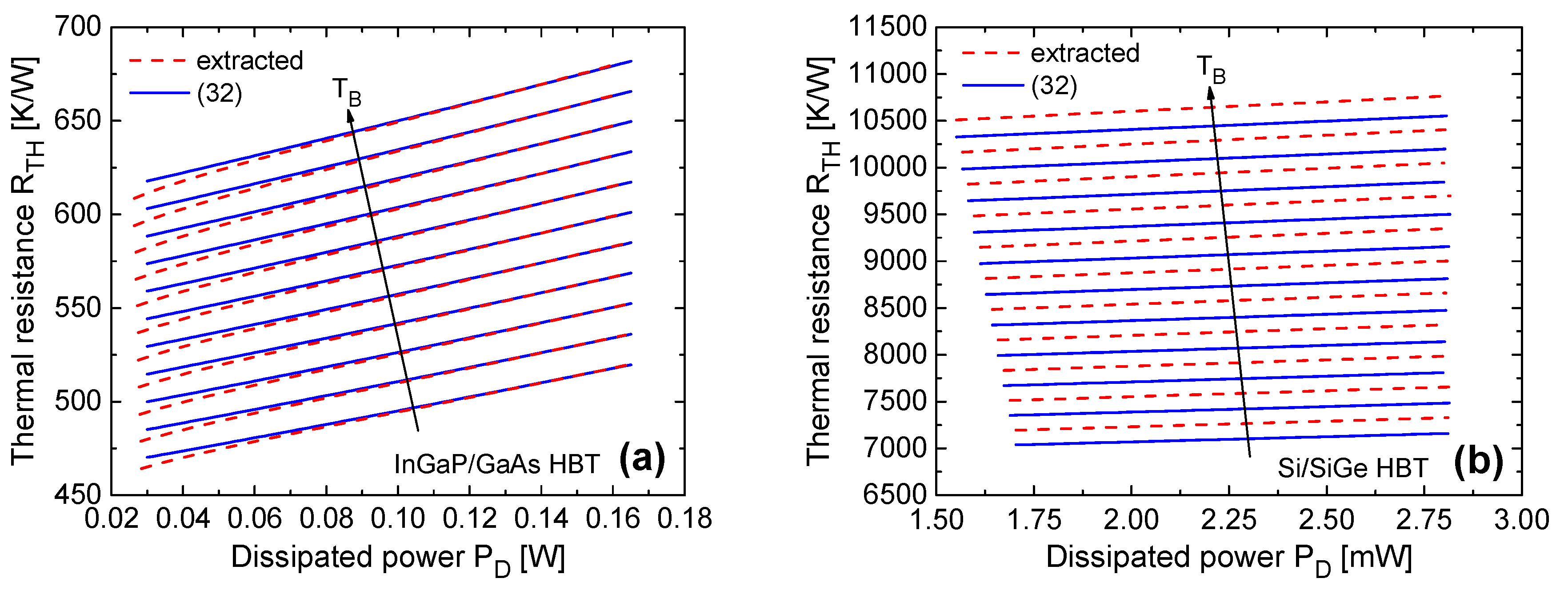
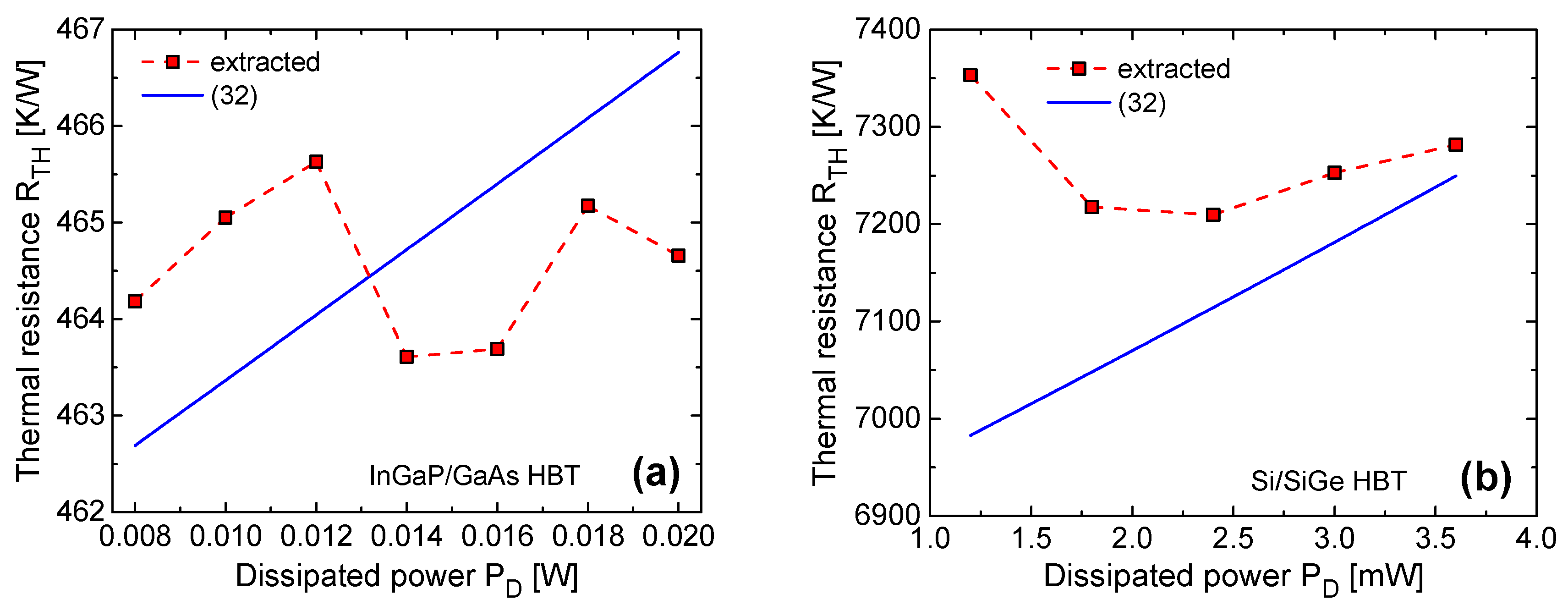
d’Alessandro et al. [18,31]The technique in [18] aims to improve the accuracy in the extraction of coefficient ϕ with respect to the approaches of Dawson et al. and Rieh et al., the price to pay being an increased elaboration effort. Consequently, in this case the compensation of errors does not take place, and this technique overestimates RTH with respect to RTH00 due to the nonlinear self-heating effect and the Early effect in the second measurement. The inaccuracy dictated by the nonlinear self-heating effect can be alleviated by limiting the PD range in which the RTH extraction is performed. The extended versions in [31] allow purifying the extraction from the Early effect, which is misinterpreted as additional self-heating. As a result, differently from all other techniques, the approaches in [31] can be adopted not only to NPN HBTs, but also to PNP HBTs and Si BJTs, where the Early effect plays a more relevant role.
Disclaimer/Publisher’s Note: The statements, opinions and data contained in all publications are solely those of the individual author(s) and contributor(s) and not of MDPI and/or the editor(s). MDPI and/or the editor(s) disclaim responsibility for any injury to people or property resulting from any ideas, methods, instructions or products referred to in the content.

