
Influence of the Metal–Semiconductor Interface Model on Power Conservation Principle in a Simulation of Bipolar Devices


Department of Semiconductor and Optoelectronic Devices, Lodz University of Technology, Al. Politechniki 10, 93-590 Lodz, Poland
*
Author to whom correspondence should be addressed.
Electronics 2021, 10(24), 3120; https://doi.org/10.3390/electronics10243120
Submission received: 30 October 2021
/
Revised: 6 December 2021
/
Accepted: 12 December 2021
/
Published: 15 December 2021
(This article belongs to the Special Issue Electrothermal Effects in Semiconductor Devices/Circuits)
Abstract
:The purpose of the study is to present a proper approach that ensures the energy conservation principle during electrothermal simulations of bipolar devices. The simulations are done using Sentaurus TCAD software from Synopsys. We focus on the drift-diffusion model that is still widely used for power device simulations. We show that without a properly designed contact(metal)–semiconductor interface, the energy conservation is not obeyed when bipolar devices are considered. This should not be accepted for power semiconductor structures, where thermal design issues are the most important. The correct model of the interface is achieved by proper doping and mesh of the contact-semiconductor region or by applying a dedicated model. The discussion is illustrated by simulation results obtained for the GaN p–n structure; additionally, Si and SiC structures are also presented. The results are also supported by a theoretical analysis of interface physics.
Keywords:
drift-diffusion; electrothermal; power conservation; metal–semiconductor interface; GaN; Si; SiC; bipolar1. Introduction
The proper design of power semiconductor devices is a real need of high-reliability electronics. Thermal management is even more demanding nowadays when electronics should be efficient, small in size, invisible, and maintenance-free. Silicon devices are still present on the market, whereas SiC and GaN devices have increased their market share [1]. Since power devices must be large to sustain high current densities, the drift-diffusion model is still appropriate for modeling the device structure. Furthermore, a suitable CAD model must correctly take into account electrothermal interactions. Within our work, we would like to focus on Synopsys Sentaurus TCAD™ software [2]. This software program is widely used for semiconductor devices simulation. Of course, it is not the only one available on the market. The other CAD tools used for complete semiconductor physics modeling are Atlas Silvaco TCAD™ [3], Comsol Multiphysics™ [4], Crosslight APSYS™ [5] and a few more tools developed by universities. However, here, we would like to focus on the most popular one. Sentaurus TCAD™ offers a vast set of physical models to analyze semiconductor structures. A user can choose from the drift-diffusion approach through the hydrodynamic model to the full-band Monte Carlo simulation of charge carrier transport. Within this work, we use the thermodynamic model [2], which is based on Wachutka’s work [6,7]. This model is an extension of the drift-diffusion approach with a rigorous treatment of heat transport and electrothermal effects present in semiconductors. However, the energy balance is most often not verified. Even in the application notes [8], where an electrothermal analysis of an insulated gate bipolar (IGBT) GaN transistor is presented, this problem is not discussed. Analyzing several other publications devoted to bipolar structures such as diodes, [9,10,11,12], IGBTs [13], Peltier modules [14], heterojunction bipolar transistors (HBTs) [15], we find that this problem is also not tackled. We do not want to judge if the reported results are fully correct, however, since there are no models details reported and it is not possible to confirm if all the results are fully validated.
Previously [16], we have presented that in the case of Si, to ensure the power conservation principle, the interface between the contact node and Si must contain a metal layer and a highly doped Si region. Here, we would like to present that a similar solution can be applied to GaN and SiC semiconductor devices. We would like to discuss two approaches that can be used to ensure the power conservation principle.
2. Semiconductor Structures
We have considered three very similar structures. The structure S0, shown in Figure 1a, represents the most popular approach to semiconductor structure modeling, where a default ohmic boundary condition is applied to the p- and n-type regions. Thus, there is no physical representation of the metal–semiconductor (MS) interface. This simplification does not allow for an investigation of the heat and electron transport in the metal layer. The structure S1, shown in Figure 1b, contains additional contact metal layers, whereas the structure S2 also has highly doped metal–semiconductor interfaces. Here, we assumed it is the Gaussian doping profile and is the distance where the doping reaches the bulk level and , are the concentration maxima. The structure S2 reflects more accurately the real structure of metal–semiconductor contact.
The value of the thermal resistance reflects the effective heat spreading achieved by the Golden DRAGON package [17]. The highly effective cooling was used to investigate the correctness of the models for a high current density regime.
3. Metal–Semiconductor Interface Basics
The metal–semiconductor interface may lead to rectifying or linear IV characteristics. The physics at the MS interface is not trivial. However, from the point of view of semiconductor devices technology, excluding those structures that benefit from the nonlinearity of MS interface, the role of the MS contact is to establish (only) electrical connection between the metal paths and semiconductor domain. Thus, linear ohmic contacts are used. Since the contact is not an active element of the semiconductor device structure, its model is mostly simplified. Here we would like to show that accurate modeling of the MS interface cannot be neglected. The typical energy diagram for an ohmic MS contact for an n-type or p-type semiconductor can be found in any handbook. The case of an n-type material is shown in Figure 2b. When the work function relation is obeyed, the ohmic contact is created. Fortunately, the linear contact can also be obtained when , if the barrier is so narrow that the tunneling enables the carrier transport, Figure 2d. This type of contact can be found in SiC and GaN devices. Depending on the barrier height and the thickness, the linear IV characteristic can be achieved due to the thermionic and/or the tunneling transport through the barrier [18].
Irrespective of the band diagram details at the MS interface, the carrier transport through the contact also leads to absorption or release of the heat, since the carriers’ thermal equilibrium energy is different on each side of the contact (Figure 3). This phenomenon is the well-known Peltier effect.
The electrothermal simulation of any semiconductor device should not be performed without an appropriate model of the MS interface. Surprisingly, the most popular model of ohmic contact is a simple boundary condition where the external potential is applied to a selected line or surface of a semiconductor. Within this boundary model, charge neutrality is assumed, and the contact boundary condition acts as a carrier sink [2]. However, this model, where no metal layer is present, does not allow the inclusion of heat transport at the interface. In [16], we have shown that this model leads to erroneous results, where the energy conservation principle is not obeyed. It becomes clear that the contact metal layer should be included to get the correct results. Here, we present two approaches that ensure energy balance during electrothermal simulations: the MSPeltierHeat model in Section 4 and the introduction of an additional doping profile in Section 5.1.
4. Metal–Semiconductor Interface Model
In Sentaurus TCAD™, one can use the MSPeltierHeat model. This model is not enabled by default. The Peltier heat for electrons and holes at the contact are calculated, as [2]:
For default fitting parameters , these equations simplify to
where , are the electron and hole current densities passing the interface, whereas and are the energy differences of electrons and holes, expressed in volts, on each side of the interface. The full MSPeltierHeat model uses the following equations to compute these energies, [2]:
where is the work function for the metal in V, , are the quasi-Fermi potentials for electrons and holes, , are the absolute thermoelectric powers, also referred as Seebeck coefficients [19], T is the lattice temperature, , are the conduction band and valence band energies, respectively, and q is the electron charge. With the default values of fitting parameters used for the thermodynamic model, , , the model is expressed as:
and are the average energies of electrons and holes, respectively, on the semiconductor side.
Sentaurus TCAD™ uses tabulated Seebeck coefficients, , , for silicon. The values are functions of the temperature and doping concentration. It is however possible to use an analytical model, where , are calculated as [2,19]:
where , are model parameters, equal to 1 by default, are the electron and hole concentrations, and are the effective density of states for electrons and holes. These analytical equations are used for SiC and GaN simulations due to missing tabulated values for these semiconductors. The calculated metal–semiconductor interface heat values and are not considered as volume heat sources and are assigned to the interface line directly.
5. Simulation Results for Si Structure
Among all the semiconductors available in Sentarus TCAD, the models for Si are the most reliable and verified in many simulations by a vast number of researchers. Thus, let us focus on the silicon structure first. The basic quantities that are used in the discussion are:
is the input electrical power, and I are voltage and current of the p–n structure. A part of the input power is transferred into heat and the other is emitted due to radiative recombination. The power that is transferred into heat is reported by Sentaurus TCAD™ as . If there was no radiative recombination, the following relation should be obeyed:
Then, an can be defined as:
If simulations are correctly performed, the must be close to 0; the input and output powers must be equal; there is no excuse for the energy conservation principle.
5.1. Energy Balance by Doping Profile Modification
In previous work [16], we have pointed out that for Si and SiC p–n diodes, the energy balance can be obtained even without the dedicated heat generation/absorption model for the MS interface. To achieve these results, the appropriate contact geometry must be ensured. It requires a proper thickness of the metal layer C, a high doping concentration near the contacts , , and a proper thickness of the highly doped region . When the parameters are chosen appropriately, the is minimized. In this paper, we have investigated this effect more deeply. First, analyzing the MS band structure (Figure 4c), it becomes clear that the correct results are achieved when the doping is high enough to shift the Fermi level into the conduction and valence bands for n- and p-type semiconductor, respectively. Thus, the MS interface is degenerated and the energy barrier, which usually appears at the MS contact, is shifted into the semiconductor, where the ThermoDynamic model correctly solves the problem. The energy balance is then achieved, which is proved in Figure 4b. For the structure without a highly doped contact region, the input and output powers are different (Figure 4a).
5.2. Energy Balance by the MSPeltierHeat Model
The problem of heat management at the MS interface can also be addressed by the MSPeltierHeat model, described previously in Section 4. The usage of this model is not vastly reported. Even in the electrothermal Sentarus TCAD Application note [8], the MSpeltierHeat model is not applied. The utilization of this model is directly reported in the work of Conrad [20], however no detailed analysis of the results is given.
For the simulations reported in our work, the default model parameters were used. The input electric power and output power , shown in Figure 5, were calculated with and without the MSPeltierHeat model.
The black lines are recalled from Figure 4 and present the characteristics obtained without the MSPeltierHeat model. For structure S1, without the highly doped region, the discrepancy is significant, and no energy balance is achieved. For structure S2, the conservation principle is obeyed and both approaches give the same results.
6. Simulation Results for SiC and GaN
Similar approaches are used to model SiC and GaN p–n diodes. For these semiconductors, the nickel contact is assumed to have the work function , [21].
The difference in power characteristics between SiC and GaN for the S1 structure (Figure 6a,c) is caused by the opposite type of electrothermal feedback resulting from a different set of material parameters, energy band gap model, mobility model, and thermoelectric models.
The results, shown in Figure 6 confirm that the results are correct when the MSPeltierHeat model is used, or the additional high doping profile is added in the vicinity of the metal–semiconductor interface.
It must be emphasized that the electrical power is equal to the dissipated heat only when the radiative recombination is not present. Such an assumption is justified for SiC. However, the radiative recombination cannot be neglected for GaN structures. Of course, the light is not emitted outside of the GaN power devices, but the internal energy transport is affected by this process. Being sure of the correctness of the thermodynamic solution, one can also predict the amount of energy involved in the radiative recombination process by investigating the difference between input power and dissipated heat. The results for GaN with radiative recombination model are shown in Figure 7.
7. Influence of the Doping Profile on ErrorP
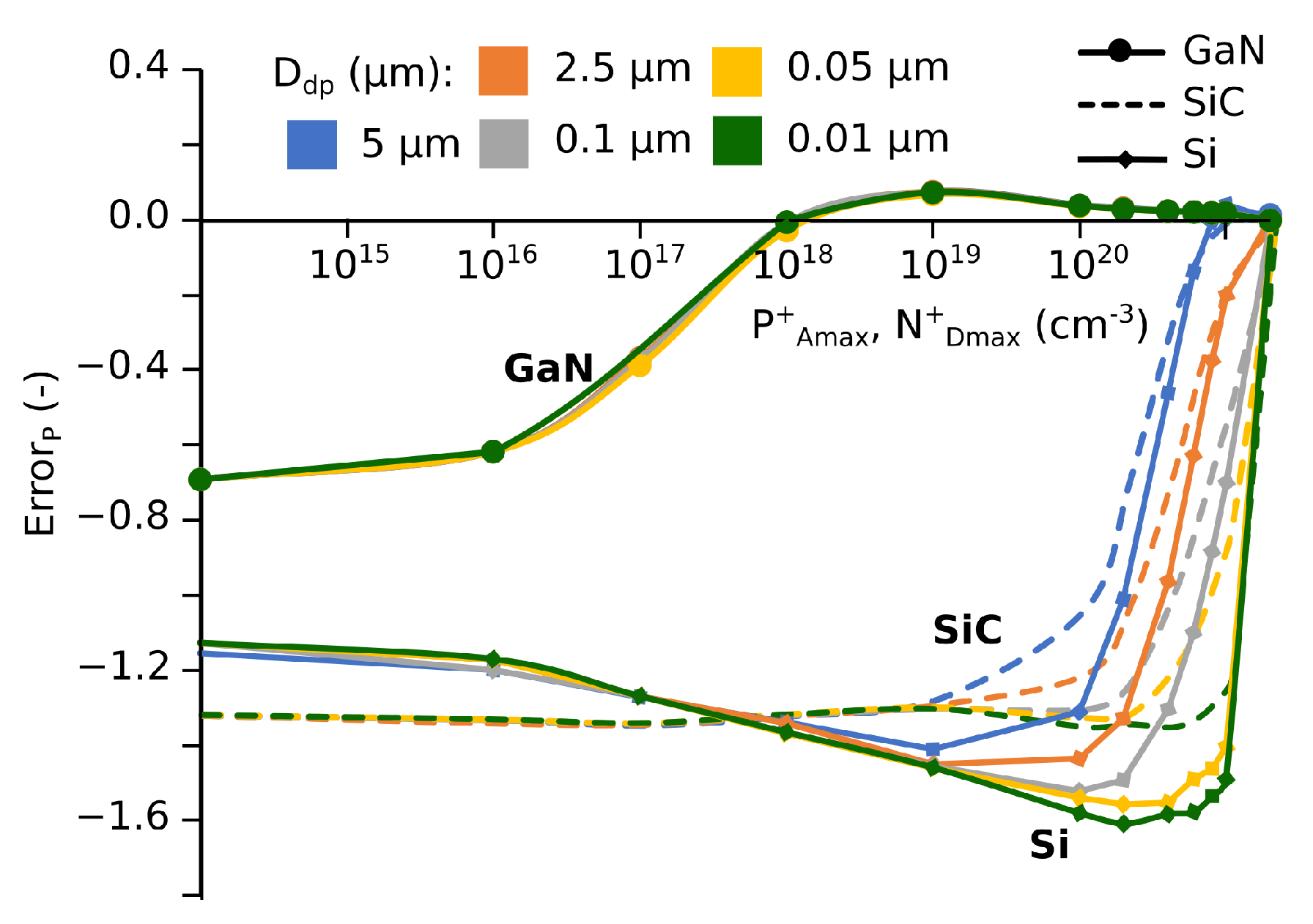
The results obtained for all three semiconductors confirm that when the doping in the vicinity of the contact is high enough, the energy balance can be retrieved. The question is what the doping level should be. To answer this question, let us plot as a function of doping concentration peak for different thickness of the profile . To make the comparison possible, is calculated when the current density reaches .
The results depicted in Figure 8 show that the region near the MS interface must be a degenerate semiconductor with a doping concentration reaching –. The doping may be lowered when the thickness of the highly doped region is increased. Since the modification of the metal–semiconductor interface should not affect the geometry of the structure, should be as small as possible.
8. Summary
It was shown that the Sentarus TCAD electrothermal simulation of bipolar structures requires an interface that consists of a metal layer and a highly doped semiconductor region. If the standard ohmic boundary condition is applied, the dissipated power is strongly underestimated. The energy balance can be achieved if the MSPeltierHeat model is utilized, or a degenerate semiconductor region is introduced. The power balance must always be checked when the second method is used since not every doping profile leads to expected results. The MSPeltierHeat method calculates the heat gain/loss directly at the interface. In contrast, the introduction of the doped layer shifts the MS interface phenomena into the semiconductor, where the Thermodynamic model copes with it.
Author Contributions
Conceptualization, J.W.; methodology, J.W.; validation, J.W., formal analysis, J.W.; investigation, J.W. and Z.L.; resources, J.P.; writing—original draft preparation, J.W.; writing—review and editing, J.W. and J.P.; visualization, J.W. and J.P.; supervision, Z.L.; project administration, Z.L.; funding acquisition, Z.L. All authors have read and agreed to the published version of the manuscript.
Funding
This research received no external funding.
Data Availability Statement
The data presented in this study are available on request from the corresponding author.
Conflicts of Interest
The authors declare no conflict of interest.
Abbreviations
The following abbreviations are used in this manuscript:
| IGBT | insulated gate bipolar transistor |
| HBT | heterojunction bipolar transistor |
| MS | metal–semiconductor |
References
- Zojer, B. Driving 600 V CoolGaN(TM) High Electron Mobility Transistors; Infineon Technologies AG: Munich, Germany, 2018. [Google Scholar]
- Sentaurus. Sentaurus(TM) Device User Guide; Synopsys, Inc.: Mountain View, CA, USA, 2021; Available online: https://www.synopsys.com/search.html#q=Sentaurus(TM)%20Device%20User%20Guide&t=All&sort=relevancy (accessed on 2 December 2021).
- Silvaco. Device Simulation Software; Version 5.20. 2; ATLAS User’s Manual; Silvaco: Santa Clara, CA, USA, 2015; Available online: https://silvaco.com (accessed on 2 December 2021).
- COMSOL. COMSOL Multiphysics; v. 5.6; COMSOL AB: Stockholm, Sweden; Available online: https://www.comsol.com (accessed on 3 December 2021).
- Crosslight Software. APSYS by Crosslight Software, Inc.; Crosslight Software: Burnaby, BC, Canada; Available online: http://crosslight.com (accessed on 3 December 2021).
- Wachutka, G.K. Rigorous thermodynamic treatment of heat generation and conduction in semiconductor device modeling. IEEE Trans. Comput.-Aided Des. Integr. Circuits Syst. 1990, 9, 1141–1149. [Google Scholar] [CrossRef] [Green Version]
- Wolbert, P.B.; Wachutka, G.K.; Krabbenborg, B.H.; Mouthaan, T.J. Nonisothermal device simulation using the 2D numerical process/device simulator TRENDY and application to SOI-devices. IEEE Trans. Comput.-Aided Des. Integr. Circuits Syst. 1994, 13, 293–302. [Google Scholar] [CrossRef]
- Sentaurus. Sentaurus Technology Template: IGBT Characterization; Synopsys, Inc.: Mountain View, CA, USA, 2021; Available online: https://www.synopsys.com/search.html#q=Sentaurus%20Technology%20Template%3A%20IGBT%20Characterization&t=All&sort=relevancy (accessed on 2 December 2021).
- Pavelek, M.; Frivaldsky, M.; Sojka, P.; Morgos, J. Electro-Thermal Modelling and Experimental Verification of Power Semiconductor Diode. Elektronika ir Elektrotechnika 2020, 26, 48–53. [Google Scholar] [CrossRef]
- Kaïd, A.; Roqueta, F.; Kammerer, J.B.; Hébrard, L. Electro-thermal Modeling Method of Protection Power Diodes Using TCAD 3D/2D approach. In Proceedings of the 2019 25th International Workshop on Thermal Investigations of ICs and Systems (THERMINIC), Lecco, Italy, 25–27 September 2019; pp. 1–6. [Google Scholar]
- Fichtner, S.; Lutz, J.; Basler, T.; Rupp, R.; Gerlach, R. Electro-thermal simulations and experimental results on the surge current capability of 1200 V SiC MPS diodes. In CIPS 2014, Proceedings of the 8th International Conference on Integrated Power Electronics Systems, Nuremberg, Germany, 25–27 February 2014; VDE: Frankfurt, Germany, 2014; pp. 1–6. [Google Scholar]
- Wang, A.; Bai, Y.; Tang, Y.; Li, C.; Han, Z.; Lu, J.; Chen, H.; Tian, X.; Yang, C.; Hao, J.; et al. Analysis of Transient Surge Current Mechanism in SiC MPS Diode With the Transition Region. IEEE Trans. Electron Devices 2021, 68, 6330–6337. [Google Scholar] [CrossRef]
- Jin, R.; Wang, Y.; Li, L.; Xu, L.; Pu, K.; Zeng, J.; Darwish, M. Comparative study of electro-thermal characteristics of 4500 V diffusion-CS IGBT and buried-CS IGBT. IET Circuits Devices Syst. 2021, 15, 251–259. [Google Scholar] [CrossRef]
- Gould, C.; Shammas, N. Three dimensional TCAD simulation of a thermoelectric module suitable for use in a thermoelectric energy harvesting system. Small-Scale Energy Harvest. 2012, 29. [Google Scholar] [CrossRef] [Green Version]
- Petrosyants, K.; Torgovnikov, R. Electro-thermal modeling of trench-isolated SiGe HBTs using TCAD. In Proceedings of the 2015 31st Thermal Measurement, Modeling & Management Symposium (SEMI-THERM), San Jose, CA, USA, 15–19 March 2015; pp. 172–175. [Google Scholar]
- Wozny, J.; Podgorski, J.; Raj, E.; Lisik, Z. Good Practices of Electrothermal Simulation of pn Structures Using Sentaurus TCAD. In Proceedings of the IEEE 15th International Conference on the Experience of Designing and Application of CAD Systems (CADSM), Polyana, Ukraine, 26 February–2 March 2019; p. 1. [Google Scholar]
- OSRAM. Golden DRAGON Datasheet; OSRAM Opto Semiconductors GmbH: Regensburg, Germany, 2017; Available online: https://www.osram.com (accessed on 1 June 2019).
- Latreche, A. Combination of thermionic emission and tunneling mechanisms to analyze the leakage current in 4H-SiC Schottky barrier diodes. Semicond. Phys. Quantum Electron. Optoelectron. 2019, 22, 19–25. [Google Scholar] [CrossRef] [Green Version]
- Velmre, E.; Udal, A. Modelling of Charge Carrier Nonisothermal Transport in Silicon and Silicon Carbide. Proc. Estonian Acad. Sci. Eng. 2000, 6, 144–154. [Google Scholar]
- Conrad, K. A Physics-Based Compact Model for Thermoelectric Devices. Ph.D. Thesis, Purdue University, West Lafayette, IN, USA, 2015. [Google Scholar]
- Ofuonye, B.; Lee, J.; Yan, M.; Sun, C.; Zuo, J.M.; Adesida, I. Electrical and microstructural properties of thermally annealed Ni/Au and Ni/Pt/Au Schottky contacts on AlGaN/GaN heterostructures. Semicond. Sci. Technol. 2014, 29, 095005. [Google Scholar] [CrossRef]
Figure 1.
Different structures that can be used to model p–n junction. (a) Structure S0, default ohmic boundary condition. (b) Structure S1, metal contact. (c) Structure S2, metal-highly doped regions close to the contacts, m, m.
Figure 1.
Different structures that can be used to model p–n junction. (a) Structure S0, default ohmic boundary condition. (b) Structure S1, metal contact. (c) Structure S2, metal-highly doped regions close to the contacts, m, m.

Figure 2.
(a) Energy band diagram before contact for . (b) Classic ohmic contact. (c) Energy band diagram before contact for . (d) Tunneling ohmic contact.
Figure 2.
(a) Energy band diagram before contact for . (b) Classic ohmic contact. (c) Energy band diagram before contact for . (d) Tunneling ohmic contact.
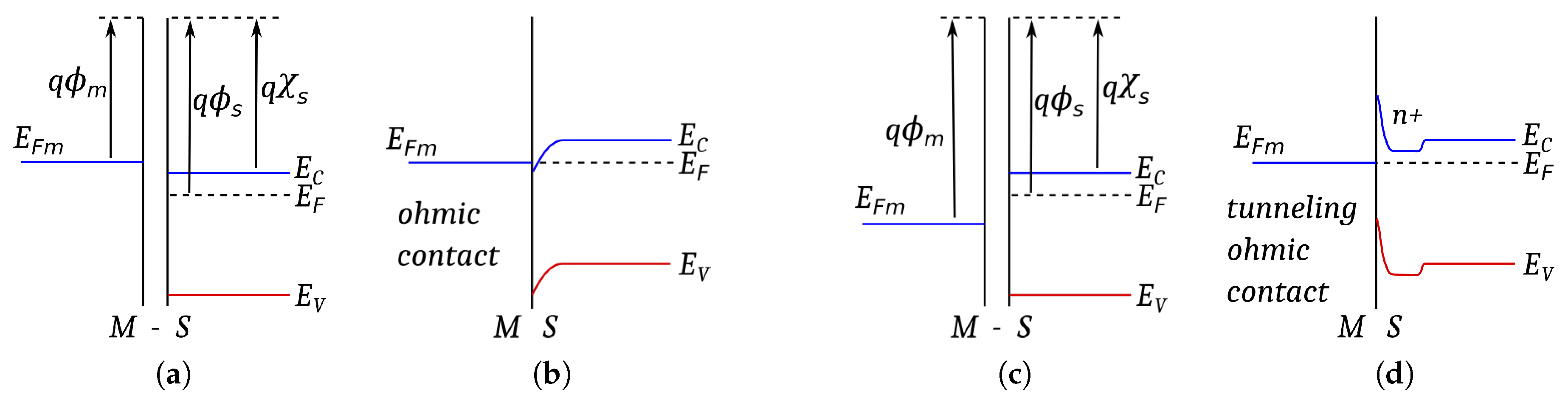
Figure 3.
(a) Heat absorption by electrons at MS interface. (b) Heat release at MS interface.
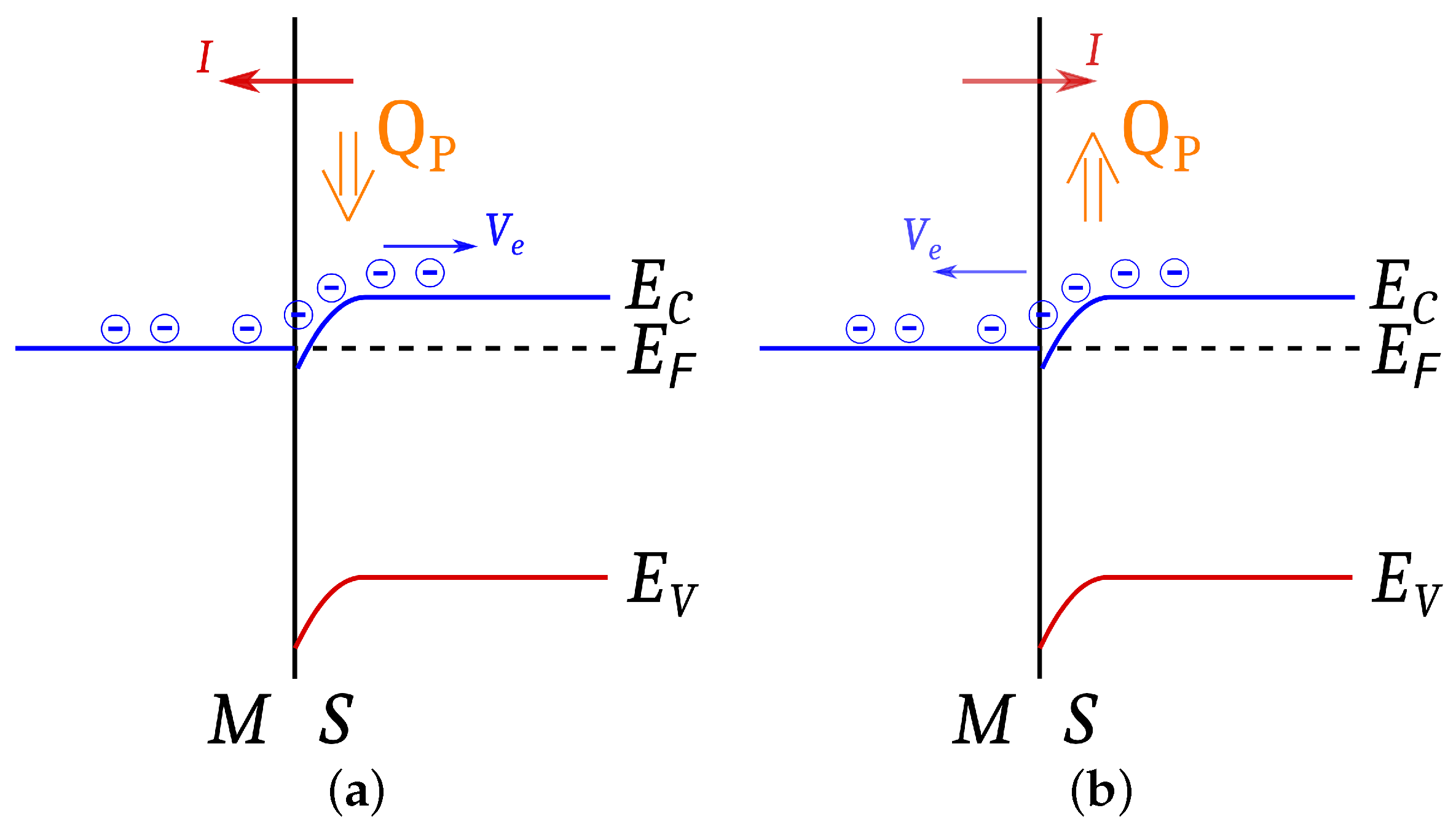
Figure 4.
Power balance and the energy band diagrams for Si structures S1 and S2; geometry parameters are: m, , m. (a) Input and output powers for S1; (b) input and output powers for S2; (c) energy band diagrams for S1 and S2.
Figure 4.
Power balance and the energy band diagrams for Si structures S1 and S2; geometry parameters are: m, , m. (a) Input and output powers for S1; (b) input and output powers for S2; (c) energy band diagrams for S1 and S2.
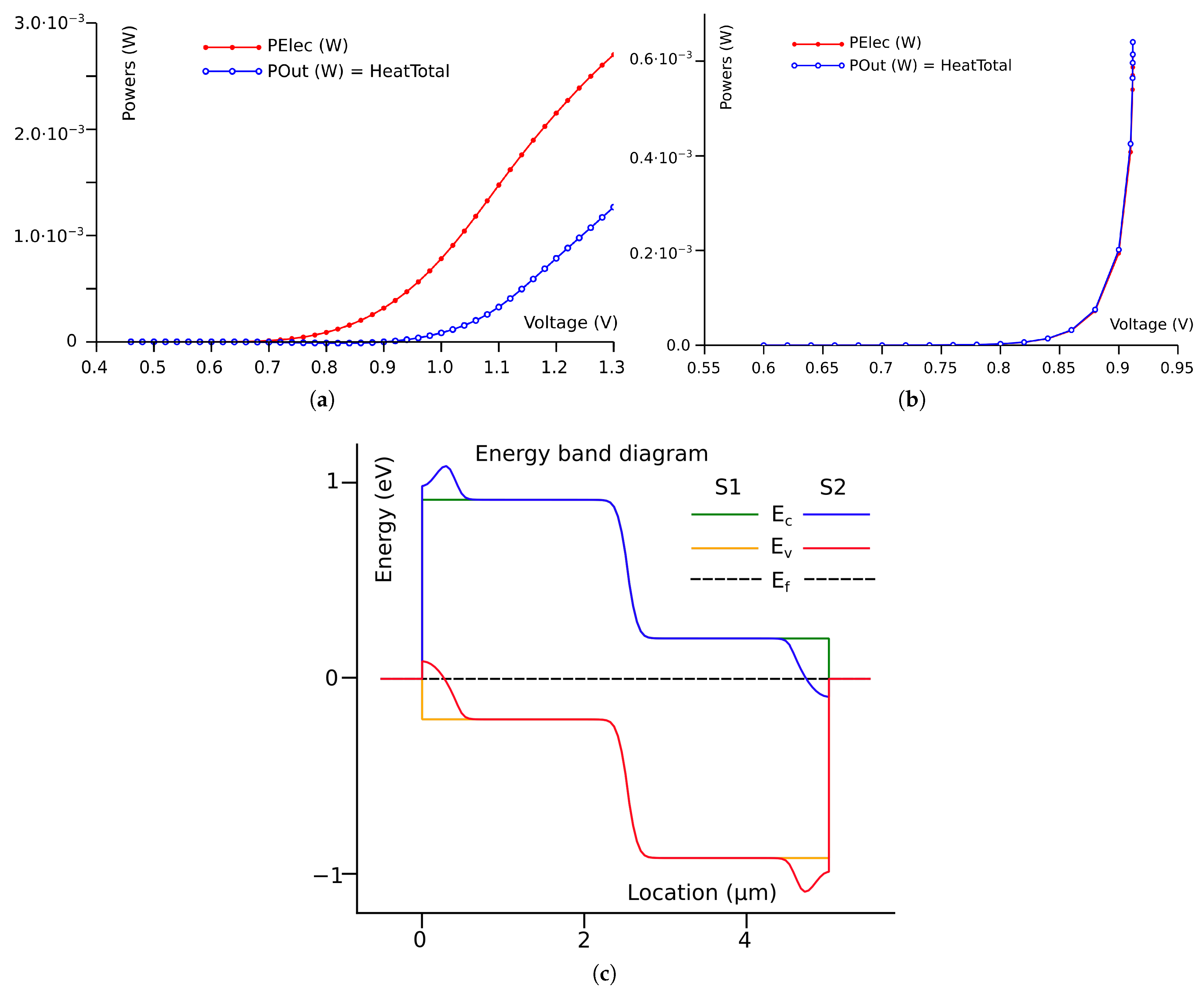
Figure 5.
Powers calculated with and without the MSPeltierHeat model for (a) geometry S1, (b) geometry S2. The structure parameters were m, , m.
Figure 5.
Powers calculated with and without the MSPeltierHeat model for (a) geometry S1, (b) geometry S2. The structure parameters were m, , m.

Figure 6.
Input and output powers for SiC and GaN, structures S1 and S2, the structure parameters are: m, , m, radiative recombination model is off. (a) SiC, S1; (b) SiC, S2; (c) GaN, S1; (d) GaN, S2.
Figure 6.
Input and output powers for SiC and GaN, structures S1 and S2, the structure parameters are: m, , m, radiative recombination model is off. (a) SiC, S1; (b) SiC, S2; (c) GaN, S1; (d) GaN, S2.

Figure 7.
Input and output powers for GaN with radiative recombination model, for structures S1 and S2; structure parameters are: m, , m; (a) GaN, S1; (b) GaN, S2.
Figure 7.
Input and output powers for GaN with radiative recombination model, for structures S1 and S2; structure parameters are: m, , m; (a) GaN, S1; (b) GaN, S2.
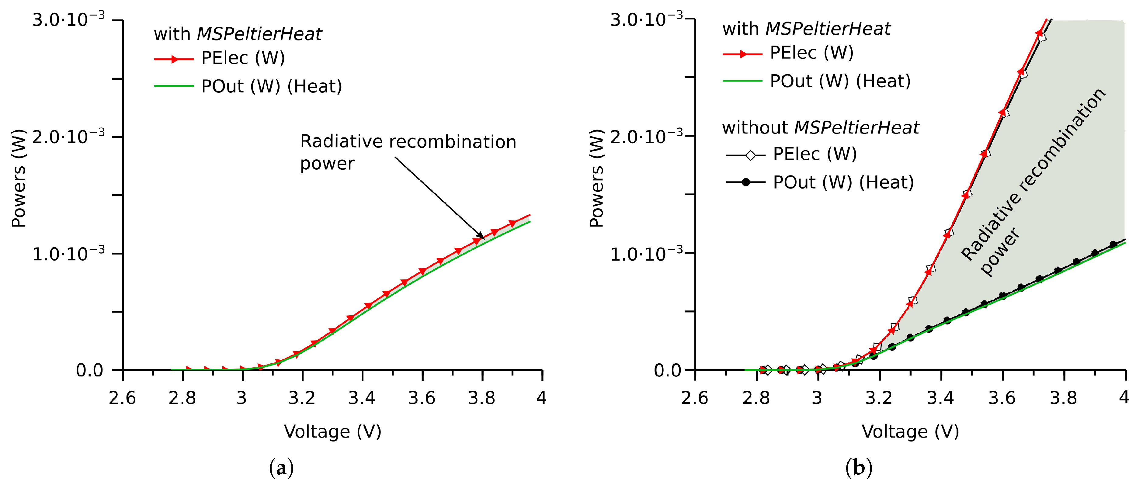
Figure 8.
as the function of doping maxima for different thickness of the profile .
Publisher’s Note: MDPI stays neutral with regard to jurisdictional claims in published maps and institutional affiliations. |
© 2021 by the authors. Licensee MDPI, Basel, Switzerland. This article is an open access article distributed under the terms and conditions of the Creative Commons Attribution (CC BY) license (https://creativecommons.org/licenses/by/4.0/).
Share and Cite
MDPI and ACS Style
Wozny, J.; Lisik, Z.; Podgorski, J. Influence of the Metal–Semiconductor Interface Model on Power Conservation Principle in a Simulation of Bipolar Devices. Electronics 2021, 10, 3120. https://doi.org/10.3390/electronics10243120
AMA Style
Wozny J, Lisik Z, Podgorski J. Influence of the Metal–Semiconductor Interface Model on Power Conservation Principle in a Simulation of Bipolar Devices. Electronics. 2021; 10(24):3120. https://doi.org/10.3390/electronics10243120
Chicago/Turabian StyleWozny, Janusz, Zbigniew Lisik, and Jacek Podgorski. 2021. "Influence of the Metal–Semiconductor Interface Model on Power Conservation Principle in a Simulation of Bipolar Devices" Electronics 10, no. 24: 3120. https://doi.org/10.3390/electronics10243120
Note that from the first issue of 2016, this journal uses article numbers instead of page numbers. See further details here.