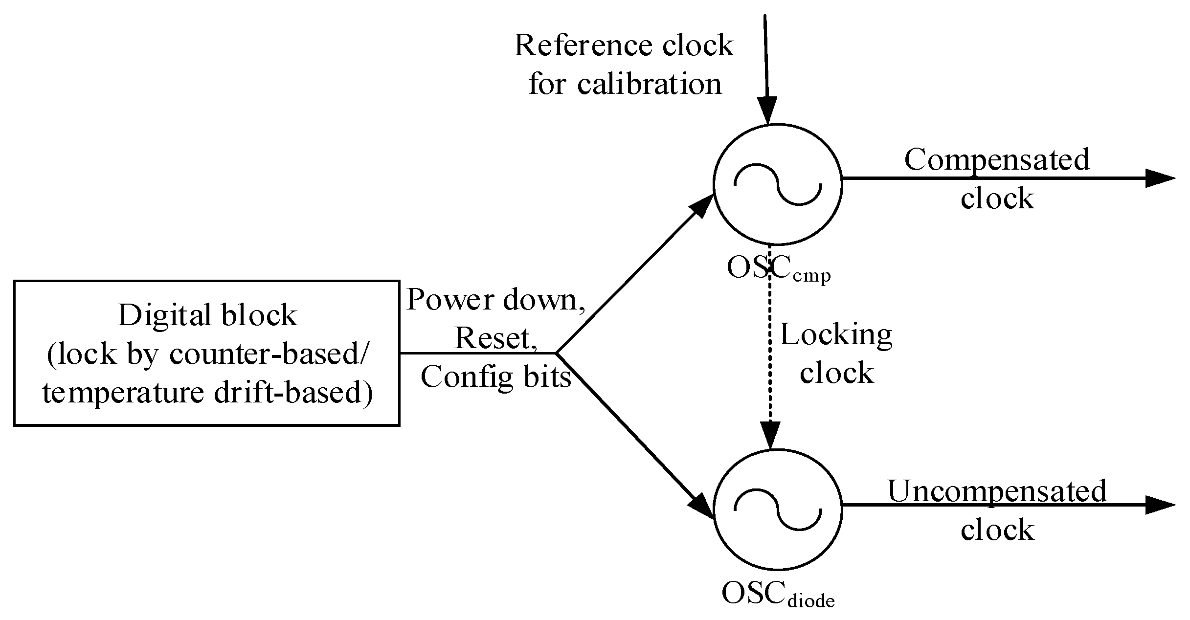
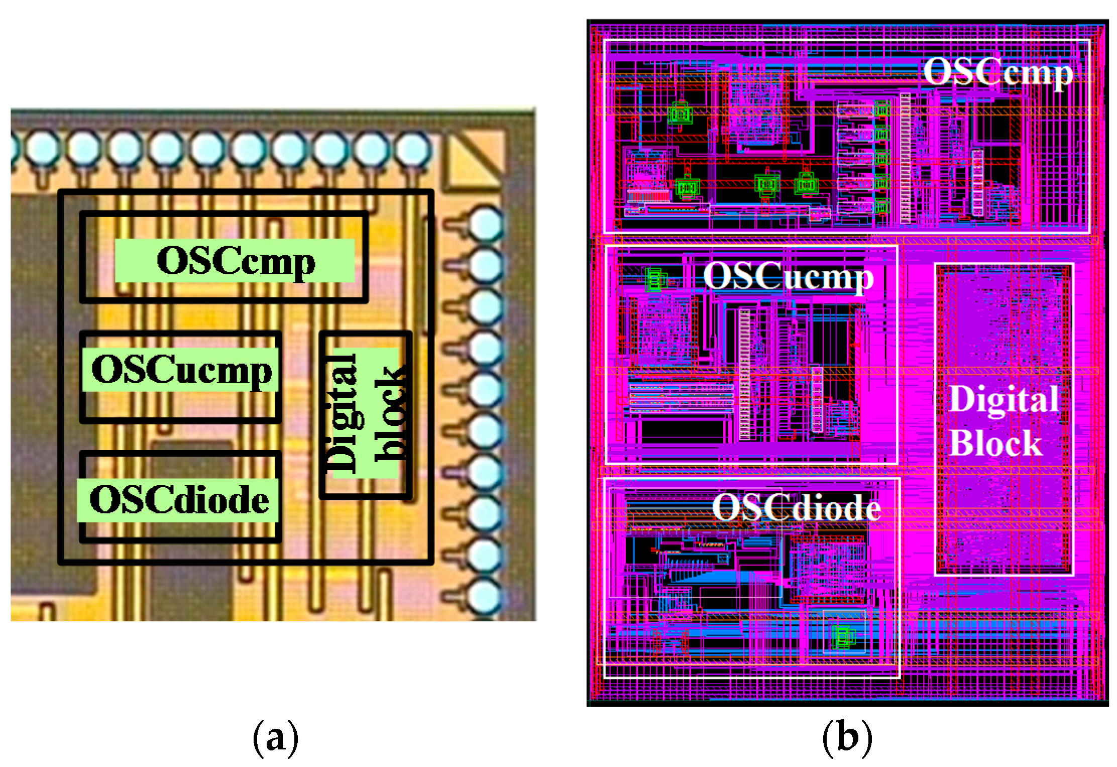
In this paper, we demonstrate a fully integrated clock source system as shown in
Figure 1. The system consists of a high stability temperature-compensated digitally controlled oscillator (DCO) implemented in [
12] (OSC
cmp), a low-power temperature-uncompensated, diode-connected-transistor-based ULP DCO (OSC
diode) that is capable of being frequency locked to OSC
cmp and acts as the system clock, and a digital block that can perform locking using a counter-based scheme implemented on-chip or a temperature-drift prediction-based mode that was verified off-chip. OSC
diode consumes lower power than the uncompensated DCO implemented in [
12] (OSC
ucmp, which uses the leakage current of “off” low-threshold (LVT) transistors as the current source). OSC
diode also has improved temperature and voltage stability over OSC
ucmp. When OSC
diode is locked to OSC
cmp often enough to compensate for the drift in the unstable clock, the clock stability of OSC
diode is within the stability bound of OSC
cmp. We demonstrate the locking function in two different modes (counter-based locking and temperature drift-based locking), eliminating the need for high power PLLs. In this section, we describe the components and design techniques used in this clock source system.
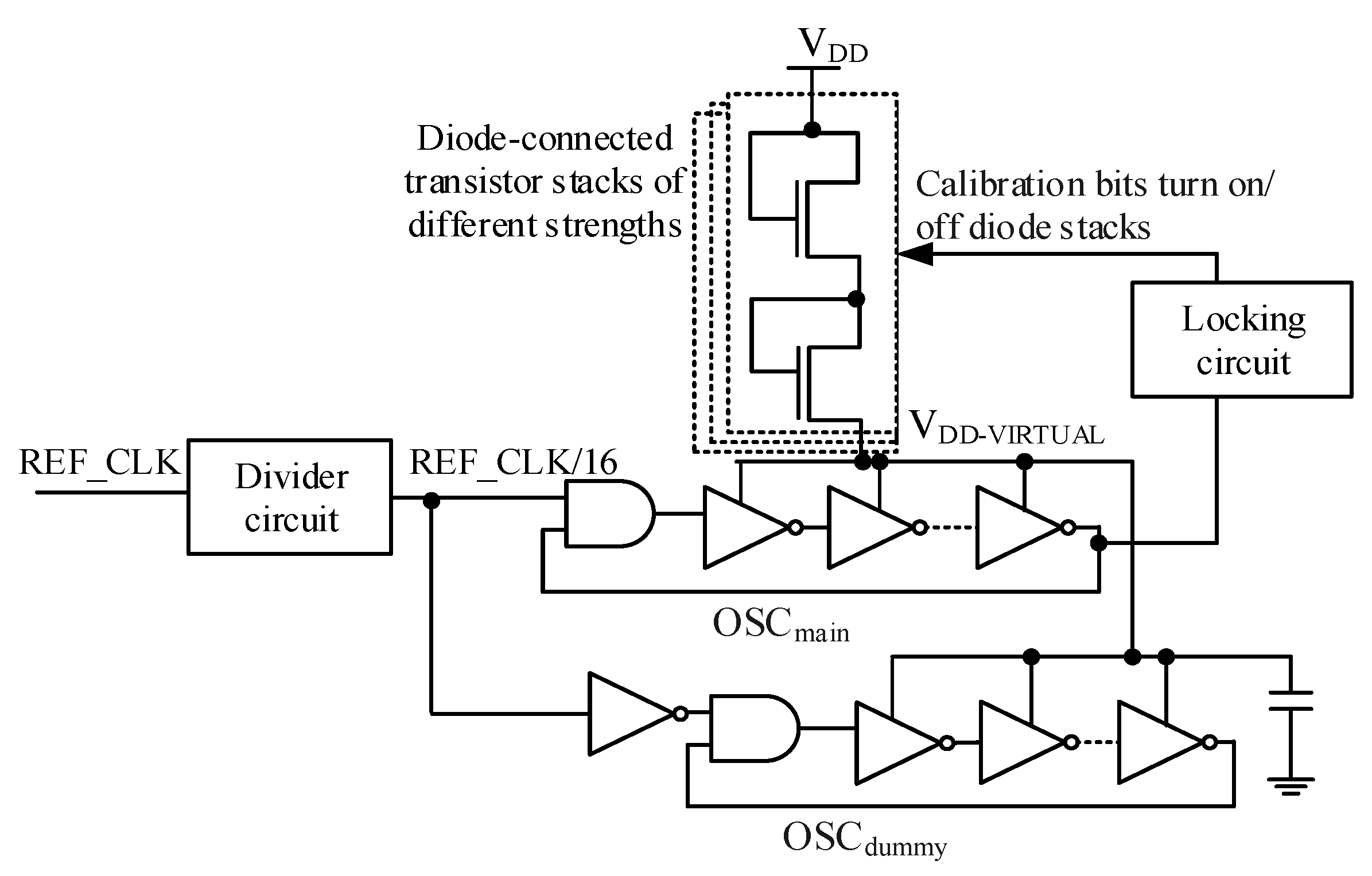
2.1. Temperature-Uncompensated Diode-Connected-Transistor Oscillator (OSCdiode)
In this paper, we propose an ULP temperature-uncompensated oscillator, the diode-connected transistor-based DCO, OSC
diode. Diode-connected MOS devices are used to generate a virtual power rail (V
DD-VIRTUAL) from the oscillator power-supply (V
DD). The oscillator is powered by V
DD-VIRTUAL as shown in
Figure 3. In this subsection, we will describe the design and oscillator stabilization techniques used in OSC
diode.
The diode strength is a function of the width of the diode transistor. Diode-connected transistor stacks sized in a binary-weighted fashion are turned on/off by a 23-bit control signal. This controls the value of VDD-VIRTUAL to obtain different frequencies. For a higher 23-bit value, VDD-VIRTUAL increases and hence raises the oscillation frequency. Thus, setting the 23 calibration bits tunes the oscillator to a specific frequency.
The stacked OSC
diode transistors have
VGS (gate-to-source voltage) equal to
VDS (drain-to-source voltage). However,
VGS (=
VDS) is less than
VT (threshold voltage). Therefore, the transistors operate in the sub-threshold region. The drain current in the sub-threshold region is given by:
µ
o is the carrier mobility, C
ox is the gate oxide capacitance, W and L are the channel width and length, and n is the sub-V
T slope factor. In the diode-connected transistors,
VDS > 3φ
t and Equation (1) can be approximated as:
This is the sub-VT MOSFET saturation region, in which the drain current becomes independent of VDS. A detailed analysis of the temperature coefficient (TC) of the different factors such as threshold voltage and carrier mobility with temperature is out of the scope of this paper. However, relevant equations to explain the temperature dependence are presented below.
The temperature dependence of the threshold voltage and the mobility is typically modeled as:
V
T0 is the threshold voltage at 0 K, and κ is the TC of V
T, T is the target temperature [
13].
μ(T
0) is the carrier mobility at room temperature T
0, m is the mobility temperature exponent [
13].
The sub-threshold current TC can be derived as follows [
14]:
From the above equation, we observe that as V
GS is lower (as transistor goes into weaker inversion), the TC increases. In diode-connected transistors in OSC
diode, V
GS = V
DS and in the uncompensated oscillator OSC
ucmp in [
12], V
GS = 0. Therefore, transistors in OSC
ucmp are in a weaker inversion than the transistors in OSC
diode and TC for diode-connected transistors is lower. However, a completely direct comparison is not possible because the current source in OSC
ucmp [
12] is the leakage current of “off” LVT transistors. The temperature dependence of V
T also determines the effective TC for both the DCOs. The TC for LVT devices is lower than high V
T devices, which is favorable for OSC
ucmp in [
12]. However, during design, we observed that a higher V
GS has a stronger effect on lowering the TC than a lower V
T. We verify this with the TC measurement of the DCOs toward the end of this section to conclude that OSC
diode has a lower TC than OSC
ucmp.
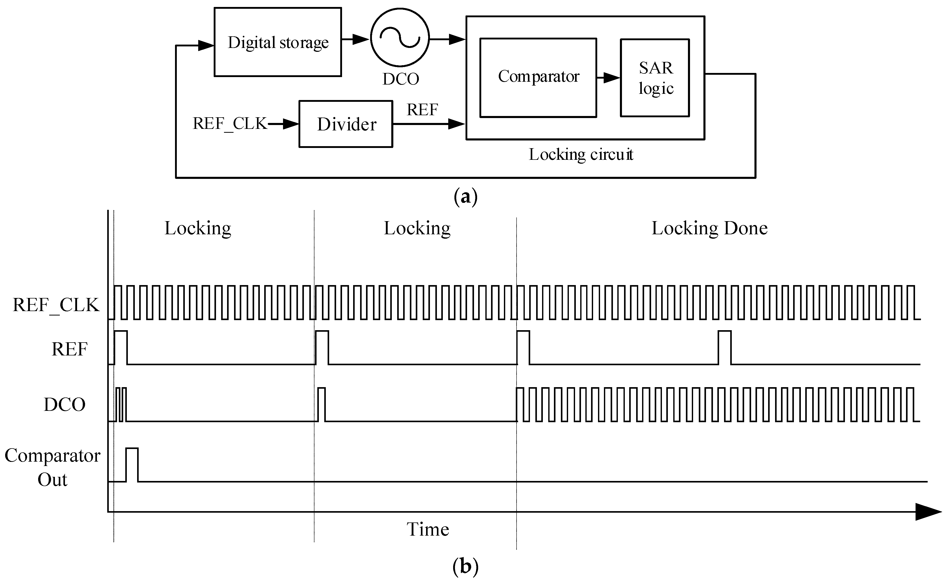
OSC
diode uses the DCO architecture shown in
Figure 4a [
12] that comprises an oscillator, a locking circuit, and digital storage for the 23 calibration bits. OSC
diode can lock to the frequency of a reference clock (REF_CLK), which in this system is the temperature-compensated oscillator OSC
cmp. The REF_CLK is divided by 16 to obtain REF. During locking, OSC
diode (DCO) is enabled when REF goes “high” (calibration time). The locking circuit consists of a frequency comparator and a successive approximation register (SAR) logic. The frequency comparator, which is implemented using a 5-bit counter, compares the frequency of OSC
diode and REF. It counts the number of OSC
diode cycles when REF is high. As shown in
Figure 4b, the output of the comparator is “1” when the count is greater than 1, and “0” otherwise. When REF is low (settling time), the SAR logic sets the 23 configuration bits of the OSC
diode one after the other in the digital storage registers, depending on the output of the comparator (1 or 0). It takes 23 locking cycles to set all the calibration bits, however only two such cycles are shown in
Figure 4b. Once all the SAR configuration bits are set and locking is done, the OSC
diode will be frequency locked to REF_CLK as shown in
Figure 4b.
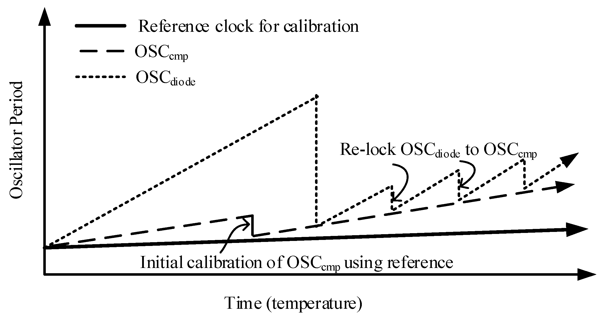
During locking, the instantaneous frequency of OSCdiode is affected. Therefore, the re-locking can take place during the idle times of the sensor operation. The chip can also be designed to send an interrupt that halts its execution while calibrating the clock.
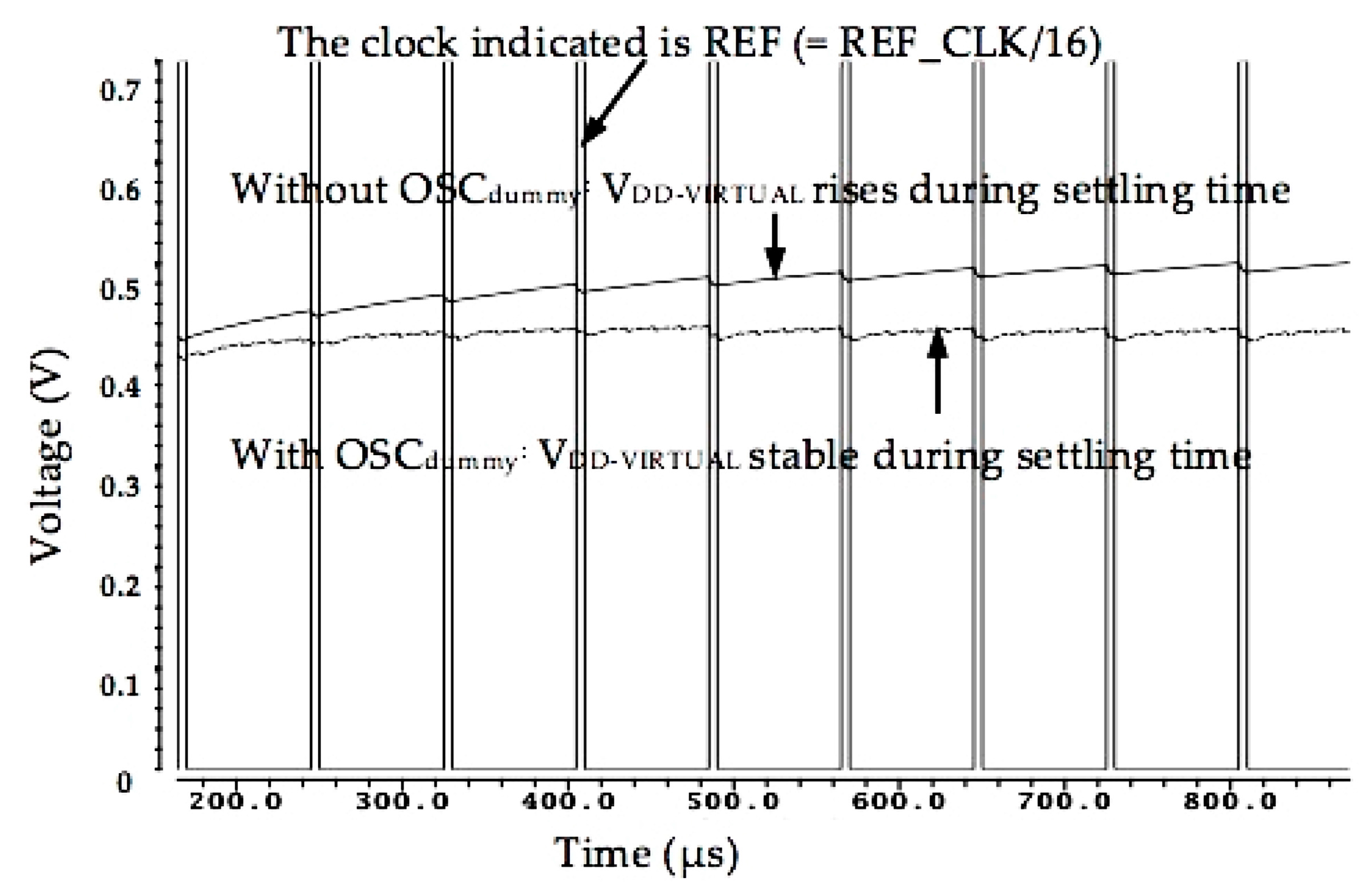
Two techniques are used to stabilize OSC
diode. First, OSC
diode requires sufficient time to stabilize after a change in the SAR bits. This is achieved by dividing REF_CLK by 16 (REF=REF_CLK/16) and allocating 1/16 of the REF period (1 REF_CLK cycle) for comparison and the other 15/16 of the REF period (15 REF_CLK cycles) to settle V
DD-VIRTUAL. V
DD-VIRTUAL takes more time to settle because of the diode charging it. Dividing REF_CLK by a number lower than 16 (such as dividing by 2 in OSC
ucmp [
12], by 4 or by 8) results in insufficient time to stabilize it. This gives a longer time (15 REF_CLK cycles) for the V
DD-VIRTUAL rail to settle before the next comparison process sets the next SAR bit.
Secondly, OSC
diode includes both a primary oscillator (OSC
main) and a dummy oscillator (OSC
dummy), with the clock output derived from OSC
main. OSC
dummy improves the load mismatch on the V
DD-VIRTUAL rail. When REF is high, OSC
main is enabled and consumes a specific amount of current. During its low state, OSC
main does not oscillate, and its current consumption reduces, causing V
DD-VIRTUAL to increase as shown in
Figure 5. This causes OSC
diode to finally settle at the wrong frequency. As a remedy, OSC
dummy is enabled when OSC
main is disabled and
vice-versa, which helps to maintain a roughly constant current draw from V
DD-VIRTUAL in both high and low states of REF. This enables OSC
main to settle at the right frequency. A simulation of the above stabilization techniques is shown in
Figure 5.
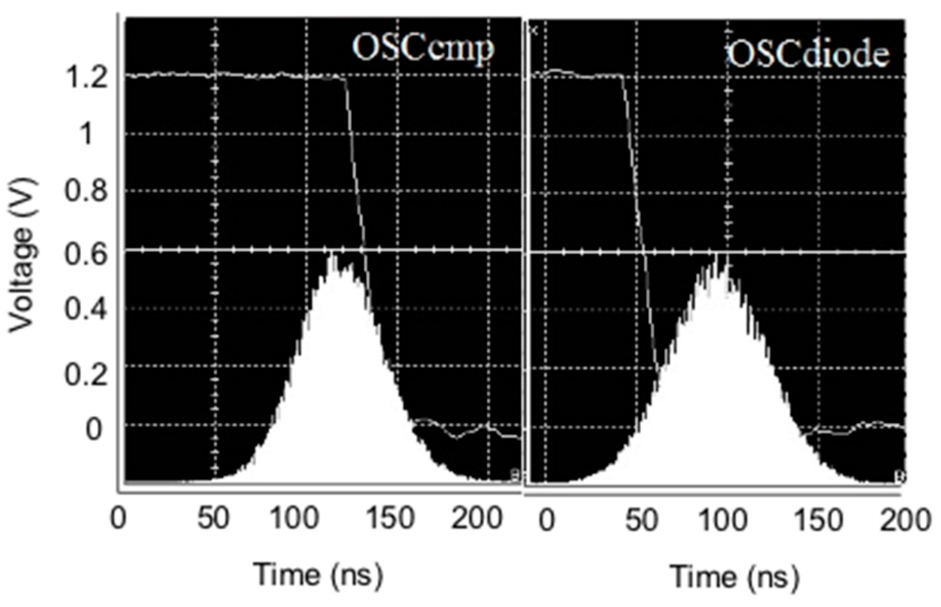
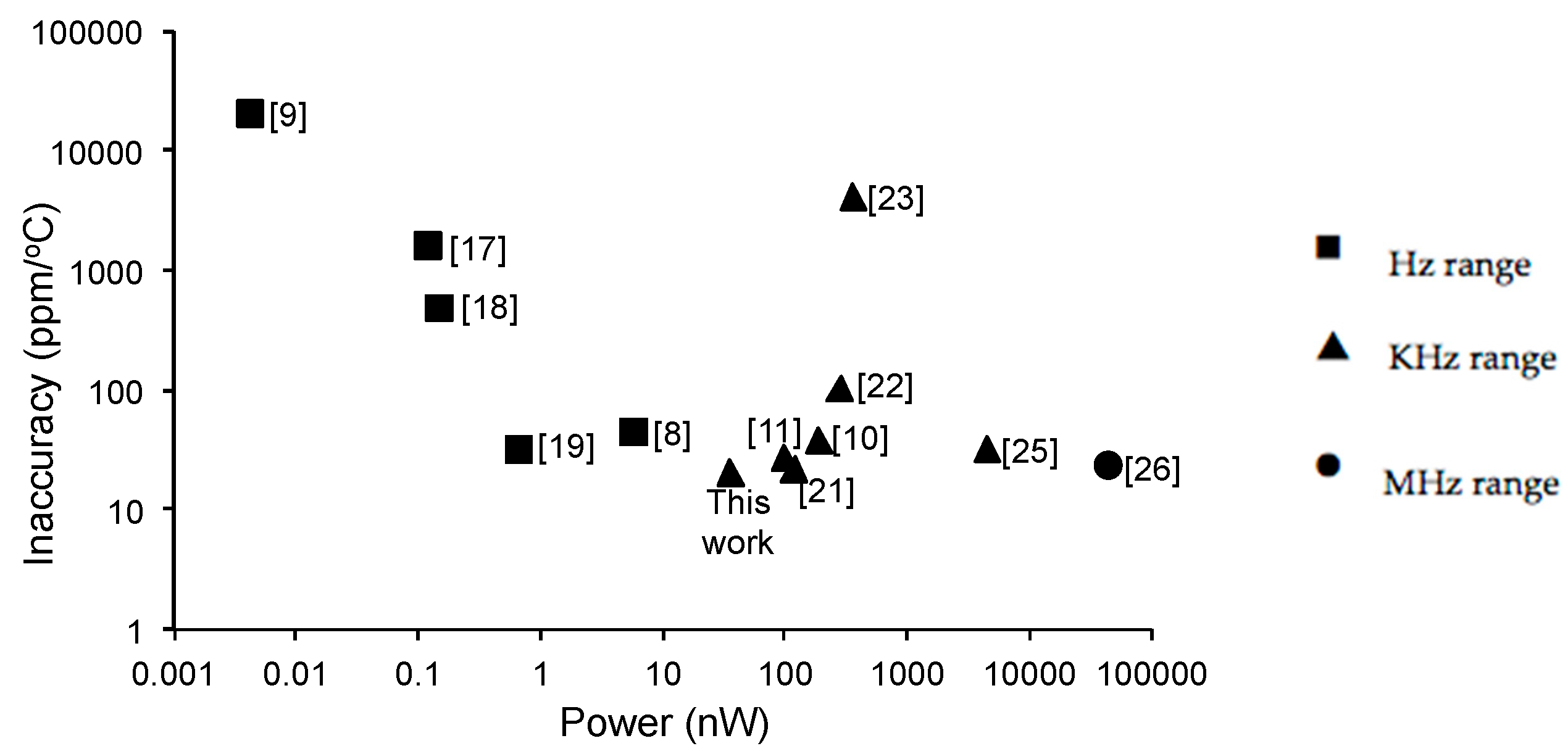
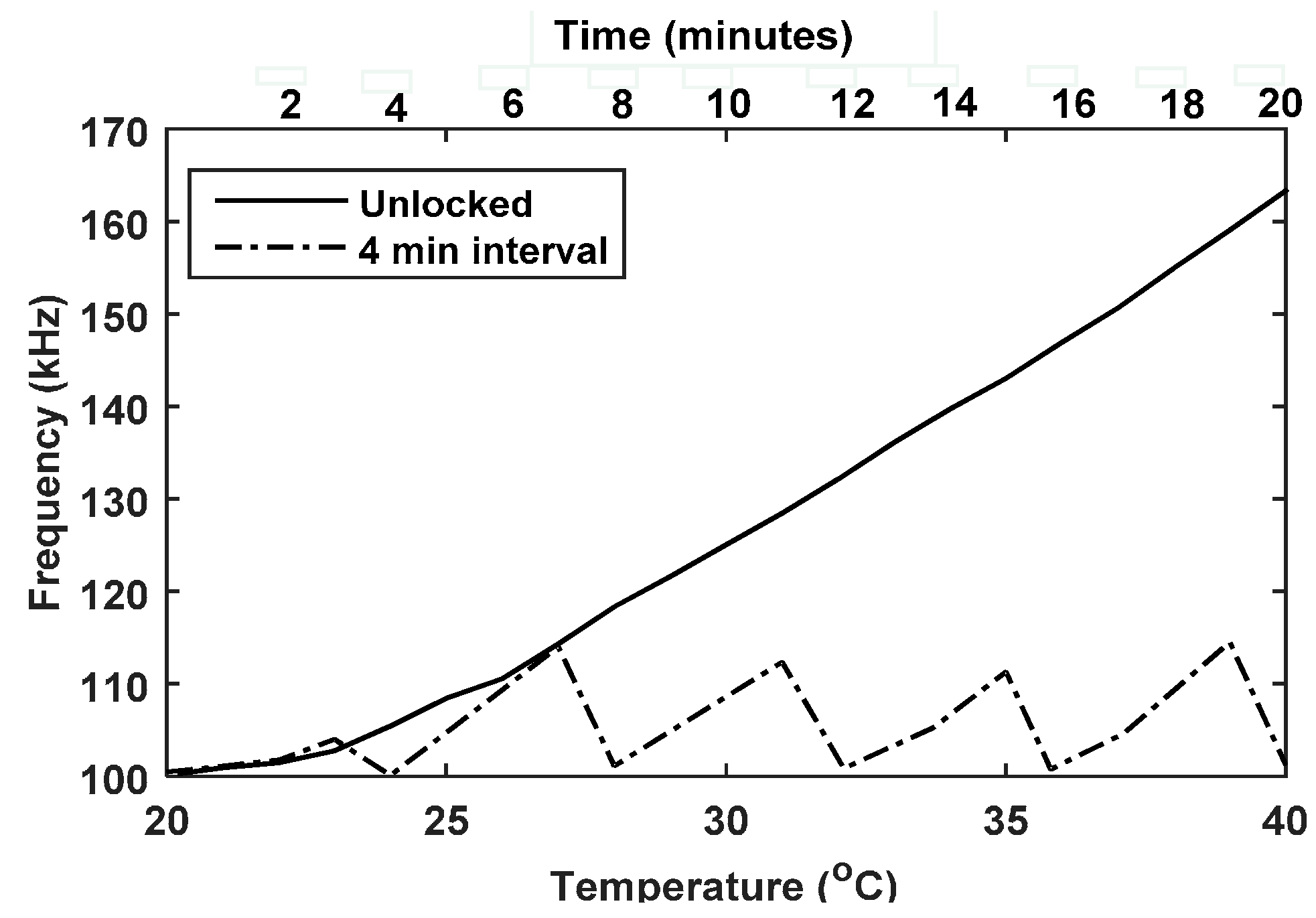
New measurements were made for OSC
ucmp, the uncompensated DCO from [
12], at a lower supply voltage of 0.7 V, for comparison with OSC
diode. Firstly, the measured stability of OSC
diode is 2.51%/°C, which is better than OSC
ucmp, which has a stability of 3.42%/°C at 0.7 V. The previous discussion on the TC explains the above results. The temperature stability of 1.67%/°C stated in [
12] for OSC
ucmp was measured from the test chip implemented in [
12] at 1.1 V supply voltage. In OSC
ucmp [
12], the most significant bit (MSB) for calibration (SAR bits) connects the oscillator delay element directly to
VDD and only the remaining bits connect the oscillator to “off” leaking LVT transistors. Furthermore, the finer delay elements in OSC
ucmp are powered directly by
VDD that causes stability degradation in OSC
ucmp at lower
VDD. Secondly, our new OSC
diode has a power consumption of 20 nW at 100 kHz frequency and 0.7 V supply voltage, which is lower than the power consumption of OSC
ucmp at 35 nW, measured at 0.7 V supply voltage, and 100 nW power consumption for OSC
ucmp at 1.1 V [
12].
Finally, OSC
diode also has an improved voltage stability of 0.1%/mV as compared to OSC
ucmp, which has a voltage stability of 0.6%/mV. Supply sensitivity is discussed further in
Section 3.6. Higher stabilities require lesser re-locking to the stable clock. The above factors make OSC
diode a better candidate for the temperature-uncompensated oscillator in the clock system. The OSC
diode after accurate configuration is used as the system clock meeting the power goals of an ULP system.
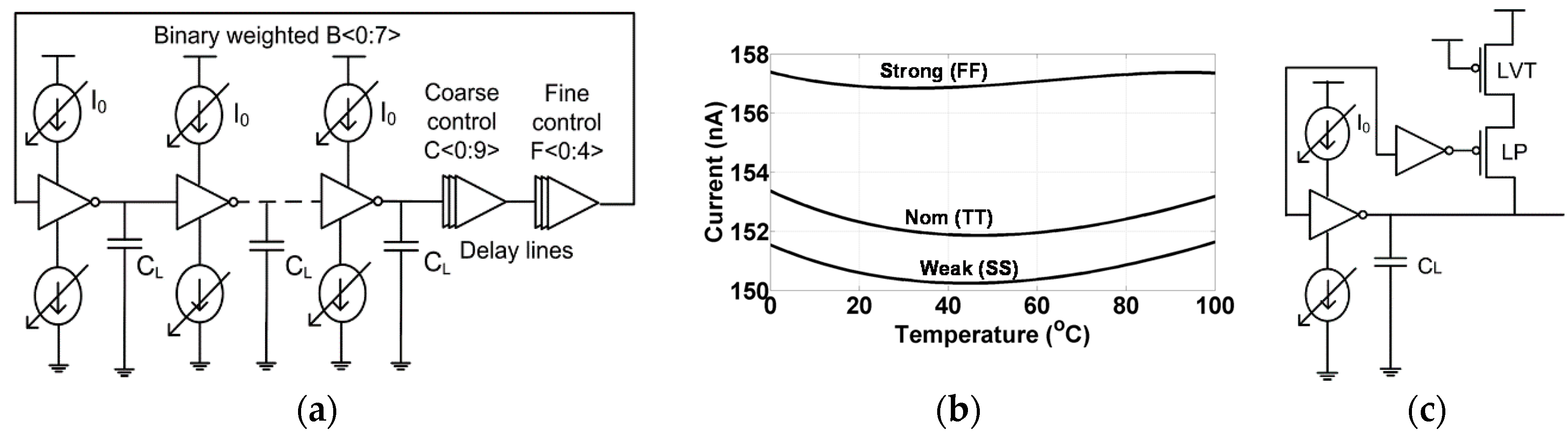
2.2. Temperature-Compensated Oscillator (OSCcmp)
OSC
cmp is a current-controlled DCO implemented in [
12] that is used as a temperature-compensated oscillator in the system. In this paper, we discuss a summary of its key features. OSC
cmp frequency is determined by a constant current source I
o and the capacitance C
L as shown in
Figure 6a [
12].
The constant current source I
o is obtained by adding currents from a Proportional to Absolute Temperature (PTAT) source and a Complementary to Absolute Temperature (CTAT) source [
12]. In the PTAT source, the current increases with an increase in temperature. In the CTAT, the current decreases with an increase in temperature. The sum current I
o of PTAT and CTAT stays constant and it varies by only 1% over a 100 °C range across different process corners (SS, TT, FF,
etc.), as shown in
Figure 6b [
12]. C
L is a Metal-Insulator-Metal (MIM) cap and also has very small temperature variation. Process variation in the current source may cause either the PTAT or the CTAT to dominate the other, making the total current I
o temperature dependent. To balance these currents, the resistance and subsequently the current of the PTAT circuit is configured using 5-bits of process control. To further compensate for the decrease in the period of oscillations at high temperature, a second-order compensation technique is employed. It consists of an off, low threshold MOS, as shown in
Figure 6c, which forms a leakage pull-up path that adds charge to C
L, thereby increasing the delay with temperature. This leakage current is controlled by a 6-bit switch and inverter control, thereby regulating the variation in the off-transistors of the second-order compensation technique. The 5-bit process trimming bits and 6-bit second-order compensation bits are set externally during calibration. Together with the second-order compensation, high temperature stability was achieved for OSC
cmp.
Stability measurements were performed across 10 chips to be 5 ppm/°C from 20 °C to 40 °C (14 ppm/°C from 20 °C to 70 °C) at 1.1 V supply voltage [
12] and 7 ppm/°C from 20 °C to 40 °C at 0.7 V. This DCO is well suited for the human body application temperature range for which it was designed. One such example of a device targeting body temperature range is an RFID batteryless sensor in a wireless human body temperature monitoring system in [
15]. This DCO is operational from 0.7 V to 1.1 V, assuming that once the supply voltage is chosen it is maintained to be stable. This makes it readily usable in ULP nodes employing a wide range of voltages of operation such as [
2].
2.3. Digital Control Block
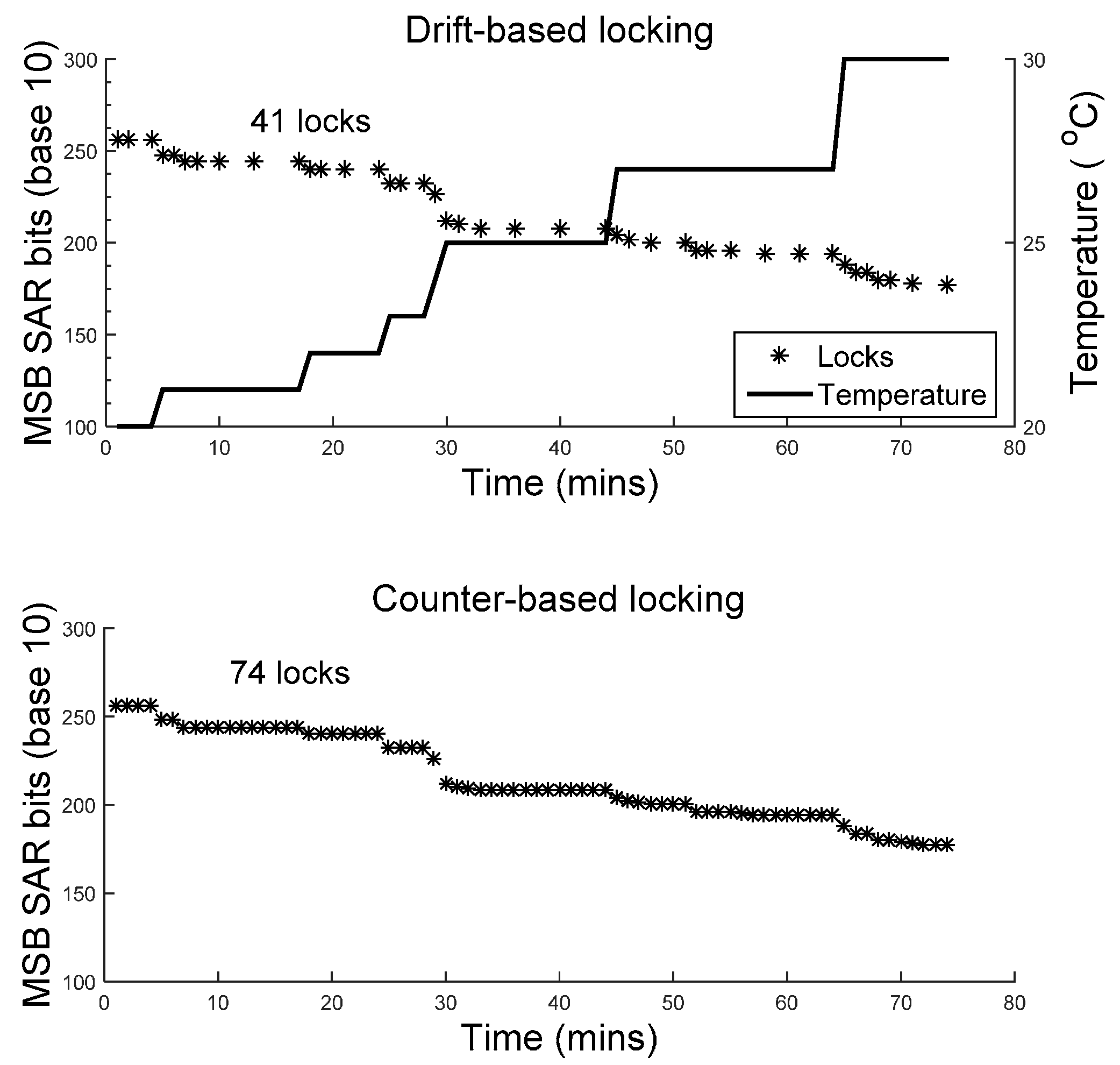
In this work, a low-power digital control block was implemented to automate the locking of OSCdiode to OSCcmp. It controls the time interval between successive locks of OSCdiode to OSCcmp. The digital block is designed using standard digital synthesis flow. We describe two locking modes: (a) a periodic (counter-based) locking scheme; and (b) a prediction (temperature-drift-based) locking scheme in which an algorithm is used to optimize the number of locks in the event of temperature drift. The periodic locking scheme was implemented on the prototype and the prediction locking scheme was verified off-chip. The two modes are described in the following subsections.
2.3.1. Counter-Based Locking Scheme
In the counter-based scheme, locking is achieved through a 32-bit programmable counter. After counting the number of cycles programmed in these registers, the digital block issues a signal to enable the locking of one DCO to another. This programmable counter controls the locking of OSCdiode to OSCcmp in a periodic fashion. A 32-bit count register implies the capability to count 232 cycles. If the digital block is run at the same frequency as that of the clock source (e.g., 100 kHz), the interval between the locking of OSCdiode to OSCcmp can be programmed to be any value between the minimum locking time (3.68 ms), to the maximum time possible (11.93 h) in steps of the clock period (10 µs). After locking, a power-down signal is asserted to disable OSCcmp and save power. Its SAR bits are retained to preserve calibration and frequency lock settings.
The start-up times of all the DCOs are in the range of a few microseconds, which has to be considered during powering up of OSCcmp for the next locking event. OSCcmp must be powered on for a sufficient amount of time before the next round of locking starts to account for its settling time. The digital block takes this into account through a settle register in each counter. A power-up signal is issued at a programmable number of cycles prior to the commencement of the next lock. At a system clock frequency of 100 kHz, 1 settle bit is equivalent to 10 µs, which is sufficient time to start-up OSCcmp. The programmable nature of the count and settle registers in the digital block enables this clock source system to be flexible for serving different application needs. This makes it possible for the system to incorporate another oscillator with lower power or other better clock attributes, and following the above DCO architecture, to be able to easily replace the DCOs described in this paper.
2.3.2. Temperature-Drift-Based Locking Scheme
This locking scheme makes use of the temperature dependence of the SAR calibration bits. As temperature drifts, the frequency of the uncompensated oscillator drifts. When it is re-locked to the compensated clock, the difference in the current and previous value of SAR bits of the uncompensated oscillator indicates the amount of drift in clock frequency and thereby serves as a proxy for the change in the temperature since the last lock.
The SAR calibration bits are designed to be read and write enabled in this system. This makes it possible to read their values from successive locks. During successive locks, if the SAR bits are unchanged or if only the “fine” lower significant bits (LSBs) are changed, it implies that the temperature has not significantly changed since the previous lock. Hence, re-locking, which involves powering up the high-power OSCcmp, leads to unnecessary power consumption. In this prediction-locking scheme, we monitor the bits and perform locks based on the history of temperature change and a prediction algorithm. An algorithm implemented for a temperature drift-prediction based locking scheme is described below.
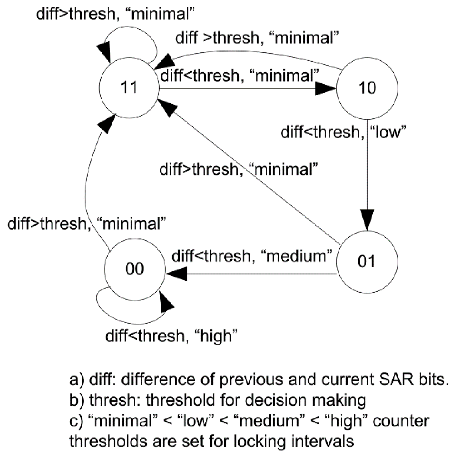
Figure 7 shows the state diagram of the implemented algorithm. The bubbles (11, 10, 01, and 00) represent the different locking states. Each state has a corresponding programmable counter threshold, which represents the time interval between successive locks. A
minimal threshold (corresponding to 11) is the shortest interval between successive locks and a
high threshold (corresponding to 00) is the longest locking interval. The
low and
medium thresholds are intermediate locking interval times and correspond to states 10 and 01, respectively. The SAR bits are monitored every time locking is performed. The initial locking state is “11” corresponding to the
minimal locking interval, because there is no information on the temperature drift in the start. In all the successive locks, the difference between current SAR bits and previous SAR bits (
diff) determines the locking interval. If
diff exceed a pre-programmed threshold value
thresh, it means that a significant temperature drift has occurred.
If diff is greater than thresh, a lock is initiated and the locking state is reset to “11”, causing the next locking and monitoring to take place after a minimal interval. If diff is lesser than thresh, the locking state is decremented by 1, and the next locking happens after an increased time interval (low if the previous interval was minimal, medium if the previous interval was low, high if the previous interval was medium, and stays high if the previous interval was high). If at any point diff is greater than thresh, the locking state flips to “11”, thereby resetting the state machine. The circuit implementation of the algorithm was achieved using a digital synthesis flow. The functionality and power savings of the algorithm was verified using simulations, but was not implemented in the prototype. However, the reading out of SAR bits and variable locking intervals in this scheme was verified using chip measurements by implementing the algorithm in software.
The digital block is operational at voltages ranging from 0.5 V to 1.1 V for a 100 kHz system frequency. For a count of 1 min, the measured power consumption of the digital block is 12 nW in the counter-based locking mode. The estimated power consumption of drift-based locking mode from simulations is 5.1 nW at 100 kHz with 0.7 V supply voltage. The power consumption for the temperature-drift-based locking mode is obtained from simulations because it was not implemented in the prototype. Operating the digital block at a lower frequency using a divided clock can further minimize this power consumption. To achieve the same locking interval time at a lower operating frequency, fewer
count bits need to be set thereby lowering the switching activity. Further, if the digital block is run at a divided clock of 50 kHz, it can even be operational at 0.4 V supply voltage. At 50 kHz and 0.4 V, its power consumption goes down to 730 pW for the same locking interval and the power consumption of the overall clock source system in this case is 25 nW. Since there are only two signals (reset and power-down) interfacing the digital block to the oscillators and they toggle only once during each lock, they may be level-shifted to the oscillator domain without much loss of power. Hence, it is advantageous to operate the digital block in a sub-threshold voltage domain, which is usually available in ULP systems such as [
2].
2.3.3. Power vs. Stability Analysis
The proposed programmable system allows us to analyze the power-stability trade-off, which we present in this subsection. We define the following parameters for our analysis:
Pdiode: OSCdiode stand-alone power.
Pcmp: OSCcmp stand-alone power.
Pdiode_lock: OSCdiode power during locking (It is different from Pdiode).
Pcmp_leak: OSCcmp leakage power.
Pdig: Digital block power (includes both active and leakage power).
Tcmp_settle: OSCcmp settling time after it is turned on (before the next locking commences).
Sdiode: OSCdiode stand-alone stability.
Scmp: OSCcmp stand-alone stability.
Tinterval: Time interval between consecutive locks.
Rtemp: Rate of temperature change.
Tlock: Total duration for all locks.
Tnolock: Total duration when no locking takes place.
Ttotal: Sum of Tlock and Tnolock.
Tduration: Time duration of each lock.
OSC
diode and digital block are “ON” for the whole duration, while OSC
cmp is “ON” only for the duration of the lock. The total system power consumption (P
total) can be estimated to be:
The digital block controls T
interval, which relates to T
lock in Equation (1) as:
During no lock conditions, the oscillator frequency drift is given by D
diode_nolock for OSC
diode and D
cmp_nolock for OSC
cmp.
In the duration of T
total, the total number of locks are
n = T
total/T
interval, where n is an integer. At the end of these locks (at time n × T
interval), OSC
diode would have only drifted in the worst case as much as OSC
cmp. During the remaining time (T
total – n × T
interval), the frequency drifts at the original rate for OSC
diode. The effective frequency drift during T
total can be estimated as:
The maximum drift of frequencies between each lock (MaxD
diode_lock) is one approach to get the maximum frequency variation of the clock. This is equivalent to the net frequency drift during time interval between each lock (T
interval):
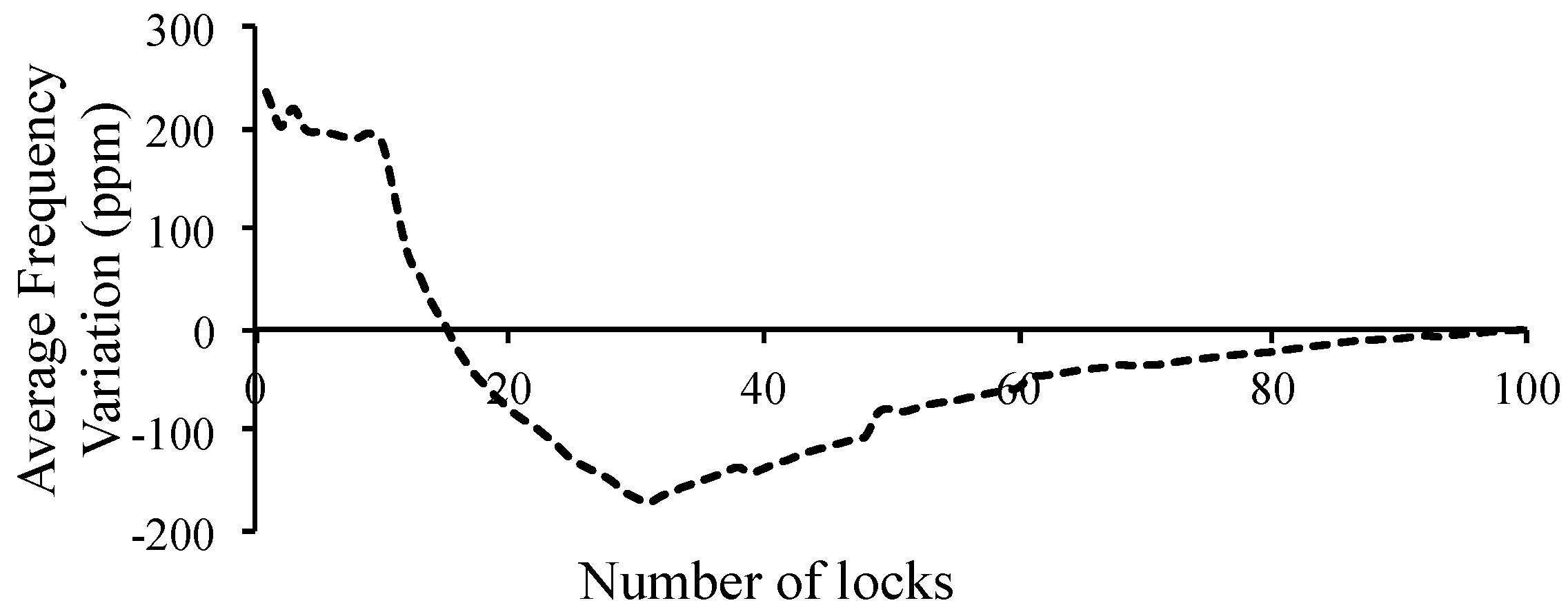
From Equation (12), we observe that MaxDdiode_lock decreases proportionally with Tinterval. Using the above equations, we are able to calculate the maximum frequency drift for any power budget, or the power consumption for any stability budget. If the rate of locking is greater than the rate of temperature change, the system power increases with no additional improvement in stability. This is because the stability of OSCdiode cannot exceed the stability of compensated oscillator OSCcmp.


