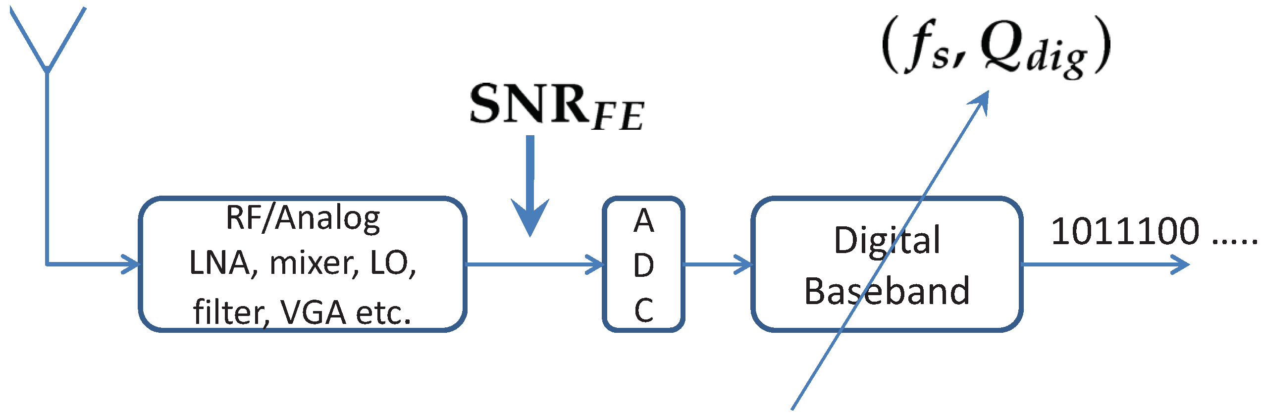
Power Scalable Radio Receiver Design Based on Signal and Interference Condition

Abstract
:1. Introduction
 MHz with DSSS physical layer with OQPSK modulation specifies
  dB possible variation in the received signal strength. We take advantage of this large variation by designing a power scalable baseband architecture, which adapts itself to the variation in signal and interference levels. The digital section adapts the word length (
  ) and sampling frequency (
  ). To make the receiver adaptive and low power, various design techniques are proposed in this paper. The key features of this power scalable receiver are interference detector and SNR estimator (IDSE), variable tap and variable coefficient FIR filter, an adaptivity control unit and an adaptation procedure. of the receiver to minimize power requires varying number of taps in the FIR filter. Authors in [1] have proposed a variable tap FIR filter based on approximate filtering to reduce power. In doing so, authors have demonstrated power reduction by a factor of 10. Besides varying number of taps to save power, we have used minimum resolution coefficients for FIR filters to save power. Author in [2] controls the resolution of analog-to-digital converter (ADC) in receiver and digital-to-analog converter (DAC) in transmitter. The ADC resolution is controlled depending on signal-to-noise and signal-to-interference ratio and resolution of DAC is controlled based on crest factor of modulation scheme. The author has not suggested any way to measure signal-to-noise and signal-to-interference ratio. Authors in [3] have proposed reconfigurable radio for MIMO wireless systems. Authors have emphasized on optimizing number of operations, latency requirements and the architecture of signal processing elements to minimize complexity of the MIMO signal processing. Number of antennas and modulations levels are reconfigurable in the systems proposed in [3]. Adaptive word length control is used to implement an OFDM based low power wireless baseband processing system [4]. OFDM processing essentially consists of filtering, followed by an FFT engine and then an equalization block. The Error Vector Magnitude (EVM) of the received signal is continuously monitored, to adjust the word length. If EVM is above a threshold, the word length is increased to improve precision and conversely, for good EVM (low error rate), the word length is reduced. Our approach for receiver design incorporates controlling the amplitude quantization and sampling frequency depending on the SNR levels and interference presence. Our approach of scaling power by varying and applies the concepts of adaptive signal processing to minimize power. Traditionally, adaptive signal processing is well known for minimizing error of signal processing structures [5], whereas our objective is to minimize power while keeping the error criteria as a constraint in the optimization formulation. An adaptation procedure is proposed to facilitate adaptation in packetized communication.
 mA when active with
  V power supply. Low power analog front end design for IEEE 802.15.4 has been proposed in a few papers [7,8] . In [7], authors proposed a front end design in
 CMOS technology that consumes
  mW, whereas in a more recent paper the authors in [8] proposed a front end in 90 nm technology that consumes
  mW when active. Authors in [9] have discussed power consumption of various wireless technology for WPAN applications. As mentioned, authors in [9] say that the power consumption of wireless devices scales with the data rate. Typically, IEEE 802.15.4 receiver consumes mA for
  Mbps,
Mbps,  mA for Bluetooth at
  Mbps,
Mbps,  mA for WLAN at
  Mbps. Power consumptions in analog and digital portion separately have been reported in some papers. Authors in [10] have reported that baseband of IEEE 802.15.4 consumes
  mA at V supply (
  mW) in m technology whereas the analog portion consumes
  mA. The authors in [9] have given break up of analog and digital portion of the receiver for UWB. Here analog portion consumes mA compared with
  mA of digital at
  MHz. and for the digital baseband. Following this we explain our approach to minimize power based on this optimization. Section 3 explains the simulation and interference model used in subsequent sections. Section 4 discusses various blocks of the receiver, which are designed to accommodate variable and and to be compatible with adaptation procedure. Section 5 discusses the implementation specific details and dynamic power estimation of the design. Section 6 discusses experimental setup and results from the experimental setup to validate the concepts. Section 7 concludes the paper.
2. Power Scalable Digital Baseband
2.1. Optimizing Power
and of the digital section.
 is the SNR seen at the input of the ADC. It is the ratio of total signal power to the total noise power. It should not be confused with Eb/No typically used in communication theory literature. Input of the ADC, consists of the signal and the noise. We have assumed a 2nd order Butterworth bandpass filter preceding the ADC. The noise present at the input of ADC also has out of desired signal band components. This makes negative when noise is high. The packet error rate (PER) requirement translates to BER of
  [11]. and are chosen to minimize power while achieving target BER. More formally:

 and , if these parameters are chosen very high. In such a case the implementation of digital portion does not alter the SNR calculation of the receiver, i.e., SNR seen at the input of the ADC is almost the same as SNR seen at the input of the demodulator. But in doing so the digital portion is over-designed and hence wastes power. In order to achieve a given BER, there can be different combinations of and for a given and interference levels, each with its own power cost. Values of and that minimize power as given in Equation (1) will be used. Furthermore, with varying values of and interference, the optimal choices for and can vary, necessitating an adaptive resolution based digital section. For different levels of and interference, the optimal design parameters (
  ) will be stored in the LUT and used to configure the receiver. Finding a closed form expression for the function “
  ” in Equation (2) is hard due to the non-linear relationships. Coarser the ADC quantization
  , harder it becomes to analyze the signal. Hence BER is found through MATLAB simulations, for different ( ) values. The power function in Equation (1) is obtained by Synopsys Prime Power for different and values. Finally, the optimum and values are obtained by a simple search over design space.
2.2. Proposed Architecture and Functioning
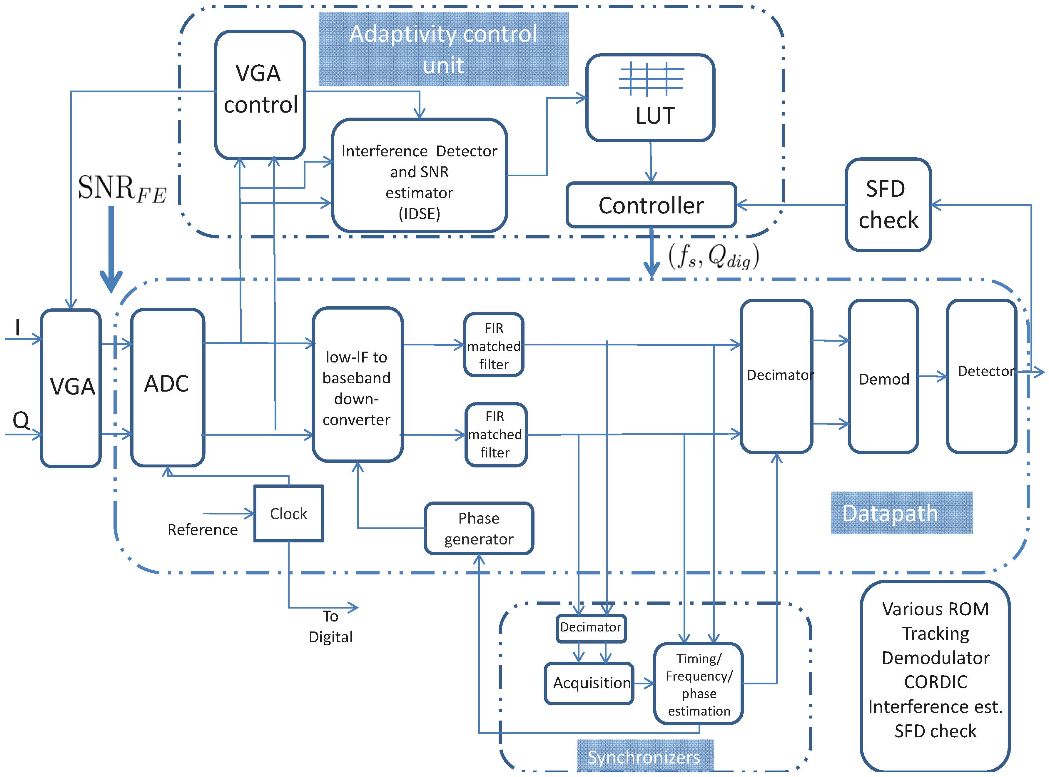
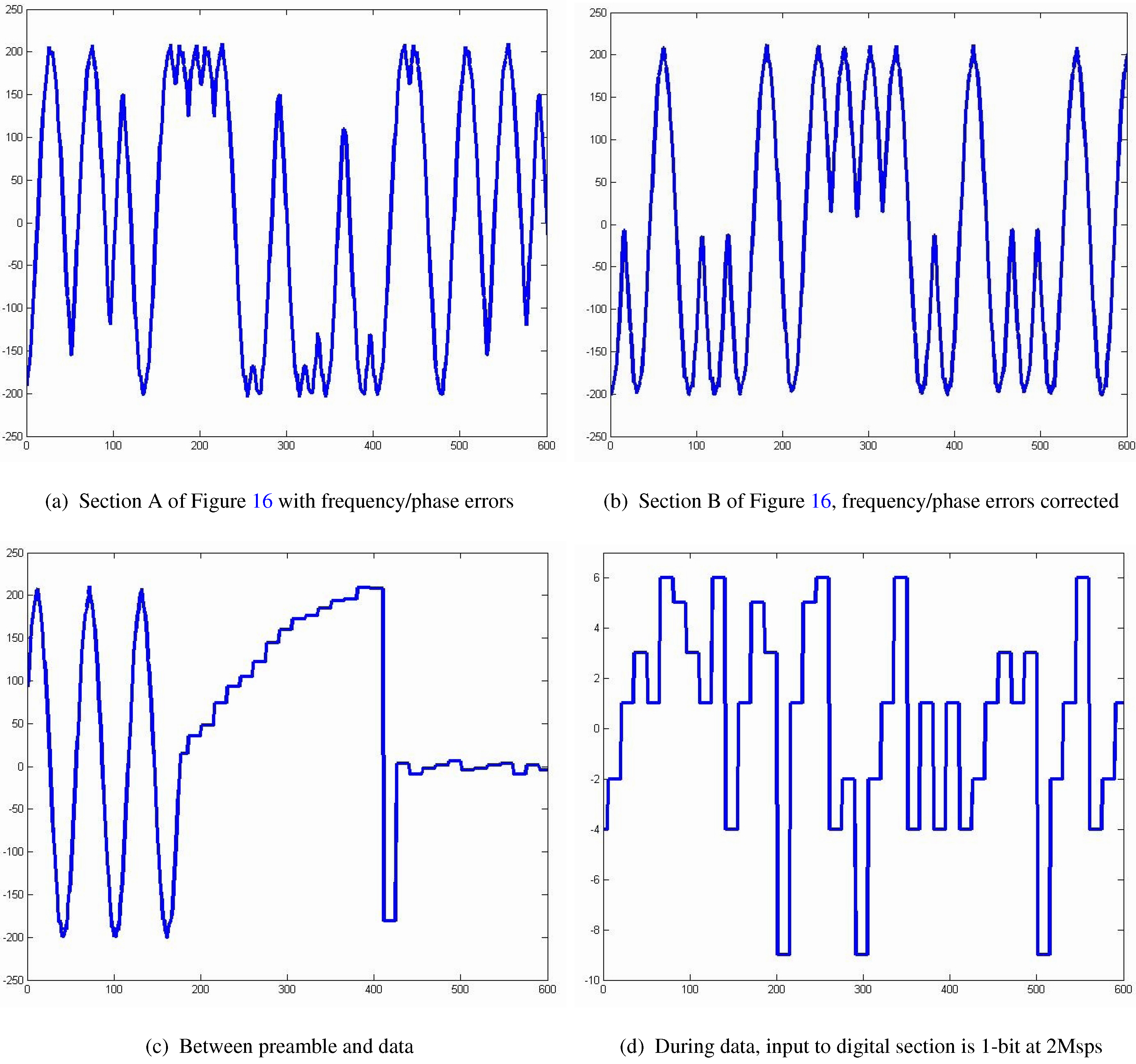
and of different sections of the receiver. For every packet the receiver starts off with the highest resolution and sampling frequency settings during the packet preamble. Synchronization (Timing, Frequency, Phase) is done with the highest settings and simultaneously, the interference and signal levels are estimated. By the end of the preamble, a LUT containing optimal values is consulted and the optimum and is used for the rest of the packet reception. All sections of the receiver in Figure 2 except the VGA and ADC are implemented in HDL for power estimation. is sampling frequency and is word length. and . The first setting as shown in the Figure 3 ( Msps,
  -bit) is the setting of word length and sampling frequency for the receiver during preamble of the packet. The second setting ( , ) applies for rest of the packet, i.e., PHY service data unit (PSDU).
 and
and  ; (6) Start-Frame-Delimiter (SFD) check; (7) Decimate, demodulate and detect at
  and
and  .
and ; (6) Start-Frame-Delimiter (SFD) check; (7) Decimate, demodulate and detect at and .
.
and ; (6) Start-Frame-Delimiter (SFD) check; (7) Decimate, demodulate and detect at and .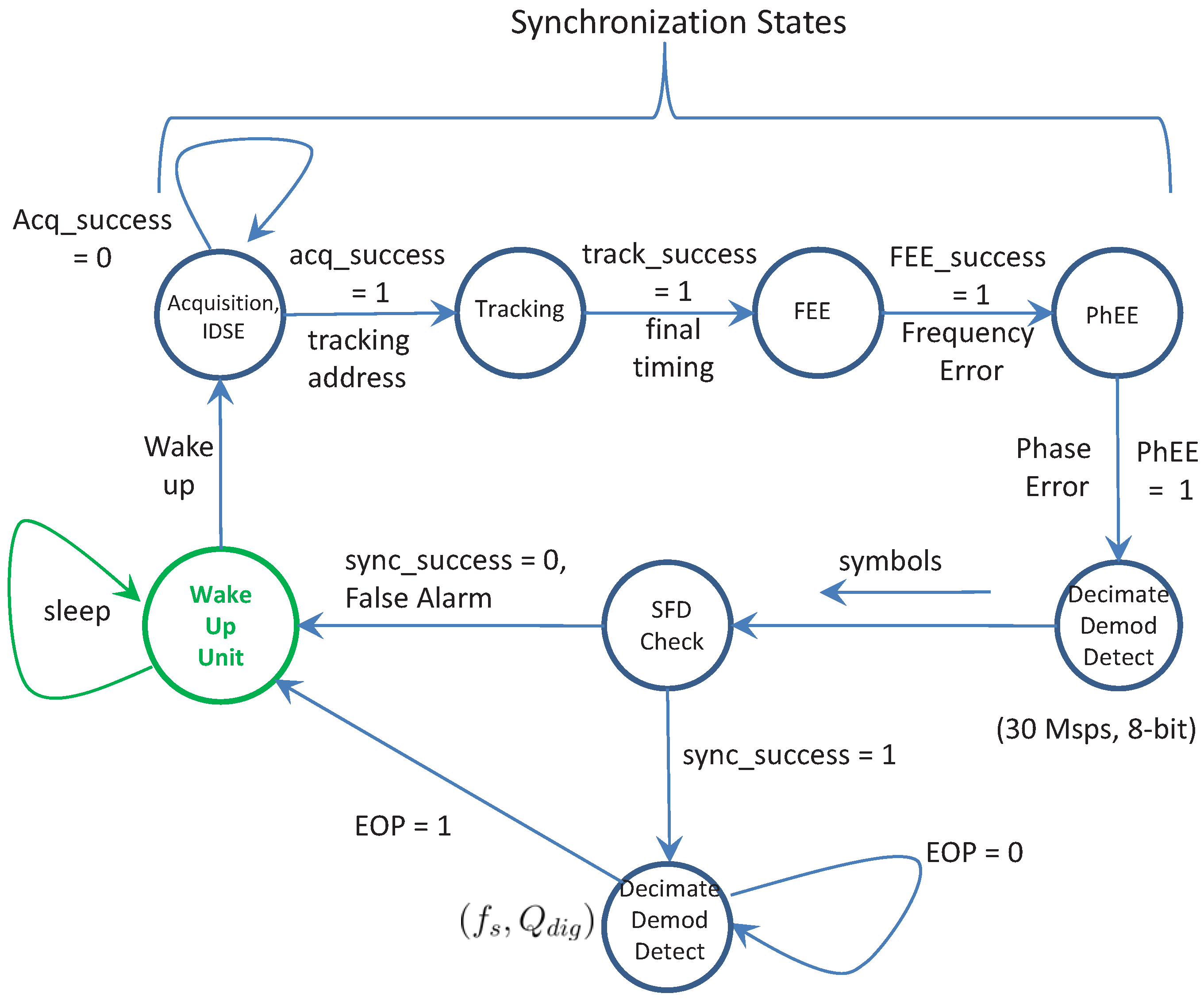 is high. The synchronization designed for this receiver works on the continuous flowing sampled data from ADC. Figure 5(a) shows the typical buffered implementation of a receiver. Here, various signal processing blocks inside the receiver access the data from the buffer. This allows the receiver algorithms to reuse the data and gives better convergence performance. However, our approach for the receiver design does not use any buffer to save area and power. Figure 5(b) shows the non-buffered approach. Here, besides passing information regarding completion of its functioning as discussed above, every module passes a sample index to the subsequent module. For, e.g., acquisition unit passes acq_success and a count track_address to the tracking block once acquisition is done. The tracking unit initiates a counter when acq_success is received. The counter counts number of samples and the tracking begins when the counter reaches the count track_address. Once the synchronization is done (
  ) is raised, all synchronization blocks turn off and receiver data-path (NCO, Matched filters, decimator, demodulator and detector) adjusts itself to new settings of and
  = MHz, = -bit.
  —1 to 30 MHz. —1 to 8 bits.
= MHz, = -bit. —1 to 30 MHz. —1 to 8 bits.
—1 to 30 MHz. —1 to 8 bits.
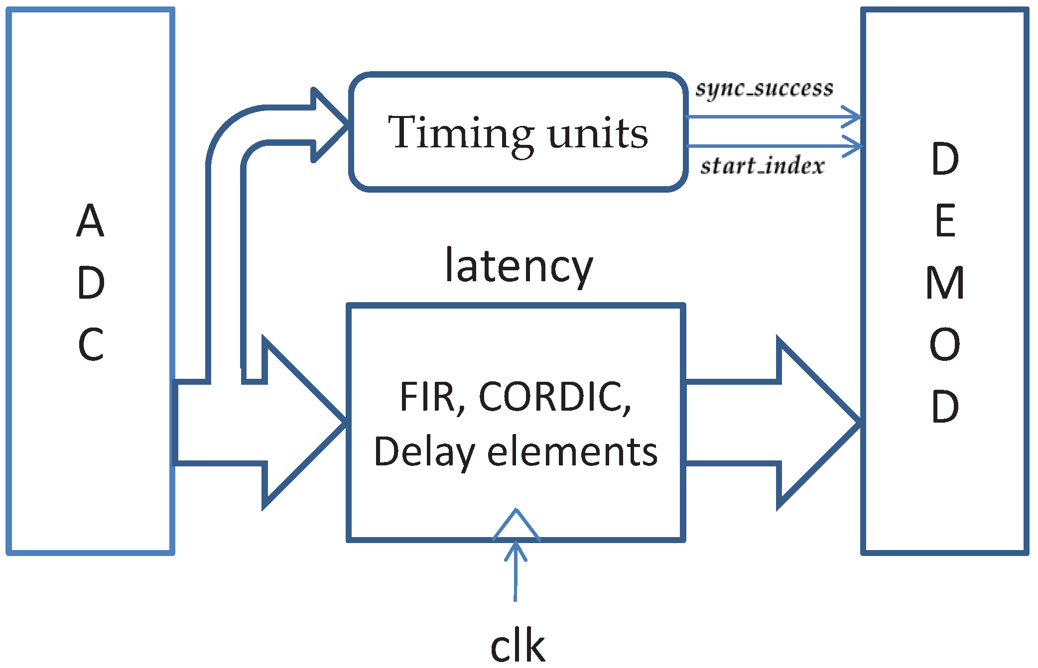
= MHz, = -bit. —1 to 30 MHz. —1 to 8 bits.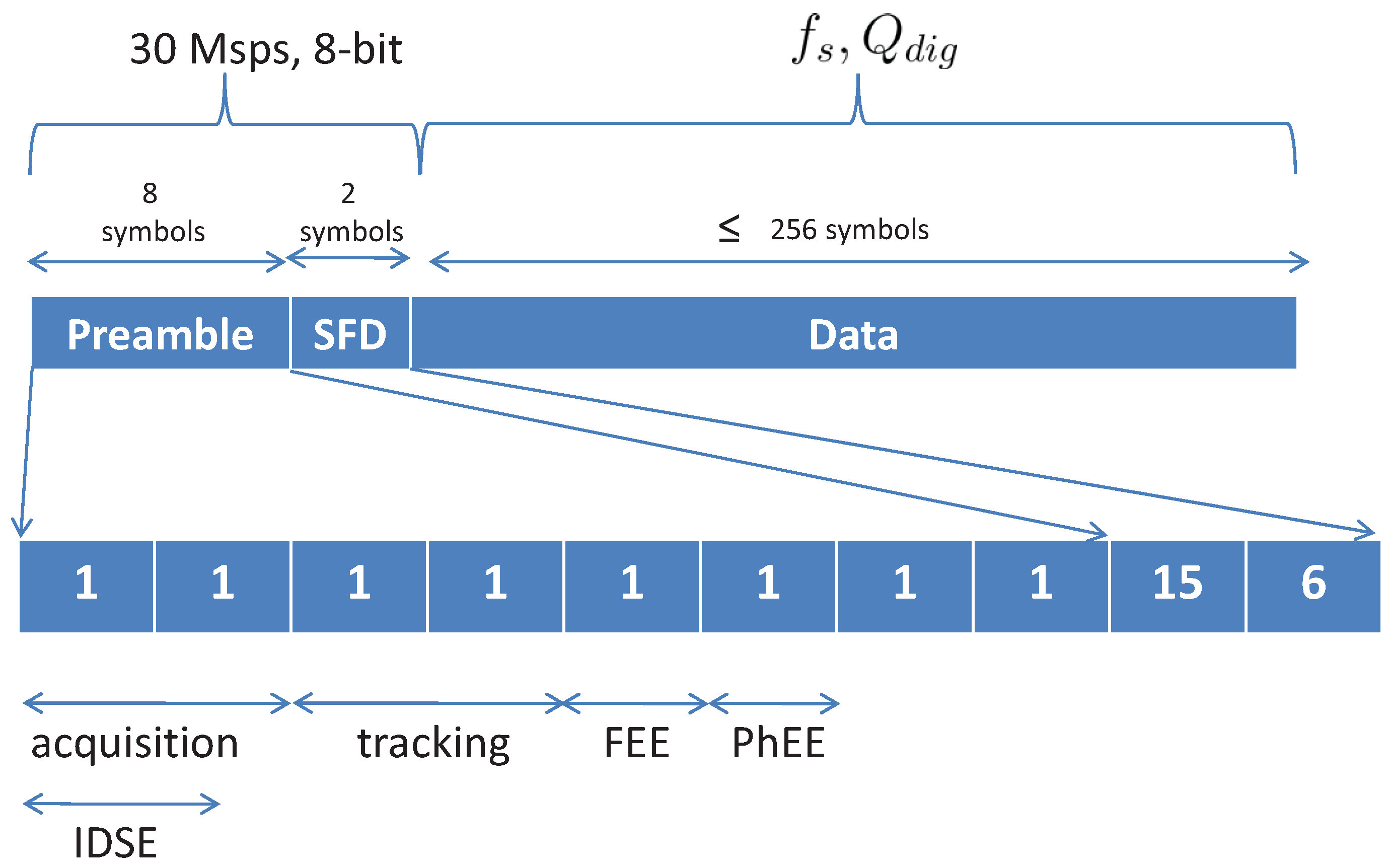 and , it is proposed to discard all samples in delay elements across the receiver. This is due to the fact that the samples in delay elements across the receiver is sampled at higher sampling frequency than the new assigned and for the data duration. Delay elements are reset when the adap_ctrl goes high. As shown in Figure 6, once the sync_succ goes high, demodulator waits until the sample_index reaches start_index. Value of start_index is equal to number of clock cycle delay from output of ADC to demodulator.
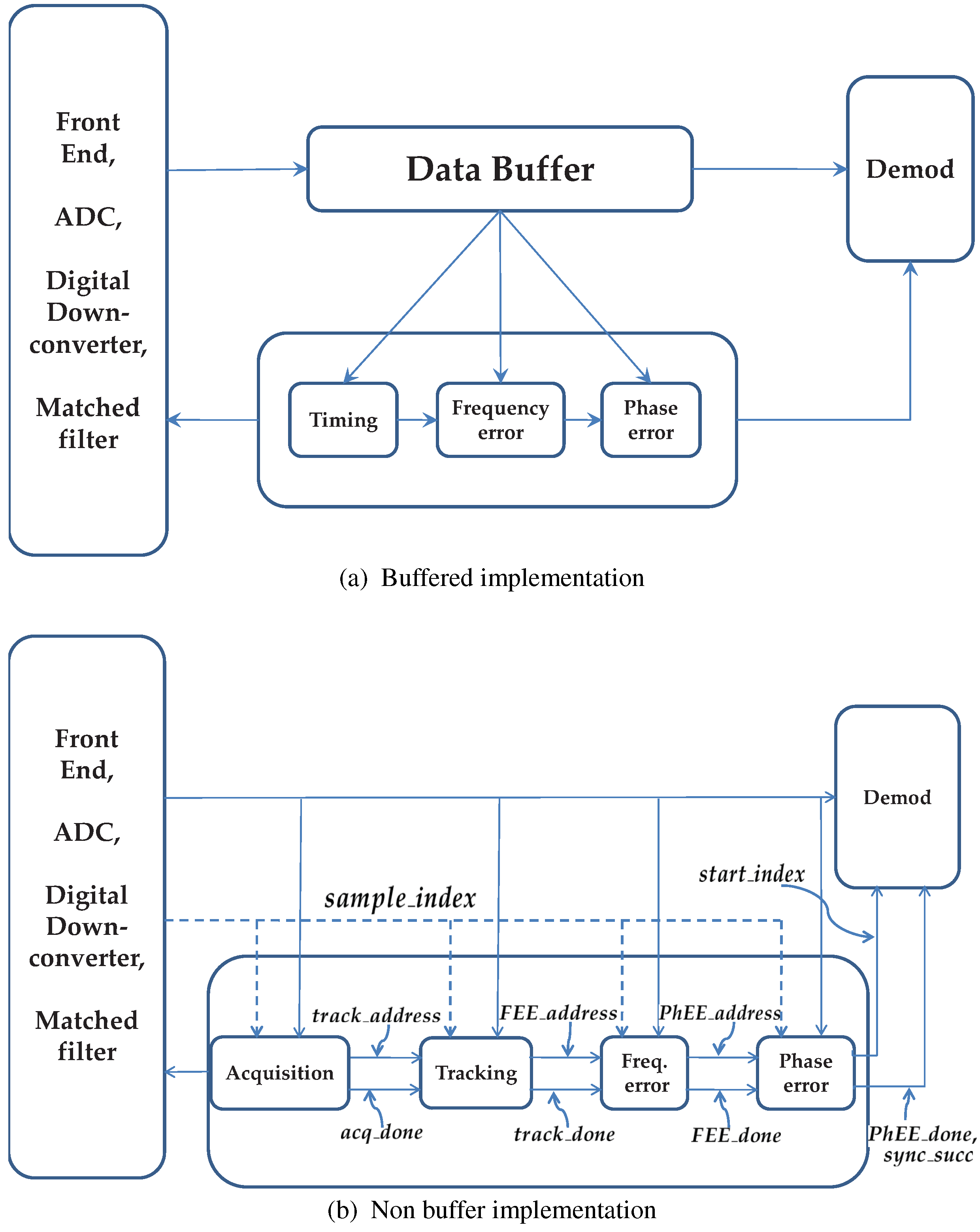
3. Determining Optimal LUT
and interference, we evaluate BER of the receiver for several different settings of and .3.1. Simulation Model
at the input of ADC. Amplitude and time resolutions of ADC and digital baseband sections are variable. is the variable gain of VGA, and are sampling frequency and bitwidth respectively.
is the variable gain of VGA, and are sampling frequency and bitwidth respectively.
is the variable gain of VGA, and are sampling frequency and bitwidth respectively.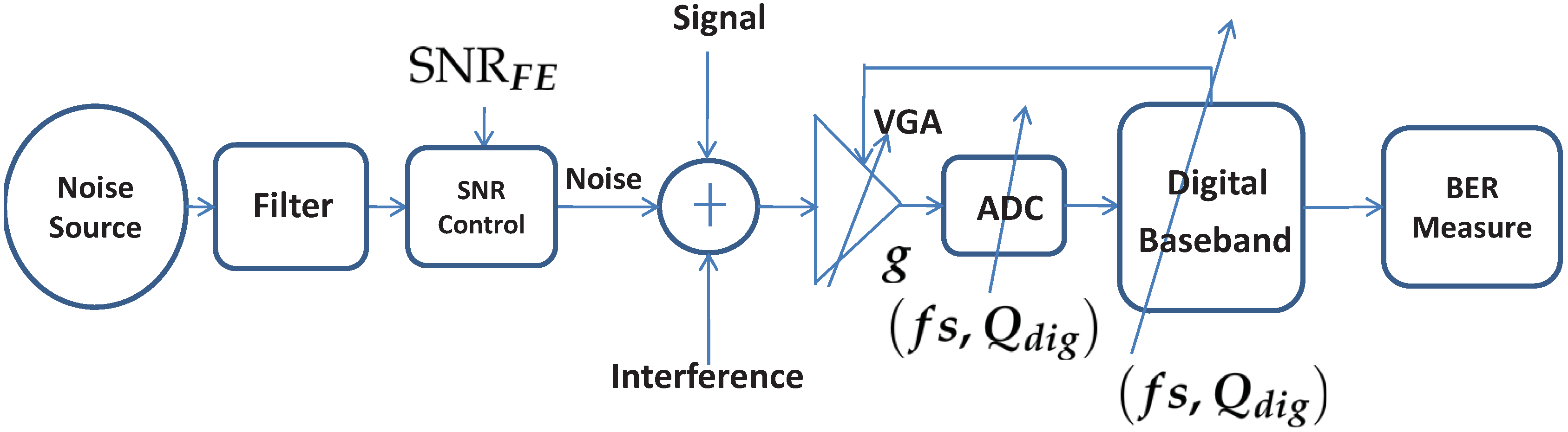
3.2. Interference Modeling
 dBm, whereas alternate channels should be considered transmitting
  dBm. Adjacent channels are
  MHz apart from the desired channel on either side. Similarly, alternate channels are MHz apart. For an IF of
  MHz [16], input to the ADC can be given as

 is the desired baseband signal.
  and
and  are adjacent baseband signals.
  and
and  are alternate baseband signals. and can be very time consuming [17]. Instead we have developed a technique to reduce the computation time. Initially we find the variance of correlations at the output of correlation demodulator. We use the same variance measure in our subsequent simulations with different receiver settings. We found that this technique reduces the simulation complexity lot in comparison with doing BER simulations with bandpass signals.
4. Implementation Details
4.1. Interference Detector and ![Jlpea 02 00242 i022]() Estimator (IDSE)
Estimator (IDSE)
 is the power measured in adjacent channels,
  is the total power in alternate channels and
  is the power in the desired signal’s channel.
4.1.1. Interference Detector
. For all three states, setting of NCO is changed to down-convert adjacent or alternate or desired signal. IDSE consists of two arms, one each for one adjacent or alternate channel. Only one arm is active during estimation. Both arms have a CORDIC NCO unit to down-convert the interference or signal. Output of detectors/estimator goes to a comparator that compares it with threshold. For interference detection, output of comparators is 1-bit to indicate presence of interferences. In estimator mode, comparator finds the range in which the measured falls. LUT has SNR steps with difference of  dB. Since SNR variation can be up-to
  dB so it has SNR steps, requiring 6-bit index. There are four possible combinations from interference detection: Alternate present/absent and Adjacent present/absent, it is indicated by
  bits. So, LUT is indexed by -bits.
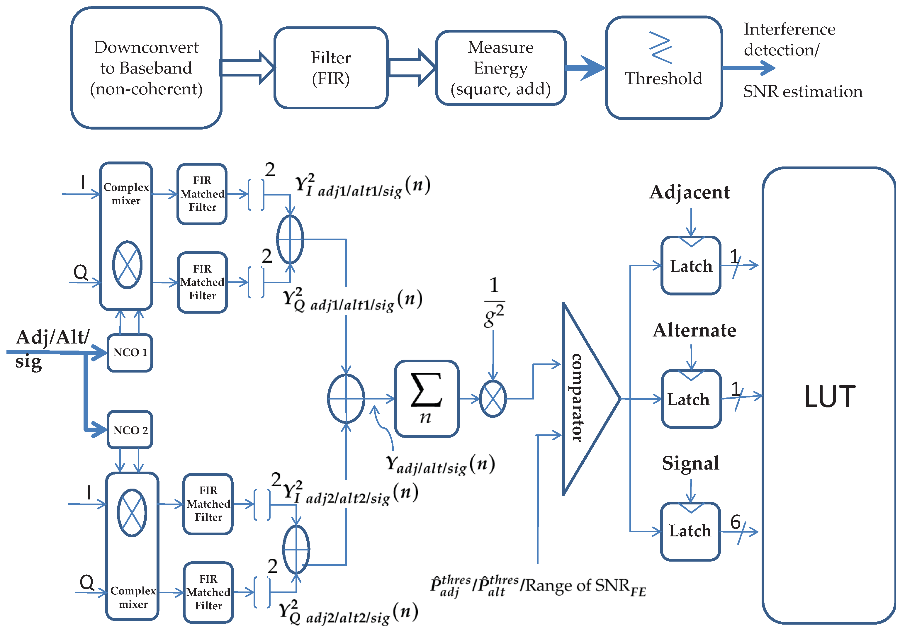 MHz and MHz distance is approximately
  dB. When measuring the desired signal power, due to attenuation by the matched filter, adjacent signal level falls to
  dB and alternate signal level falls to
  dB. These levels of interference are quite low and do not corrupt the signal power estimation. Whereas, while measuring interference power, signal power from desired band can affect the interference power measurement. This is due to the fact that the maximum possible signal power is
  dBm and it can spill to neighboring bands. At such high signal level even after the attenuation by the matched filter, its strength in neighboring channels is high enough to affect interference power measurement.
 and
and  be the in-phase and
  and
and  are the quadrature phase adjacent channels. These terms are analogously defined for alternate channels too. is the gain of VGA [18,19]. Measured power in adjacent and alternate channels (
  ) can be defined as:


 exceeds a-priori calculated threshold,
  , then adjacent interference is detected. Similarly,
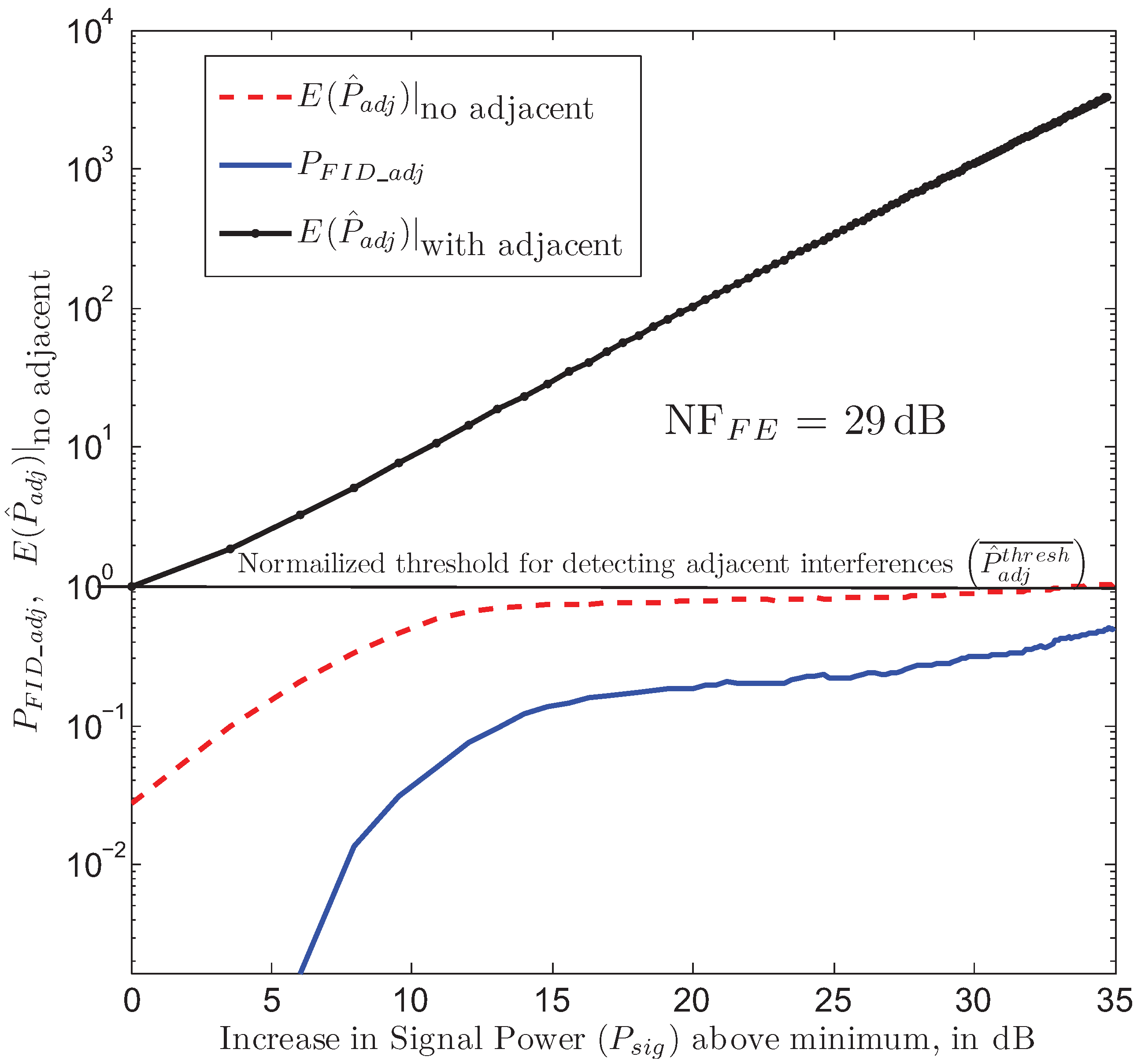
  is the threshold what is compared with . Figure 10 shows the effect of desired signal power on adjacent channel interference detection. The figure is obtained for front end noise figure (
  ) of
) of  dB [20].
  is the normalized threshold for detecting presence of adjacent interference. When signal power is large, then even in absence of adjacent interference, can exceed .
  in figure is probability of false adjacent interference detection. increases with increase in desired signal strength. When signal power is more than dBm, then even in absence of adjacent interference
  exceeds . As shown later, when
  is high (
  ), and settings of receiver is a minimum irrespective of outcome of interference detection. Effect of is less severe on detecting alternate interference as alternate channels are farther in frequency domain. Variance of interference detector reduces with increase in number of pulses utilized for detection. Interference detection is done over four half sine pulses, as the variance does not change much for further increase in duration of detection. = dB. Minimum =
  dBm. NF is calculated for minimum . As figure shows, large desired signal power hinders accurate interference detection. But as evident from Table 1, accurate interference detection is needed until is dB above minimum. of
  dB corresponds to
  dB .
= dB. Minimum = dBm. NF is calculated for minimum . As figure shows, large desired signal power hinders accurate interference detection. But as evident from Table 1, accurate interference detection is needed until is dB above minimum. of dB corresponds to dB .
dB .
= dB. Minimum = dBm. NF is calculated for minimum . As figure shows, large desired signal power hinders accurate interference detection. But as evident from Table 1, accurate interference detection is needed until is dB above minimum. of dB corresponds to dB .
4.1.2. SNR Estimation


 and
and  are given by
  , where
  is AWGN, then

 ,
,
 , Equations (8) and (9) can be used. Front end of the receiver is designed for a constant noise figure. Thus the worst case variance of noise
  contributed by the front end is known. Hence, SNR can be estimated using Equation (11). estimator is ON for one symbol duration.
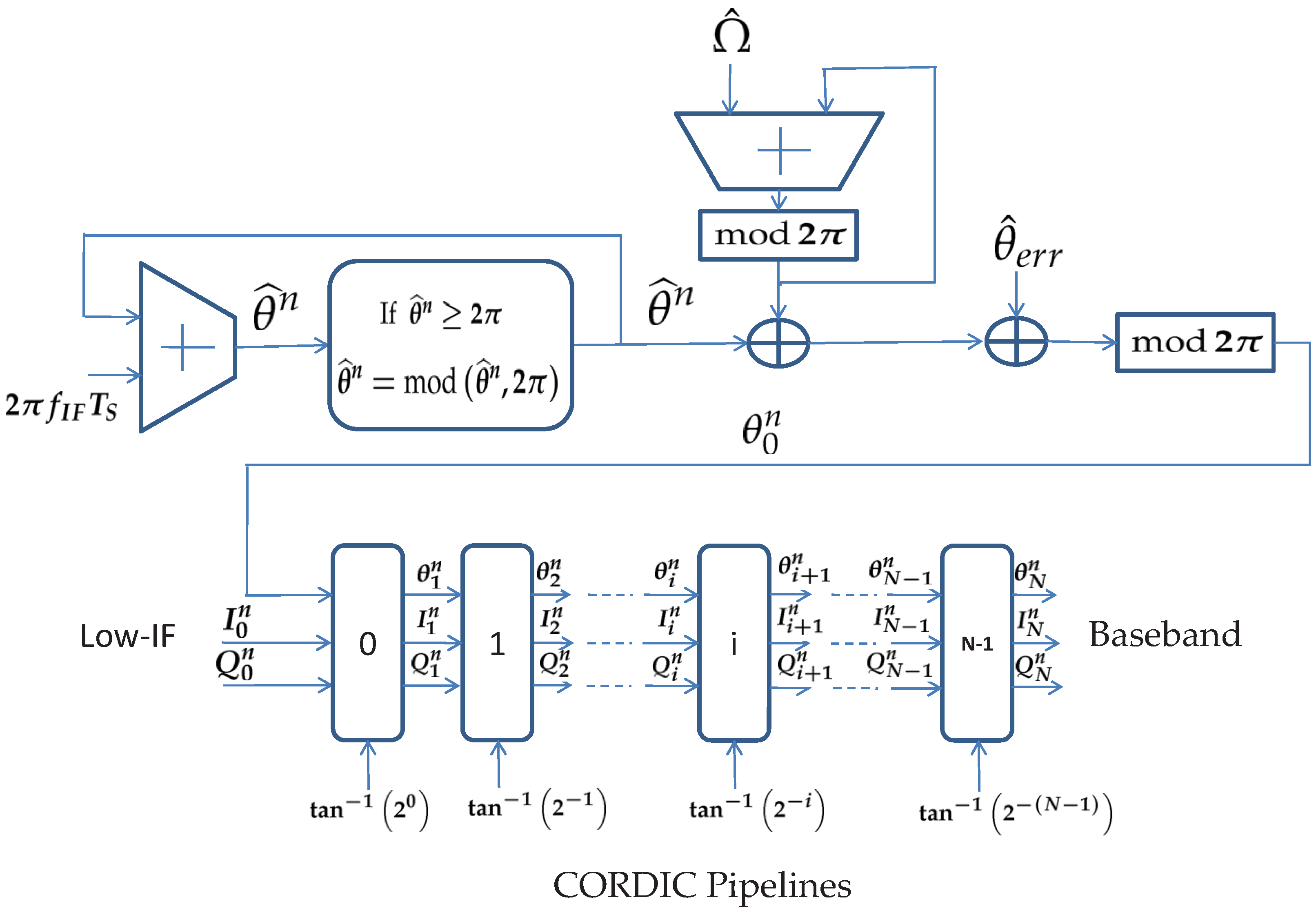
4.2. CORDIC Down-Converter and Phase Generation for CORDIC Blocks
 , which is fed from LUT.
, which is fed from LUT.
, which is fed from LUT.
 bits. Number of pipeline stages and word length for phase representation are optimized based on analysis in [22], with the constraint that errors introduced by quantization in above two parameters should not corrupt a full length packet.
  is the estimated frequency error generated by FEE.
  is the phase error estimated by PhEE.
4.3. FIR Filter, Decimator and Demodulator
4.3.1. Adaptive FIR Filter
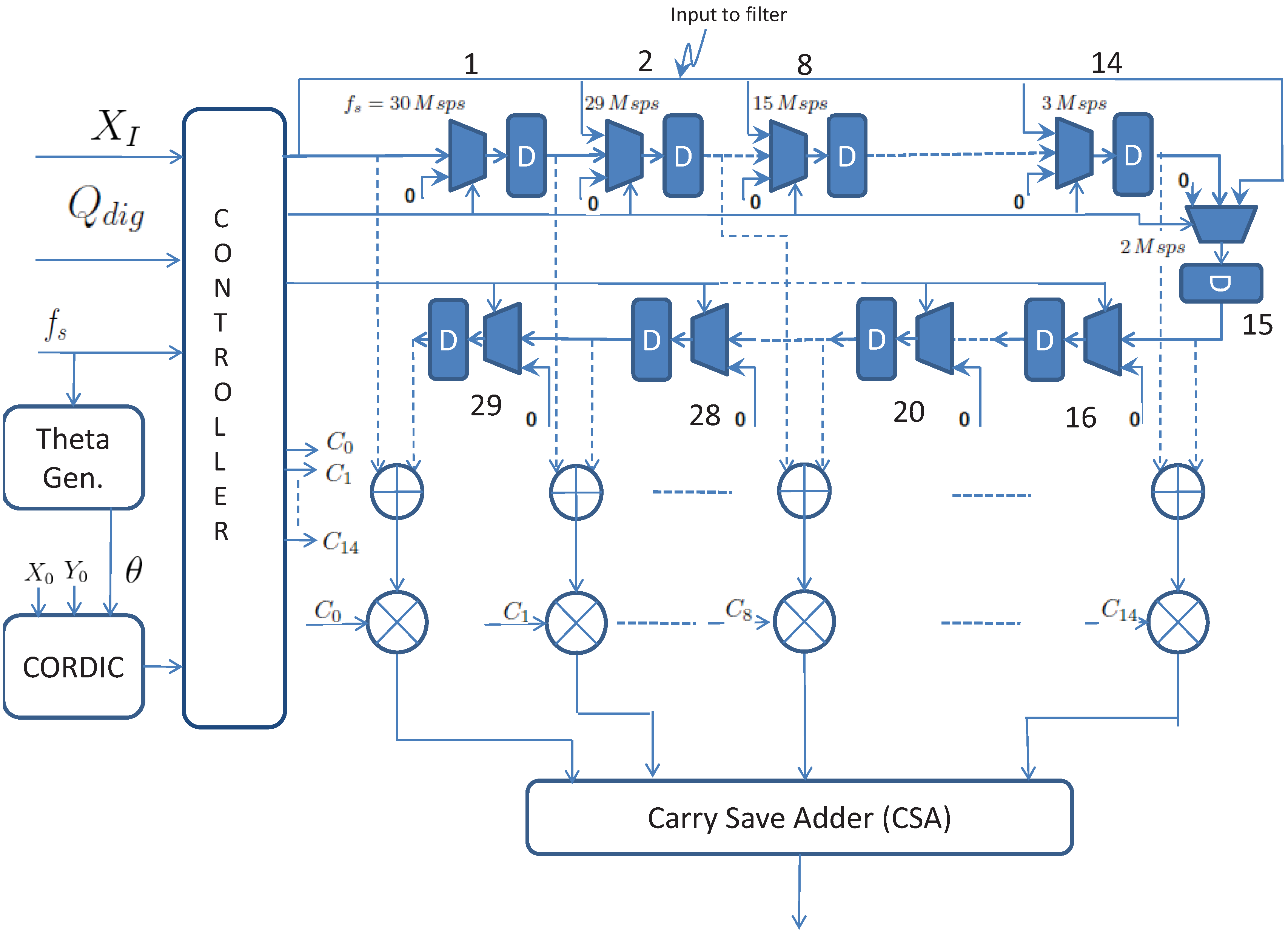
taps (corresponding to maximum sampling frequency). The CORDIC unit generates FIR coefficients that are input to multipliers. The theta generator supplies phase values to CORDIC unit to generate coefficients. Generating FIR coefficients with CORDIC makes it more amenable to adaptive architecture. The phase values depend on . Resolution of coefficients are controlled based on . controller controls the word length of FIR coefficients. Multipliers are Baugh–Wooley multipliers.
controller controls the word length of FIR coefficients. Multipliers are Baugh–Wooley multipliers.
 multiplexer. Depending on the sampling frequency, either a zero or output of the preceding delay element or input to the FIR filter is multiplexed to the input of delay element. As shown in the figure, when the sampling frequency is Msps, delay elements numbered 14 and 15 are active and all other delay elements have zero inputs. Multipliers corresponding to inactive taps get zeros at its input and hence have no dynamic power. The carry save adder adds outputs of the multipliers.
4.3.2. Decimator, Demodulator and Detector
5. Implementation and Power Estimation
 -nm UMC CMOS process for maximum sampling frequency of Msps using Synopsys Design Compiler. The power estimation is done once post synthesis simulation is successful. Synopsys Prime Power is used for estimating dynamic power. Input to Prime Power is the VCD (Value Change Dump) file generated from verilog simulation and the synthesized netlist. The VCD file contains all signal transition that occurred during the simulation. For generating VCD file, input to the simulator are the synthesized netlist, test vectors generated in MATLAB and SDF (Standard Delay Format) file used for synthesis.) control, multi-bit to 1-bit control, on signal level and word level.
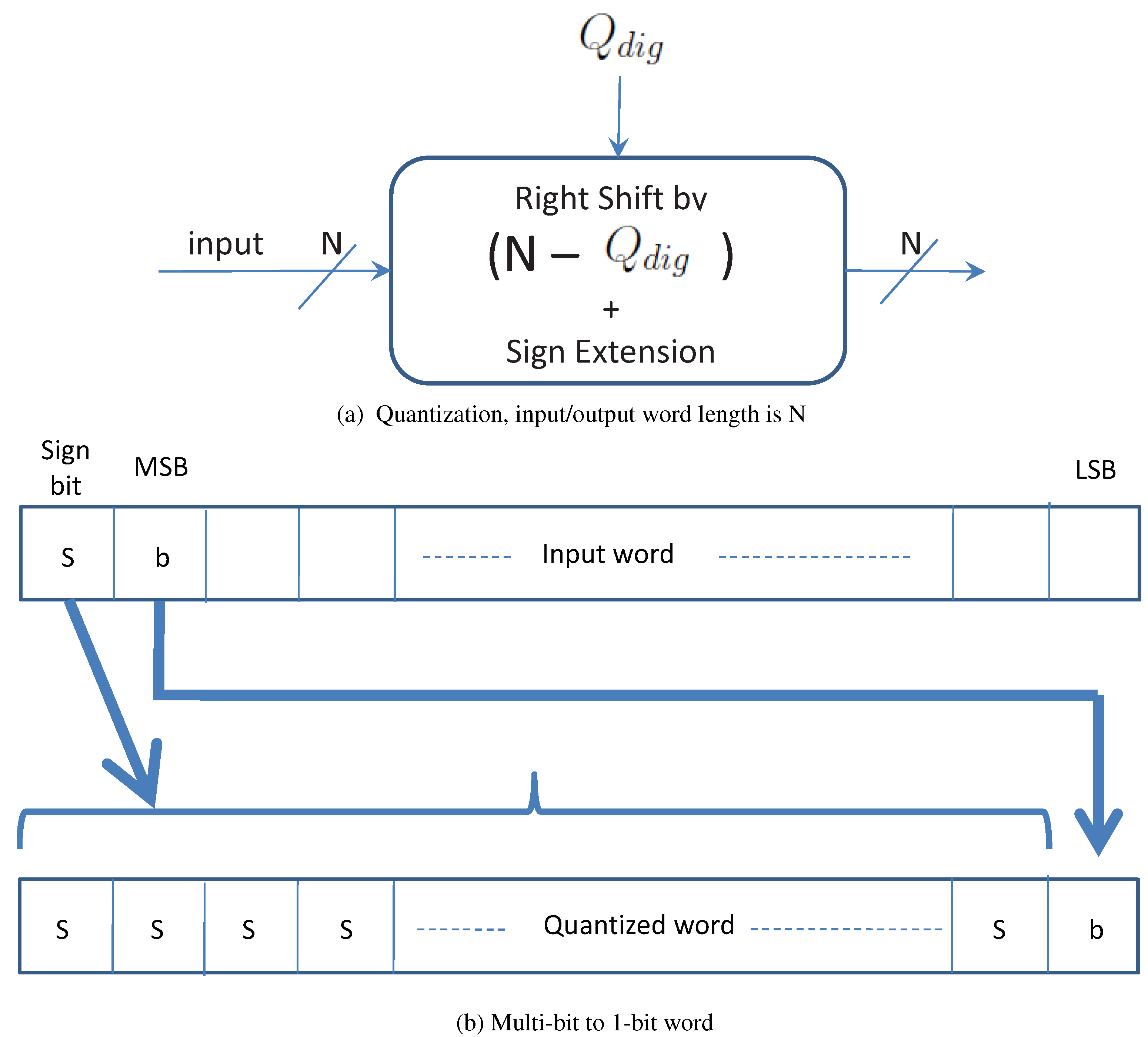
 with sign of the word preserved as shown in Figure 13 for equal to one. By doing this, higher order bits do not see lot of switching when they are processed further in the receiver. There will be activity in the lower order bits of the word. Hence with smaller , there is saving in dynamic power. and combinations for a given
  under different conditions of interference. Case-I corresponds to the case when there is no interference and only noise is present in the system. Case-II corresponds to the case when there is no interference on the alternate channels and only adjacent interference is present with noise. Case-III is the case where adjacent channels are absent, whereas, alternate channels and noise are present in the channel. In case-IV all interferences are present along with noise. Every and combination in the table satisfies the required BER. The estimated power is also shown for all combinations. The combination of and that consumes lowest power for a particular interference and
  condition is put into the LUT. Such entries are listed under gray shading. The power is estimated for maximum length packet. Average power (
  ) is calculated as follows:


 is the average power consumption during preamble and SFD.
  is the average power during data. As shown in Figure 4,
  is preamble and SFD duration. It is symbol long and data is
  symbols long. The power spent during synchronization is fixed ( = mW) and depends on and settings for the data duration. In order to have a simple clock generator, the operating sampling frequency (
  ) for the design are integer division of Msps. They are ,
  , ,
, ,  , , , , and Msps respectively. As shown in Table 1, the sampling frequencies are quantized to the next higher operating sampling frequency. For, e.g., sampling frequency of
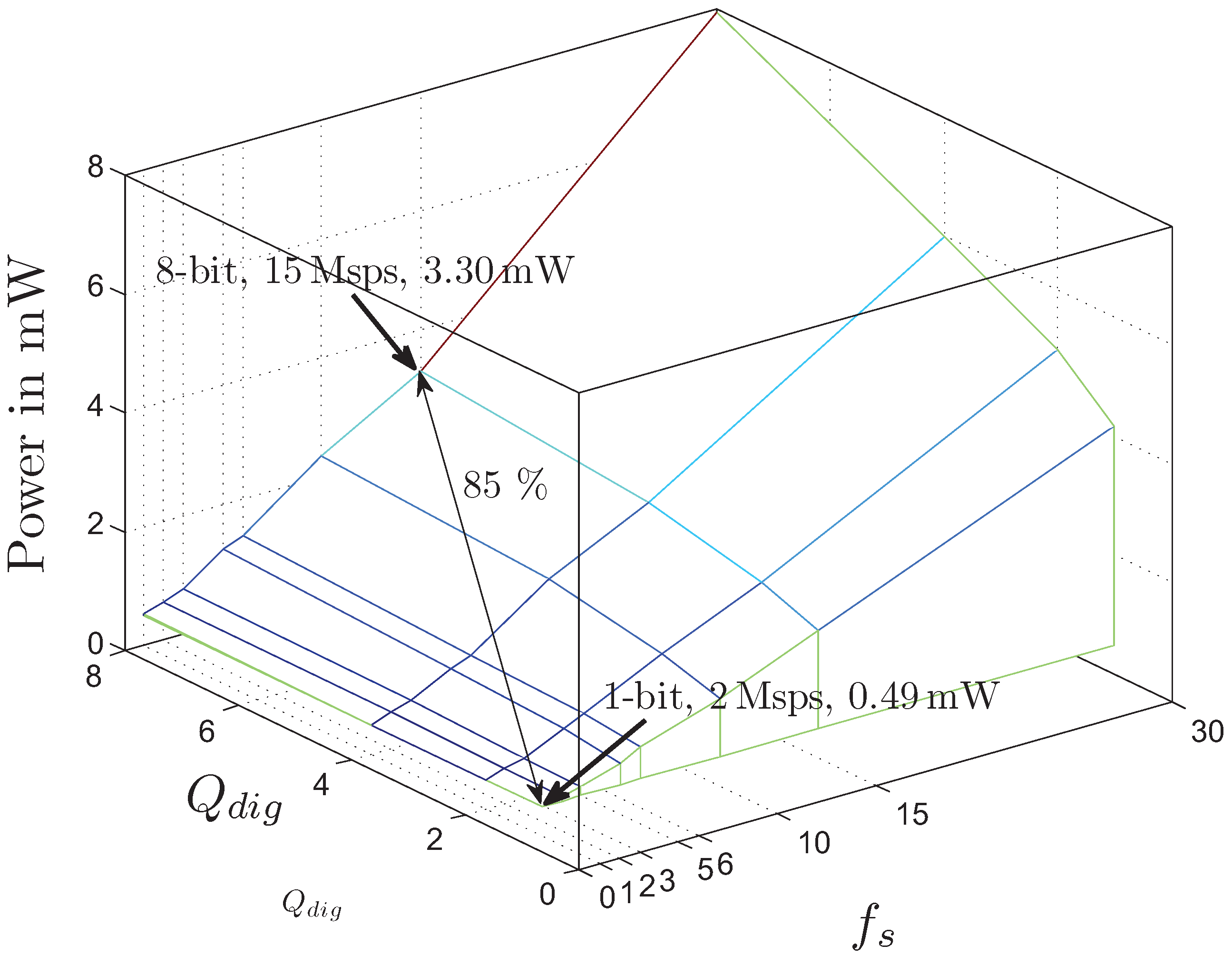
  Msps is raised to Msps. We can see from the table, maximum power consumed by the design is
  mW. The lowest power consumed by the design as can be seen from the table is
  mW, when is Msps and is -bit. At this sampling frequency, there is only one multiplier active in the FIR filter. of 2 Msps means the signal with IF of 3 MHz is under-sampled. In spite of under-sampling and coarsely quantizing ( -bit) the signal, specified BER is achieved when
  is high. Thus we see that saving in power can be approximately seven times when is high and interferences are absent.
 values for the receiver.
| *Interference attenuation | No. of bits
| Sampling Frequency (
/ ) in Msps , Power in mW | ||||||
|---|---|---|---|---|---|---|---|---|
| = dB | =  dB dB | =  dB dB | = dB | = dB | = dB |  dB dB | ||
| Case-I No interference Only noise | 1 | * | 10/10, 1.48 | 7/10, 1.48 | 4/5, 0.85 | 1/1 0.49 | 1/1, 0.49 | 1/1 0.49 |
| 2 | 13/15, 2.49 | 7/10, 1.76 | 4/5, 0.96 | 1/1, 0.49 | 1/1, 0.49 | 1/1, 0.49 | 1/1, 0.49 | |
| 4 | 13/15, 2.92 | 8/10, 2.11 | 1/1, 0.50 | 1/1, 0.50 | 1/1, 0.50 | 1/1, 0.50 | 1/1, 0.50 | |
| 8 | 13/15, 3.30 | 3/3, 0.75 | 1/1, 0.52 | 1/1, 0.52 | 1/1, 0.52 | 1/1, 0.52 | 1/1, 0.52 | |
| Case-II No Alternate Adjacent – Standard Specific | 1 | * | * | * | * | 11/15, 2.5 | 1/1, 0.49 | 1/1, 0.49 |
| 2 | * | * | * | * | 9/10, 1.76 | 1/1, 0.49 | 1/1, 0.49 | |
| 4 | 22/30, 6 | 8/10, 2.11 | 8/10, 2.11 | 7/10, 2.11 | 7/10, 2.11 | 1/1, 0.50 | 1/1, 0.50 | |
| 8 | 12/15, 3.3 | 8/10, 2.7 | 8/10, 2.7 | 7/10, 2.7 | 5/5, 1.23 | 1/1, 0.52 | 1/1, 0.52 | |
| Case-III No Adjacent Alternate – Standard Specific | 1 | * | * | * | 23/30, 4.18 | 9/10, 1.47 | 1/1, 0.49 | 1/1, 0.49 |
| 2 | * | * | 25/30, 5.0 | 19/30, 5.0 | 6/6, 1.5 | 1/1, 0.49 | 1/1, 0.49 | |
| 4 | 13/15, 2.92 | 12/15, 2.92 | 4/5, 1.07 | 4/5, 1.07 | 3/3, 0.71 | 1/1, 0.50 | 1/1, 0.50 | |
| 8 | 14/15, 3.3 | 7/10, 2.7 | 4/5, 1.19 | 4/5, 1.23 | 3/3, 0.75 | 1/1, 0.52 | 1/1, 0.52 | |
| Case-IV Standard Specific | 1 | * | * | * | * | 15/15, 2.15 | 5/5, 0.85 | 1/1, 0.49 |
| 2 | * | * | * | * | 14/15, 2.49 | 3/3, 0.66 | 1/1, 0.49 | |
| 4 | 23/30, 6.0 | 13/15, 2.92 | 13/15, 2.92 | 7/10, 2.11 | 6/6, 1.19 | 1/1, 0.50 | 1/1, 0.50 | |
| 8 | 14/15, 3.3 | 13/15, 3.3 | 7/10, 2.7 | 7/10, 2.7 | 6/6, 1.38 | 1/1, 0.52 | 1/1, 0.52 | |
 will not result in acceptable BER; Cells in gray shade are the ones fed to the LUT in the receiver.
 mW to mW. It suggests that even with a high-order interference reject filter in RF chain of the receiver, just by
  estimation power saving of the order of 5 times is possible. It is evident from the Table 1 that when
  is very high (
  dB), of Msps and of -bit works for all interference condition. Thus inaccuracy in interference detection is tolerable at very high as mentioned in a previous section on IDSE. Since this is the power averaged over the maximum packet length possible, the lowest power values is a function of packet length. The average packet length depends on the application and usage. The power numbers for different packet length can be obtained from Equation (12). One more point to consider while looking at the power numbers is, the numbers do not include the possible power savings that can be obtained from a variable resolution ADC. A variable resolution and variable sampling rate ADC can take advantage of different possible and settings to lower the power consumption.
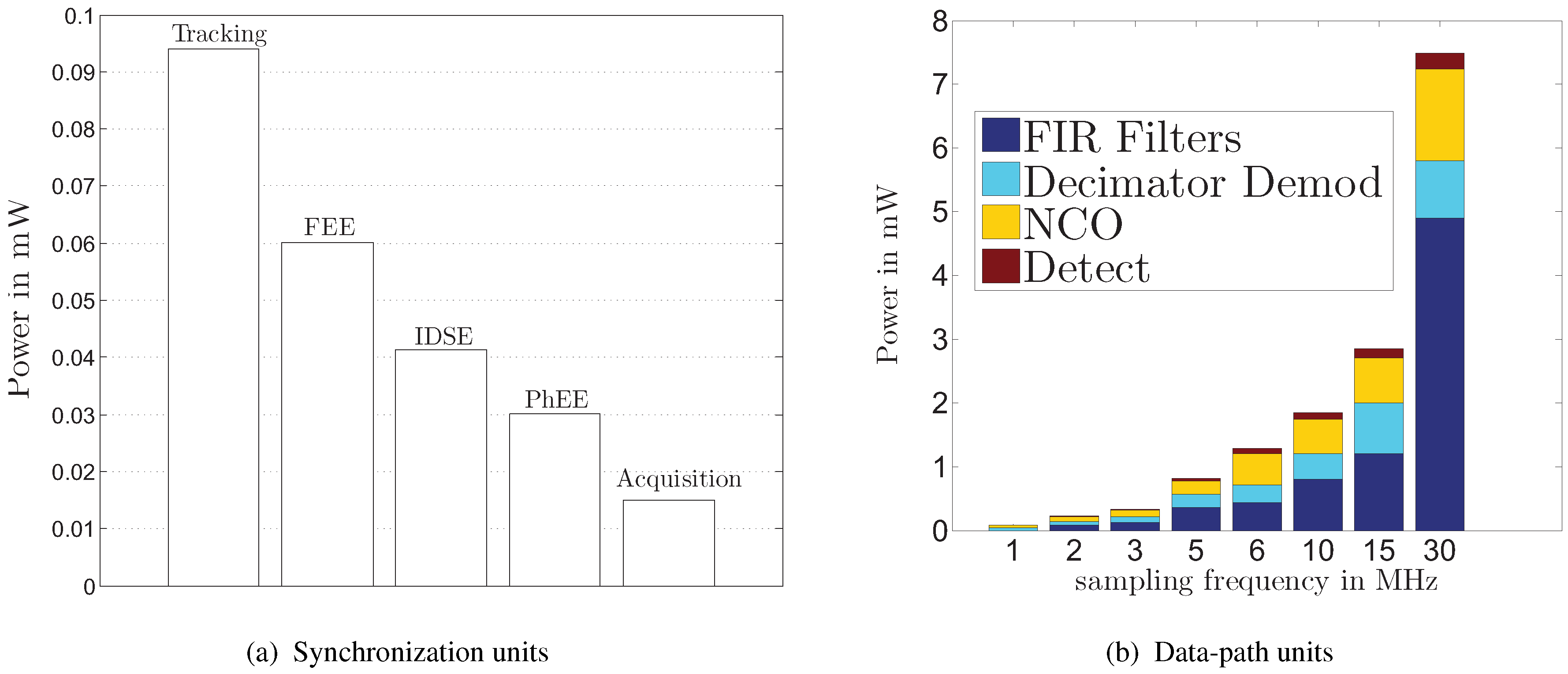
 K gates. We see that tracking unit has largest gate count. We see that expense of adaptivity and lowering power is
  % additional gate count of IDSE unit. The design contains approximately
  % memory elements (ROM). The design has many Baugh–Wooley 2’s complement signed multipliers in it, it is by virtue of many FIR filters in IDSE unit and in data-path. Though synchronization units consume more area as shown in Table 2, average power consumed by synchronization units is very less. Considering this, we realize that adding any component to data-path requires more attention than adding a component to synchronization unit. Finally, Figure 14 shows the power consumption as a function of and , as was discussed while formulating the design problem in Equation (1).
| Blocks and Gate count in % | |||
| IDSE | 16 | Tracking | 36 |
| Match Filters | 19.8 | Acquisition | 5.7 |
| PhEE | 4.95 | Demod | 4.83 |
| ROM | 4.1 | FEE | 4 |
| NCO | 2.4 | Detector | 1. |
| Theta gen. | 0.86 | ||
| Designed for | IEEE 802.15.4-2006 |
| Technology | UMC 130 nm CMOS |
| Gate count | ~606 K gates |
| Area | ~2.42 mm  |
| Power | variable, 0.49–3.3 mW |
| Frequency | variable, 1–30 Msps |
and , Equation (1). Variation in power consumption of the design in seen to be  %.
and , Equation (1). Variation in power consumption of the design in seen to be %.
%.
and , Equation (1). Variation in power consumption of the design in seen to be %.
6. Experimental Results and Discussions
 GHz. Inputs are modulated RF and local oscillator signals. The RF input from signal generator is downconverted to IF and digitized before presenting it to the FPGA board. The FPGA does the further processing in the digital to extract the packet. Packet error and packet loss are measured inside the FPGA. This is done by transmitting a packet with 20 known symbols by triggering the VSG repeatedly. Demodulated symbols are compared with the stored sequence of symbols in the FPGA. The packet error counter (packet_err_count) is incremented with every packet error. For packet loss measurement, number of packet transmitted is counted and compared with the number of sync_succ occurred, i.e., number of time synchronization is achieved.
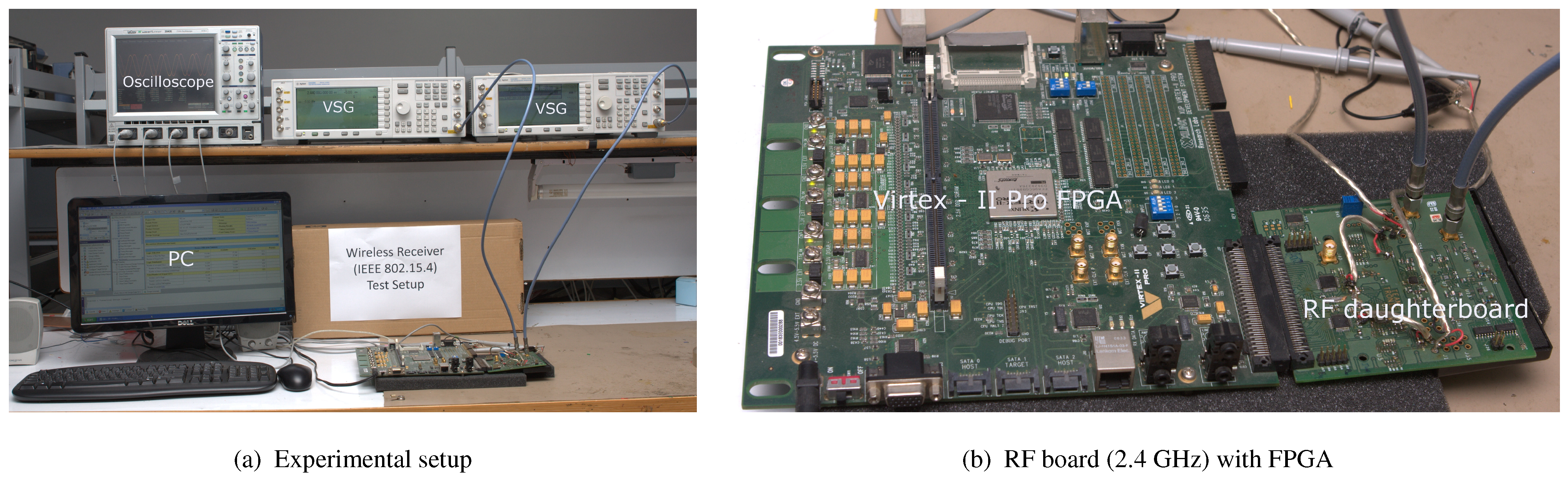
 -bit and the clock frequency is Msps. The power consumption of the receiver is less when the receiver processes such low resolution (time and amplitude) signal.
 equal to 8-bit. As can be seen that power consumption by the synchronization unit is much smaller than the units in the data path as they are “ON” for much shorter duration. Among the synchronization units, the fine time tracking unit consumes the most power as it contains many correlators for estimating the fine timing. In data path FIR filters consume the largest power due to many multiply and accumulate units in it. = 8 bit.
= 8 bit.
equal to 8-bit. As can be seen that power consumption by the synchronization unit is much smaller than the units in the data path as they are “ON” for much shorter duration. Among the synchronization units, the fine time tracking unit consumes the most power as it contains many correlators for estimating the fine timing. In data path FIR filters consume the largest power due to many multiply and accumulate units in it. = 8 bit.
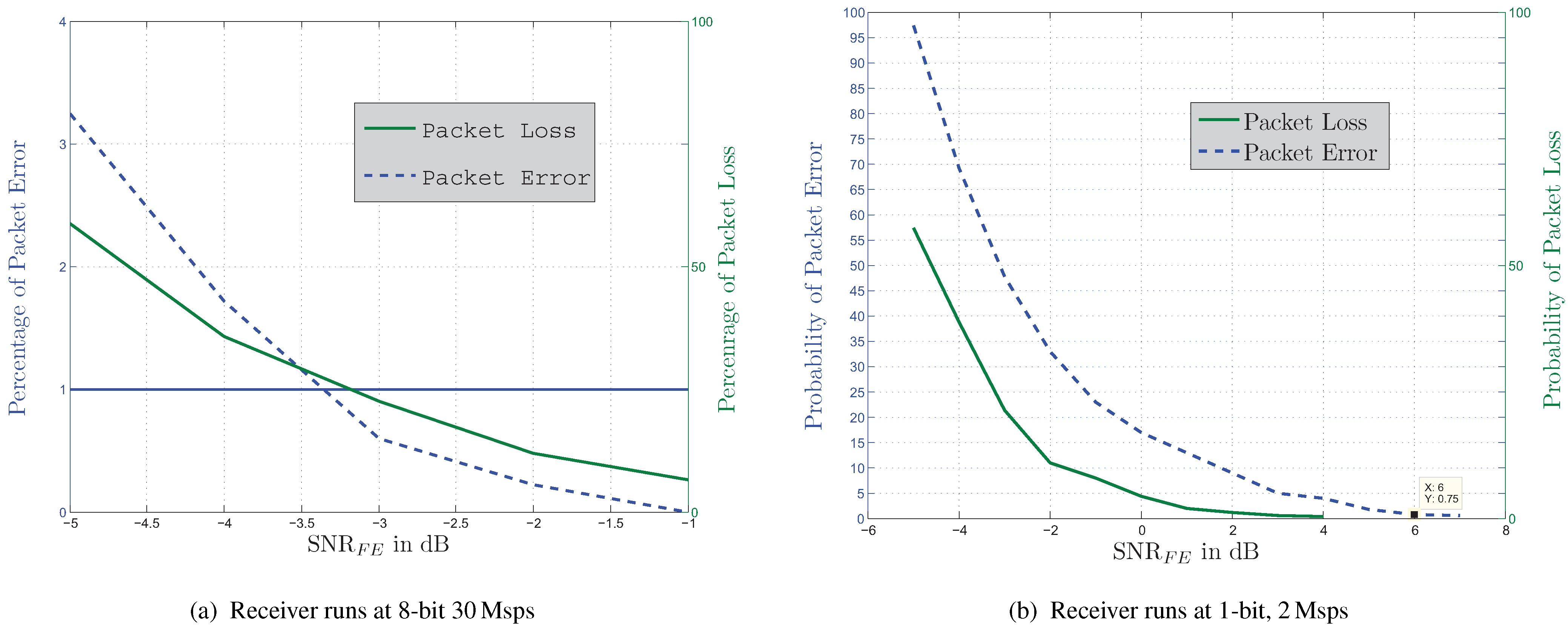
= 8 bit. for the receiver working at -bit and Msps. From the figure it is seen that the required to meet 1% packet error is around
 dB. Whereas, from Table 1 it is seen that the minimum required is around dB. As discussed earlier, non-idealities of the RF front end and the experimental setup might be the reason for this difference. when receiver works on its lowest configuration, -bit and Msps. It is seen from this figure that the lowest meeting the error criteria is around dB. Table 1 suggests that it requires around 5 dB of for -bit Msps setting to meet the error specification. The difference can be attributed to the factors discussed above. The packet loss is nearly same in both Figure 19(a) and Figure 19(b). This is because the synchronization section in both cases runs at same settings of and . Though the experimental values differ from the values obtained through simulation, the difference is not very significant from the point of verifying the idea of the power scalable receiver. The experimental results verify the claim that for different signal conditions different setting ( , ) of the receiver can be used to minimize power while meeting the error criteria. The design of the receiver proves to be working well to receive the packets with different and settings. for two different cases.
7. Conclusions
) and word length ( ) based on interference detection and signal quality ( ) estimation. The approach is based on a LUT in the digital section of the receiver. Interference detector and estimator that suit this approach have been proposed. Settings of different sections of digital receiver changes as and vary. But, this change in settings ensures that the desired BER is achieved. Overall, the receiver reduces amount of processing when conditions are benign and does more processing when conditions are not favorable. A hardware protocol is proposed for packet based communication that facilitates power scalable design. It is shown that the power consumption by the digital baseband can be reduced by % (  times) when there is no interference and ( ) is high. Design is experimentally verified and the proposed fact is established that energy condition of the hardware can be minimized when the signal condition is better.
Acknowledgements
References
- Ludwig, J.T.; Nawab, S.H.; Chandrakasan, A.P. Low-Power Digital Filtering Using Approximate Processing. IEEE J. Solid State Circuits 1996, 31, 395–400. [Google Scholar] [CrossRef]
- Hellmark, L.M. Method and apparatus for adaptive bit resolution in a digital receiver and digital transmitter. U.S. Patent 6504863 B1, 7 January 2003. [Google Scholar]
- Amiri, K.; Cavallaro, J.R.; Dick, C.; Rao, R.M. A High Throughput Congurable SDR Detector for Multi-user MIMO Wireless Systems. J. Signal Process. Syst. 2010, 62, 233–245. [Google Scholar]
- Sinha, A.; Chandrakasan, A.P. Energy Efficient Filtering Using Adaptive Precision and Variable Voltage. In Proceedings of the 12th Annual IEEE International ASIC/SOC Conference, Washington, DC, USA, 15–18 September 1999; pp. 327–331.
- Haykin, S. Adaptive Filter Theory; Prentice Hall: Upper Saddle River, NJ, USA, 2002. [Google Scholar]
- Bougard, B.; Catthoor, F.; Daly, D.C.; Chandrakasan, A.; Dehaene, W. Energy Efficiency of the IEEE 802.15.4 Standard in Dense Wireless Microsensor Networks: Modeling and Improvement Perspectives. In Proceedings of the DesignAutomation and Test in Europe, Munich, Germany, 7–11 March 2005; pp. 196–201.
- Kluge, W.; Poegel, F.; Roller, H.; Lange, M.; Ferchland, T.; Dathe, L.; Eggert, D. A fully integrated 2.4-GHz IEEE 802.15. 4-compliant transceiver for ZigBee applications. IEEE J. Solid State Circuits 2006, 41, 2767–2775. [Google Scholar] [CrossRef]
- Tedeschi, M.; Liscidini, A.; Castello, R. Low-Power Quadrature Receivers for ZigBee (IEEE 802.15. 4) Applications. IEEE J. Solid State Circuits 2010, 45, 1710–1719. [Google Scholar] [CrossRef]
- Troesch, F.; Steiner, C.; Zasowski, T.; Burger, T.; Wittneben, A. Hardware Aware Optimization of an Ultra Low Power UWB Communication System. In Proceedings of the 2007 IEEE International Conference on Ultra-Wideband (ICUWB 2007), Singapore, 24–26 September 2007; pp. 174–179.
- Retz, G.; Shanan, H.; Mulvaney, K.; O’Mahony, S.; Chanca, M.; Crowley, P.; Billon, C.; Khan, K.; Quinlan, P. A Highly Integrated Low-Power 2.4 GHz Transceiver Using a Direct-Conversion Diversity Receiver in 0.18
![Jlpea 02 00242 i008]() m CMOS for IEEE 802.15.4 WPAN. In Proceedings of the 2009 IEEE International Solid-State Circuits ConferenceDigest of Technical Papers (ISSCC 2009), San Francisco, CA, USA, 8–12 February 2009; pp. 414–415, 415a.
m CMOS for IEEE 802.15.4 WPAN. In Proceedings of the 2009 IEEE International Solid-State Circuits ConferenceDigest of Technical Papers (ISSCC 2009), San Francisco, CA, USA, 8–12 February 2009; pp. 414–415, 415a. - Oh, N.J.; Lee, S.G. Building a 2.4 GHz Radio Transceiver using 802.15.4. IEEE Circuits Dev. Mag. 2005, 21, 43–51. [Google Scholar] [CrossRef]
- Viterbi, A.J. CDMA Principles of Spread Spectrum Communication; Addison-Wesley Longman, Inc.: Boston, MA, USA, 1995. [Google Scholar]
- Meyr, H.; Moeneclaey, M.; Fechtel, S. Digital Communication Receivers: Synchronization, Channel Estimation, and Signal Processing; John Wiley & Sons, Inc.: New York, NY, USA, 1997. [Google Scholar]
- Ammer, M.J. Low Power Synchronization for Wireless Communication. Ph.D. Thesis, University of California Berkeley, Berkeley, CA, USA, 2004. [Google Scholar]
- IEEE Std 802.15.4-2006. IEEE Standard for Information Technology–Local and Metropolitan Area Networks–Specific Requirements–Part 15.4: Wireless Medium Access Control (MAC) and Physical Layer (PHY) Specifications for Low-Rate Wireless Personal Area Networks (LR-WPANs). Available online: http://ieeexplore.ieee.org/servlet/opac?punumber=11161 (accessed on 16 October 2012).
- Scolari, N.; Enz, C.C. Digital receiver architectures for the IEEE 802.15.4 standard. In Proceedings of the 2004 International Symposium on Circuits and Systems (ISCAS ’04), Vancouver, Canada, 23–26 May 2004; pp. 345–348.
- Jeruchim, M. Techniques for Estimating the Bit Error Rate in the Simulation of Digital Communication Systems. IEEE J. Sel. Areas Commun. 1984, 2, 153–170. [Google Scholar] [CrossRef]
- Yee, D.G.W. A Design Methodology for Highly-Integrated Low-Power Receivers for Wireless Communications. Ph.D. Thesis, University of California Berkeley, Berkeley, CA, USA, 2001. [Google Scholar]
- Cho, K.M. Optimum gain control for A/D conversion using digitizing I/Q data in quadrature sampling. IEEE Trans. Aerosp. Electron. Syst. 1991, 27, 178–181. [Google Scholar] [CrossRef]
- Do, A.V.; Boon, C.C.; Anh, M.; Yeo, K.S.; Cabuk, A. An Energy Aware CMOS Receiver Front end for Low Power 2.4 GHz Applications. IEEE Trans. Circuits Syst.I 2010, 57, 2675–2684. [Google Scholar] [CrossRef]
- Andraka, R. A survey of CORDIC algorithms for FPGA based computers. In Proceedings of the 1998 ACM/SIGDA Sixth International Symposium on Field Programmable Gate Arrays (FPGA ’98), Monterey, CA, USA, 22–24 February 1998; ACM Press: New York, NY, USA, 1998; pp. 191–200. [Google Scholar]
- Vankka, J. Direct Digital Synthesizers: Theory, Design and Applications. Ph.D. Thesis, Helsinki University of Technology, Helsinki, Finland, 2000. [Google Scholar]
- Xilinx, Inc. Xilinx Virtex II Pro Boards. 2010. Available online: http://www.xilinx.com/univ/xupv2p.html (accessed on 1 December 2010).
© 2012 by the authors; licensee MDPI, Basel, Switzerland. This article is an open-access article distributed under the terms and conditions of the Creative Commons Attribution license ( http://creativecommons.org/licenses/by/3.0/).
Share and Cite
Dwivedi, S.; Amrutur, B.; Bhat, N. Power Scalable Radio Receiver Design Based on Signal and Interference Condition. J. Low Power Electron. Appl. 2012, 2, 242-264. https://doi.org/10.3390/jlpea2040242
Dwivedi S, Amrutur B, Bhat N. Power Scalable Radio Receiver Design Based on Signal and Interference Condition. Journal of Low Power Electronics and Applications. 2012; 2(4):242-264. https://doi.org/10.3390/jlpea2040242
Chicago/Turabian StyleDwivedi, Satyam, Bharadwaj Amrutur, and Navakanta Bhat. 2012. "Power Scalable Radio Receiver Design Based on Signal and Interference Condition" Journal of Low Power Electronics and Applications 2, no. 4: 242-264. https://doi.org/10.3390/jlpea2040242