1. Introduction
While power reduction is commonly achieved through technology scaling and aggressive supply voltage reduction [
1–
4]; these methods affect the output swing of the sensor and thus decrease its dynamic range (DR), as expressed in
(1).
where
Cpd represents the photodiode capacitance, upon which the charge is integrated;
Vmax and
tmin represent the pixel swing and the minimal available integration time;
imax and
imin represent the maximum and minimum currents that can be detected by the sensor.
The narrow DR of image sensors causes the saturation of a pixel with high sensitivity, in the case of high illumination levels, resulting in a partial loss of information. Insufficient DR of conventional video cameras is a one of the key problems in realizing a robust vision system for capturing images consisting of wide illumination conditions within the same scene.
Various solutions for extending the DR in CMOS Image Sensors (CISs) have been presented in recent years. WDR algorithms can be divided into seven general categories that were thoroughly compared in [
5]: (1)
Logarithmic Sensors that compress their response to light due to their logarithmic transfer function [
6,
7]; (2)
Multimode Sensors that have a linear response at dark illumination levels and a logarithmic response at bright illumination levels (
i.e., they are able to switch between linear and logarithmic modes of operation) [
8]; (3)
Clipping Sensors, in which a capacity well adjustment method is applied [
9,
10]; (4)
Frequency-Based Sensors, where the sensor output is converted into a pulse frequency [
11,
12]; (5)
Time-to-First Spike (TFS) Sensors, where the image is processed according to the time the pixel was detected as saturated [
13,
14]; (6) sensors with
Global Control over the integration time [
15–
17]; and (7) sensors with
Autonomous Control over the integration time, where each pixel has control over its own exposure period [
18–
25].
Our group has designed three generations of WDR imagers which are based on the autonomous control over integration time method. All generations of the aforementioned sensors were based on our proposed multiple resets WDR algorithm. According to this algorithm, the full integration time for the frame is subdivided into
NWDR intervals, preferably in a sequence of progressively shorter intervals, according to the down-going series:
where
X is a chosen constant (
X >1), such as 2, and
TINT represents the full integration time.
NWDRrepresents the number of bits, by which the pixel DR is extended. A typical range of values for
NWDR when
X equals 2, is 4–8; thus the DR is extended by 24 and 48 dB, respectively.
At the end of each interval, a non-destructive readout of the pixels is performed, and the readout level of each pixel is compared to a respective threshold. Based on the comparison result, it is determined if the pixel will saturate before the end of the frame. If it is determined that the pixel will saturate, the pixel is reset. Consequently, the reset operation is conditional and is applied individually to each pixel depending on its output at the saturation checkpoints. Thus, each pixel autonomously adjusts its integration time. Resetting the pixel at an intermediate point during the integration period significantly reduces the probability that the pixel will saturate prior to the final readout. The binary information that shows if the reset was applied or not is saved in a digital storage in order to enable proper scaling of the value read. The incident light intensity is then calculated at the end of the integration period by multiplying the final readout level by a scaling factor which is based on the length of time since the last reset. This length of time can be determined according to the number of times the given pixel was reset over the entire integration period. Therefore, the light intensity of the pixel is calculated as:
where
Value is the final value that describes the incident light intensity;
Man (Mantissa) is the analog or digitized output value that is read out at the end of the integration period; and
EXP (Exponent) is the number of times the given pixel was reset over the entire integration period.
The first of these imagers, presented in 2003, was implemented in 0.5 μm technology and was able operated in a rolling shutter mode. Characterized by a very simple pixel structure with a 14.4 μm × 14.4 μm size and consisting of 4 in-pixel NMOS transistors, this imager was operated with a 5 V power supply and provided a DR extension of up to 12 dB [
18]. The sensor provided a high fill factor and a small in-pixel transistor count, since all processing circuits required for WDR algorithm realization were implemented at the array periphery, without penalizing the imager's spatial resolution. The second imager, initially presented in 2005, was fabricated in a 0.35 μm process and could be operated in both rolling and global shutter operating modes [
21]. Since operation in the global shutter mode required parallel reset and integration of all pixels in the sensor array, this imager required in-pixel processing circuitry. As a result, each pixel had an 18 μm × 18 μm size, consisted of 11 NMOS and 8 PMOS transistors and provided a fill factor of 15%. The parallel operation of all pixels in the array resulted in increased peak power dissipation, requiring utilization of advanced design methods for power reduction. The image sensor was operated by dual power supplies (1.8 V and 1.2 V) and provided DR extension of up to 48 dB [
21]. In the third imager, presented in 2007, we successfully combined the concepts that were used in the first and the second sensors. This imager was implemented in a 0.18 μm process, with a pixel size of 7 μm × 7 μm, a fill factor of more than 20%, and both rolling and global shutter capabilities. This was achieved by implementing most of processing circuits at the array periphery. The sensor used a 1.8 V power supply and was expected to provide a DR extension of up to 48 dB [
23].
This paper briefly reviews the designs of the aforementioned sensors. A comprehensive analysis of the power-performance tradeoffs of all imagers is discussed based on simulation results carried out in a 0.18 μm standard CMOS process. The performed simulations, which mimic the operation of the fabricated imagers, provide us with a qualitative assessment of the currents, voltages, and power developing within various blocks of the imagers during their operation. Utilizing the data from the aforementioned simulations, we are able to assess the influence of various design parameters, such as supply voltage, number of WDR extension bits,
etc., on the power dissipation of each of the sensors. We also analyze the relative part of the total power dissipation of the different blocks within the sensor. The temporal power dissipation profile is presented and explained with reference to the features of each of three WDR imagers. We show the connection between the power dissipation characteristics of each sensor and its image quality. By analyzing the tradeoffs that exist between the image quality and the power, we conclude which of the presented sensors [
18,
21,
23] exploits the consumed power with highest effectiveness.
The rest of this paper is constructed as follows: Section 2 presents a detailed description of the operation of the three imagers; Section 3 presents the power-performance tradeoffs analysis and discusses the simulated and calculated results; Section 4 summarizes the results and concludes the paper.
2. Three Generations of WDR Solutions
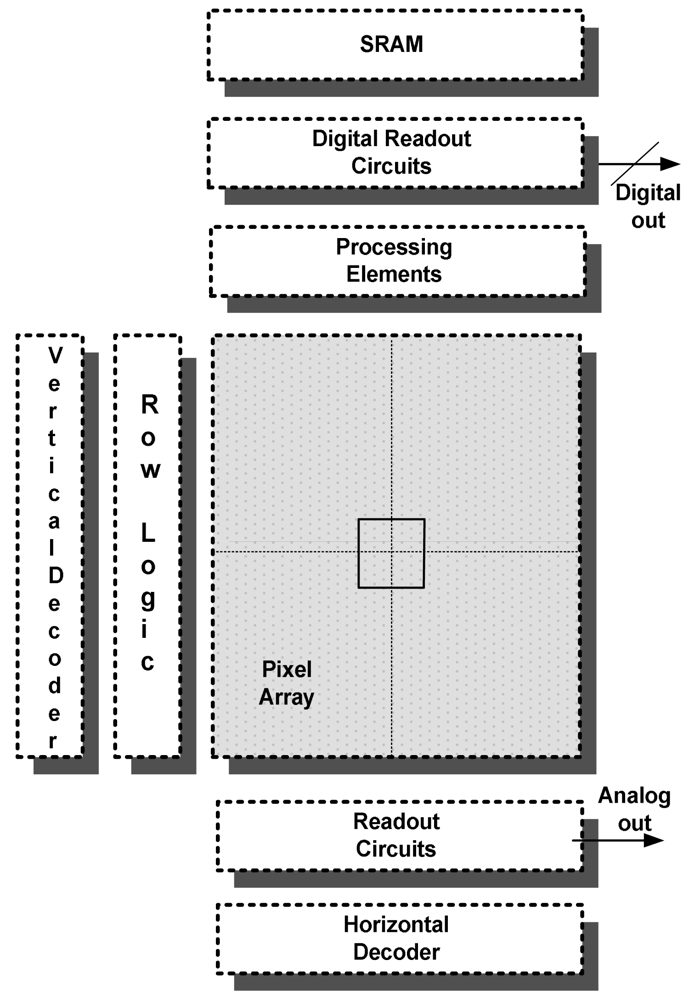
The general architecture of all the presented imagers is similar and is shown in
Figure 1. The sensor consists of a pixel array; a single vertical (row) decoder; row logic; a single horizontal (column) decoder; analog readout circuitry processing elements; digital readout circuits; and an SRAM. All the designs make use of column parallel architectures to share the processing circuits among the pixels in a column. Integration time can be adjusted for each pixel with this architecture, and non-destructive readout of the pixel can be performed at any time during the integration period by reading the voltage on the column bus.
Although the imagers employ similar algorithms, their operation, pixels, timing, and decision circuitry structures are different. The following sub-sections provide more detailed descriptions of these sensors.
2.1. First Generation—0.5 μm WDR Sensor with Rolling Shutter Operation
The first sensor [
18] operates in rolling shutter mode, where the integration between the different rows starts with a certain skew. As in a traditional rolling shutter Active Pixel Sensor (APS), our imager is constructed of a two-dimensional (2-D) pixel array, with random pixel access capability (
Figure 1). The described imager is comprised of 64 rows and 64 columns.
The random access capability is achieved through
Vertical and
Horizontal Decoders. The reset and other pixel operations are delivered by the
Row Logic block. The saturation checks for extending the DR are performed within the
Processing Circuits at the upper part of the chip. The binary results of the saturation checks are stored in the SRAM block. The readout circuits of digital information regarding the saturation are located within the
Digital Readout Circuits block. The readout of the pixel's analog values (Mantissa) is performed by the
Analog Readout Circuits. After the integration of the induced photo-current ends for a certain row, the pixels of that row are readout to an Analog-to-Digital Converter (ADC), which is located outside of the chip. At the same time, the digital information associated with that row is retrieved from the SRAM. The final pixel value is calculated according to the floating point representation, as was shown in
Equation (3) above.
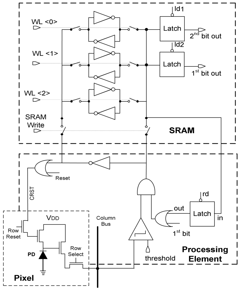
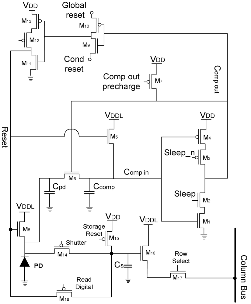
Figure 2 shows the implementation of a single pixel along with its processing element and SRAM (shared by all pixels in a column). Each individual pixel contains a photodiode (
PD) for light measurement; a reset input; a conditional reset control; and an electrical output representing the measured illumination. Each pixel contains an additional transistor, in series with the row reset transistor, activated by a vertical column reset signal that enables of independent reset of the pixel.
In this way, the integration time can be adjusted for each pixel, and non-destructive readout of the pixel can be performed at any time during the integration period. This is done by activating the row select transistor and reading the voltage on the column bus.
The Processing Element contains the saturation detection and the decision logic circuit, and it is shared by all pixels in a column. Because of this column parallel architecture, the pixel array contains a minimum amount of additional circuitry and there is little sacrifice in fill factor.
If the pixel discharges below the threshold, the pixel is detected as saturated. This information and the binary information concerning the previous saturation check (stored in the memory), are ANDed to make a decision whether to reset the pixel or not. If the current saturation check is the first one within the frame, a logic signal 1st bit is raised, and a logic “1” is loaded into the Processing Element's latch. If the decision is positive, the column reset (CRST) and the Row Reset lines must both be precharged to a logical high voltage to activate the reset transistor, and the photodiode restarts integration. When the decision is negative, the reset is not activated and the pixel continues to integrate. The binary information, on whether the reset was applied or not, is saved in the SRAM storage and is output to the latches in due time. Once the row is readout through the regular output chain, this additional information is retrieved from the memory through the latches.
The design described above was fabricated in silicon and successfully tested. The sensor achieved 2 bits of DR enhancement. This concept supported only rolling shutter operation, and was not capable of capturing fast changing scenes.
Table 1 shows the attributes of the fabricated chip, as presented in [
18].
2.2. Second Generation—0.35 μm WDR Sensors with Global Shutter Capability
The solution to minimizing the image distortion in scenes with fast moving objects is to operate the sensor in a global shutter (snapshot) mode, in which the integration of all pixel rows array starts simultaneously without any skew. A WDR snapshot CMOS sensor was presented in [
21].
The general architecture of the sensor, proposed in that work, is similar to the previous implementation [
18]. The functionality of all the blocks except the pixel array was not changed. However, a completely different pixel structure was designed to suit the snapshot operation.
Figure 3 shows the scheme of a single pixel. The presented circuit operates as follows: at the beginning of the frame the pixel is reset by applying “0” to the conditional (
Cond Reset) and
Global Reset signals. Therefore, the internal “
Reset” node is equal to “1 h” (1.8 V) independent of the value of “
Comp out”, thus charging the photodiode capacitance
Cpd and
Comp_in capacitance
Ccomp, to the value of the lower supply voltage
VDDL, provided that the following relation holds:
where
VDD is the higher supply voltage, which equals 1.8 V (“1 h”) and
VthN is the threshold voltage of the NMOS transistors implementing the pixel functionality. This threshold voltage is approximately 0.6 V. Therefore, according to
(4), the lower limit on
VDDL equals 1.2 V (“1”). At the same time, the internal line
Comp out is precharged to 1.8 V by negative pulse
Comp out pre-charge = “0”. The reset phase is stopped by applying “1” to the
Cond Reset and
Global Reset signals and the photodiode starts discharging, according to the energy of the impinging light. At this stage, the total capacitance connected to the photodiode is given by:
At the end of the first integration interval the output of the photodiode (voltage on C′pd) is compared with an appropriate threshold, associated with the switching threshold voltage of the comparator, implemented by a conventional inverter. This comparison is performed by enabling the inverter operation by pulsing the Sleep and the Sleep_n signals high and low, respectively.
If the pixel discharges below the comparator threshold (meaning that the pixel will saturate at the end of the integration time), Comp out becomes “1 h”. At the same time, Cond Reset falls to “0” by applying a short negative pulse, causing M9 and M10 to operate as a standard inverter and enabling operation of the inverter, consisting of M11, M12 and M13. As a result of that inverter operation, the photodiode is reset again. The binary information that shows if a reset was applied or not is locally saved in the storage capacitor CS by pulsing Read Digital to “0”. Afterwards, this binary information is transmitted to the external digital storage associated with the pixel in the upper part of the sensor array, in order to enable proper scaling of the value read. Note that the digital information is readout through a standard Source Follower (SF), composed of M16 and M17, by activating the Row Select signal.
If the pixel is not detected as saturated, Comp out is low and the Reset line remains low, such that the pixel is not reset and continues to integrate untouched until the next frame. Once Comp out becomes low, M6 completely disconnects the photodiode from the comparator. Thus, the comparator input capacitance does not discharge with the photodiode and each subsequent comparison generates a logical “0” until the next frame. After the final saturation check Comp out pre-charge is pulsed low and M6 forms the C′pd capacitance once again, such that no charge is lost during the integration regardless of the comparisons results.
During the next stage, the charge that is accumulated in C′pd is transferred to a storage capacitor Cs, by applying “1 h” to the Shutter switch. Before this charge transfer, the storage capacitor is reset to “1 h” by pulsing the Storage Reset switch low. Once this charge transfer has been completed, the photodiode is able to begin a new frame exposure, and the charge that was just transferred to the in-pixel memory is held there until it is read out at its assigned time in a row-by-row readout sequence through the output chain.
Since each pixel comprises a comparator, which can switch simultaneously throughout the whole array, and logic, which decodes the reset operation, several power and area reduction techniques were utilized to decrease the implementation cost. The area is reduced by implementing the Mux (
Figure 3), with
Pass Transistor Logic (PTL) and
Gate Diffusion Input (GDI) design techniques. The power was reduced by leakage current control in the analog and digital circuits. Differentiation between the “active” and “sleep” modes of each circuit by insertion of a “sleep” transistor was applied to the in-pixel circuits, such as the Mux and comparator. Similarly to the digital circuits, which utilize the dual supply voltage approach, the designed sensor used a high (1.8 V) supply in all critical paths, while low-voltage supply (1.2 V) was applied in others.
The sensor was successfully tested and provided an 8 bit WDR extension, while consuming only 24–29 nW per pixel [
22]. Nevertheless, the resulting global shutter pixel occupied a relatively large area.
Table 2 shows the attributes of the fabricated chip, as presented in [
22].
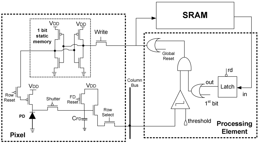
2.3. Third Generation—0.18 μm WDR Sensors with Global Shutter Capability
Another snapshot sensor was proposed in [
23]. The system architecture of the presented sensor is similar to the previous two WDR solutions. The pixel was modified as depicted in
Figure 4.
The presented circuit operates as follows: at the beginning of the frame the photodiode capacitance is reset by applying “1” to Global Reset, pulsing the Write signal high and pulsing the Row Reset signal low. The Shutter switch is off during the reset period.
At the end of the reset Row Reset becomes “1” and the photodiode starts integrating the photo-generated charge. Before reaching the time at which the first row of pixels starts comparison, the parasitic floating diffusion capacitor CFD is pre-charged using the FD_Reset switch. Once the precharge is completed, the Shutter switch is switched on, enabling charge transfer between the photodiode capacitance and floating diffusion capacitance
At certain time points the pixels are scanned row by row to the column-wise comparators. If the current saturation check is the first one within the ongoing frame, then the 1st bit signal is raised.
Otherwise, the digital data regarding the previous check is loaded from the SRAM to the latch that is inside the
Processing Element (
Figure 4). If the pixel is detected as saturated, both the in-pixel static memory cell and the external SRAM cell associated with that pixel are loaded with a logic “1”; Otherwise the memory cells are loaded with “0”. The saturation checks of the different rows are skewed; however, providing that the time to produce of a single WDR bit for every row is short enough, the threshold, in respect to which the pixels are compared, can remain constant. After all the rows were scanned and the in-pixel memories were loaded with the binary reset decisions,
Row Reset is applied globally to the whole array. Each pixel is individually reset or not according to the 1-bit data stored in the in-pixel memory cell.
At the end of the frame the Shutter switch disconnects the photodiode and the floating diffusion capacitances. The photodiode starts a new exposure, whereas the floating diffusion capacitance holds the mantissa from the previous frame until it is read out. The digital information is extracted from the upper part of the chip simultaneously with the analog value readout.
The presented snapshot pixel occupies less area than the one presented in [
21,
22] due to locating the processing circuits outside of the pixel.
Table 3 summarizes the attributes of the fabricated imager.
3. Power-Performance Tradeoffs Analysis
In order to perform a comprehensive qualitative analysis of the power-performance tradeoffs we present a set of assumptions, according to which all the described WDR imagers were simulated. The first assumption is that we concentrate only on the core circuitry of the imagers. The core of each WDR imager consists of a pixel array, the row logic, processing circuits, and digital and analog output chains. Other blocks, such as SRAM and ADCs, are not analyzed, since they have the same structure and power profile for all WDR solutions. In order to provide fair comparisons, the core circuitries of all imagers were implemented in the same 0.18 μm standard CMOS technology and simulated using Cadence Spectre simulator. The Spectre simulator is a very accurate tool for testing the performance of integrated circuits. It is capable of performing DC, AC and transient simulations. This simulator analyzes the integrated circuit according to BSIM3 algorithm.
The first and third generations (1G and 3G) sensors, presented in [
18] and [
23], utilize a single supply voltage
VDD, which typically equals 1.8 V. The second generation (2G) sensor, presented in [
21], employs the dual supply voltage approach. The higher supply voltage (
VDD) equals 1.8 V, whereas the lower one,
VDDL, equals 1.2 V (
Table 4).
All three WDR systems were simulated with the same pixel array size of 480 rows × 640 columns. In addition, the pixels of all three WDR arrays employ photodiodes with the same structure and size, and therefore they present an equivalent photodiode capacitance,
Cpd. Therefore, the total area of each of the pixels directly depends on the in-pixel transistor count, as shown in
Table 4.
The conversion gain, which transforms the integrated photo-charge into the voltage at the in-pixel amplifier input (SF), differs from rolling to global shutter pixels. In the rolling shutter pixel, the conversion gain is inversely proportional to the photodiode capacitance, whereas in the global shutter pixels it is inversely proportional to the floating diffusion capacitance. In the 2G and 3G pixels, the floating diffusion capacitances equal CS and CFD, respectively.
One of the important Figures of Merit (FOM) is the maximal output swing of the pixel. This FOM differs between the three systems, according to the pixel structure of each system. The maximum output signal is set by the reset circuitry and by the SF that are implemented inside the pixels. In the 1G solution, there are two NMOS transistors that implement the conditional reset function (
Figure 2). Therefore, the reset level of the photodiode is two threshold voltages lower than
VDD. During readout, an additional threshold voltage drop occurs, such that the maximum output signal,
Spix1, is given by:
where
VthN is the threshold voltage of the NMOS transistor (0.45 V).
The maximal pixel swing in the 2G sensor is improved, due to the employment of the dual supply approach (
Figure 3). The photodiode is initially reset to
VDDL. During readout, similarly to the 1G sensor, an additional threshold voltage drop occurs. Therefore the output swing,
Spix2, is given by:
The pixel swing is maximized in the 3G sensor, since the photodiode is reset to
VDD through the conditional reset scheme that is implemented with two PMOS transistors (
Figure 4). The SF utilized in this pixel is similar to the ones implemented in the previous two solutions. Consequently, the maximal swing,
Spix3, equals:
Since all of the pixels comprise the same NMOS transistors, the influence of process corners on the maximal pixel swings (Spix1, Spix2, Spix3) is similar. In all presented simulations, the default number of WDR bits (NWDR) is 4; however, the influence of extending this value is also examined and analyzed. All the analyzed sensors are operated at the same frame rate of 33 frames per second (fps).
Table 5 presents the simulated average
Power per Pixel (PPX) for the imagers at different corners and temperatures. Generally, the
Slow-Slow (SS) corner results in a minimal PPX, whereas the
Fast-Fast (FF) corner results in a maximal PPX. This can be explained by the gradual decrease of the threshold voltage of MOS transistors in the
Typical-Typical (TT) and FF corners as compared to the SS corner. The decrease in the threshold voltage causes the currents that flow through the transistors to increase, and therefore raise the power consumption.
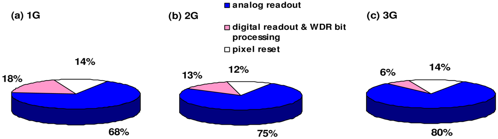
Generally, the power consumed by the three sensors is distributed among three main parts: (a) pixel operation during reset, when the photodiode is precharged; (b) analog readout, during which the pixel mantissa is read out of the pixel; and (c) the digital readout and WDR bits generation, during which the digital information of the DR extension is processed. The distribution between the different power sources is shown in
Figure 5.
The power that is dissipated during digital readout and WDR bit processing solely depends on the supply voltage (
VDD), capacitances, frame rate, and activity factors. However, the power dissipated by the analog readout and pixel reset also depends on the voltage swing of the imager, as shown in
Equation (9):
where
FR is the system's frame rate;
CS/H represents the sample and hold capacitance to which the pixel mantissa is readout; and
Vreset represents the reset level to which the pixel photodiode is initially precharged. Although
Equation (9) neglects some components, such as the power dissipated by analog biases, it clearly shows that assuming that all sensors present the same photodiode and sample and hold capacitances, the sensor with the maximum output swing will dissipate the most power. According to
Equations (6)–
(8), the power dissipated by the 3G sensor is the highest among the three discussed sensors, whereas the power of the 1G sensor is lowest, as can also be seen in
Table 5.
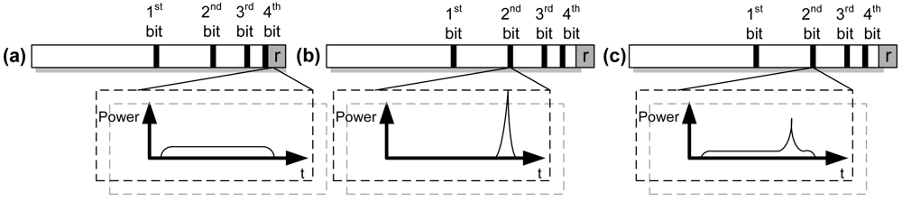
It is very interesting to examine the peak power profile of the imagers. The 1G imager operates in a rolling shutter mode; thus only a single row of the pixels is accessed each time. On the other hand, the 2G and 3G sensors operate in a global shutter mode; thus some operations, such as reset, are simultaneously applied to all the pixels within the array. Therefore, the peak power consumption occurs at different time points in the three presented sensors (
Figure 6a–c). In the 1G sensor, the peak power is consumed during the readout operation “
r” at the end of the frame. During this phase, the column-wise sample and hold capacitances, which are much larger than the photodiode capacitances, are charged by the SFs of the selected pixel row (
Figure 6a). On the other hand, in the 2G and 3G sensors, the peak power is reached during the global reset operation (
Figure 6b,c). This can occur during global reset at the beginning of the frame or after one of the four WDR bits are generated. For example, assuming that all the pixels within the array are reset after the 2nd bit is produced, the conditional reset is applied globally to the entire pixel array and peak power is reached.
The difference in power profiles between the 2G and 3G sensors is caused by the different WDR bit generation procedures. In the 2G sensor, the WDR bit is entirely generated inside the pixel. During this procedure the comparator decision is followed shortly by the conditional global reset operation. Therefore, the peak of power is relatively narrow and high, since it includes both the portion of photodiode precharge and the comparator decision. In the 3G sensor, WDR bit generation is partially performed outside the pixel, since the saturation detection is performed by the column-wide comparators that are located above the pixel array. During the saturation detection phase, each pixel row is sequentially checked and fed with the comparator decision. Only after all the rows have been processed, the conditional reset is globally applied to the pixel array. Thus, the peak caused by the reset is preceded with a certain rise in the power that is consumed by the comparators outside the pixel. Since the reset operation is separated in time from the comparator decision, the peak power is lower than that reached by the 3G sensor.
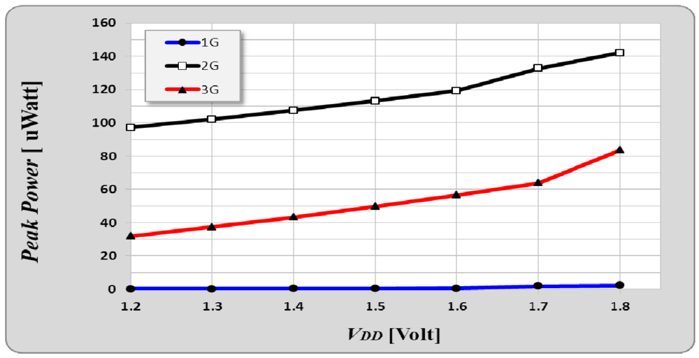
Figure 7 shows the peak power of all three sensors at different supply voltages. The peak power of both global shutter sensors exceeds the peak power generated by the 1G imager by almost three orders of magnitude, due to the global activation of the reset operation. However, it can be easily seen that the 2G imager has the greatest instant power consumption with accordance to the analysis of temporal power consumption given above.
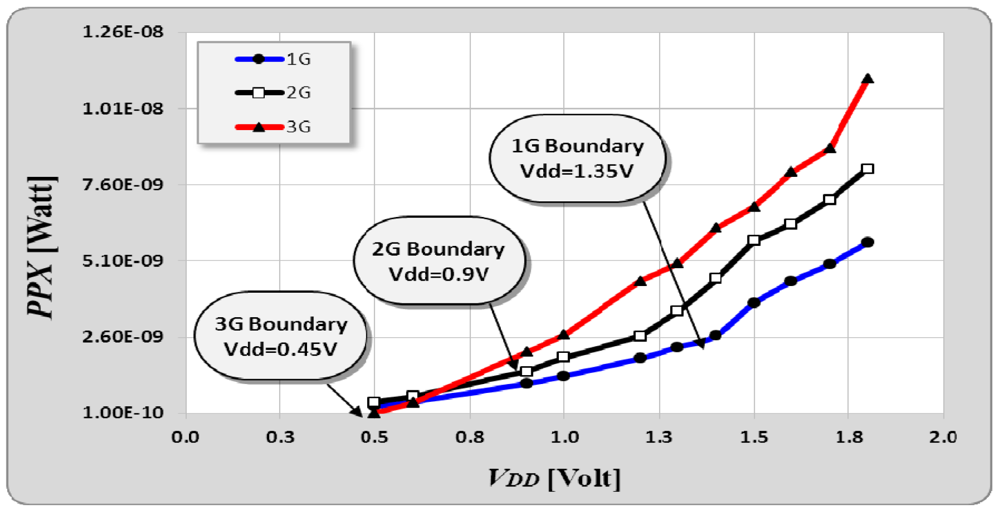
Figure 8 depicts the dependence of average Power Per Pixel (PPX)
versus VDD at the TT corner at room temperature. As expected, the power grows non-linearly with the supply voltage for all of the discussed sensors. Note that according to
(6)–
(8), each generation of sensor has a different “
Boundary VDD”, at which the mantissa cannot be retrieved from the pixel.
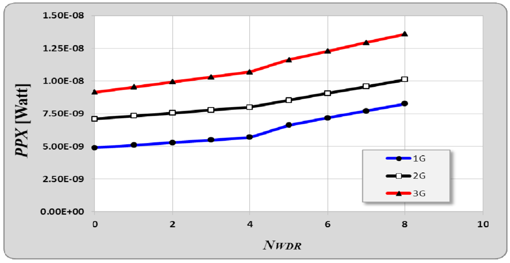
Another parameter that was examined is the influence of the WDR extension on the power dissipation of the imagers. The number of conditional resets is set by the number of WDR bits,
NWDR. As
NWDR increases, the number of reset operations increases and the power dissipation is expected to rise for each of the three discussed sensors.
Figure 9 shows that the PPX increases linearly with every additional WDR bit. It can be learned, that employing the multiple reset algorithm for widening DR results in close to a 50% increase in power dissipation, as compared to the power dissipation when no DR extension is performed.
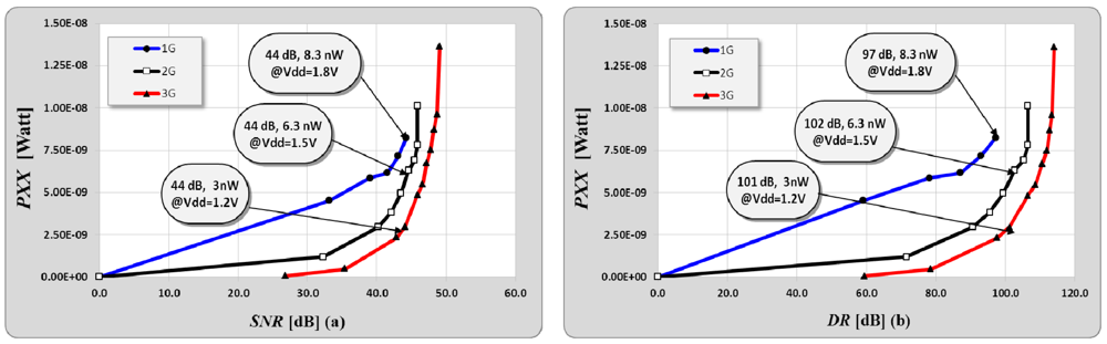
It was previously mentioned, that scaling down the supply voltage,
VDD, will significantly reduce the power consumption of the discussed sensors. However, doing so adversely affects the image quality in the sense of
Signal to Noise Ratio (SNR) and DR, as shown in
Figure 10. In order to present the maximum reachable SNR and DR, simulations with
NWDR = 8 were carried out.
Since the SNR and DR depend upon the maximum pixel level, the 3G sensor presents the highest SNR and DR. As the supply voltage scales down, the pixel level drops, and the SNR and DR decrease. If the reset level of the pixel photodiode (set by the supply voltage) is lower than the threshold voltage of the input transistor of the SF, it is impossible to retrieve the pixel mantissa. Therefore, the SNR and DR associated with that supply voltage drop to zero. Since the maximal pixel signal varies from one sensor to another
(6)–
(8), the boundary supply voltages, at which the sensors still can successfully operate, are different. For example, the boundary supply voltage for the 1G sensor is the highest one and is reached, when the
VDD is reduced from 1.8 V to 1.35 V. On the other hand, the boundary supply voltages for the 2G and 3G sensors are much lower due to their higher maximal pixel level, as compared to the 1G sensor. The 2G sensor ceases to operate at 0.9 V, whereas the operation boundary for the 3G sensor is 0.45 V. Thus, the last sensor is able to function at supply voltages as low as the threshold voltage of the transistor.
In order to address the tradeoffs between the supply voltage and the SNR/DR, we have calculated the power consumption per pixel
versus the SNR and DR (
Figure 11). This figure allows setting the optimal supply voltage,
VDD, according to the SNR and DR requirements of the designed sensor. For example, if the sensor SNR should be no less than 43 dB and DR should be no less than 95 dB, then according to
Figure 11, the appropriate supply voltages for the 1G, 2G and 3G sensors are 1.8 V, 1.5 V and 1.2 V, respectively. Note that according to the chosen SNR and DR requirements, the most effective sensor is the 3G sensor, in spite of the fact that it is more sensitive to
VDD changes and its maximal power dissipation exceeds that of the 1G and 2G sensors by 30%.


