Preparation and Spectrum Characterization of a High Quality Linear Variable Filter

1
Changchun Institute of Optics, Fine Mechanics and Physics, Chinese Academy of Sciences, Changchun 130033, China
2
College of Da Heng, University of Chinese Academy of Sciences, Beijing 100049, China
3
School of Optoelectronic Engineering, Changchun University of Science and Technology, Changchun 130000, China
*
Author to whom correspondence should be addressed.
Coatings 2018, 8(9), 308; https://doi.org/10.3390/coatings8090308
Submission received: 4 July 2018
/
Revised: 21 August 2018
/
Accepted: 24 August 2018
/
Published: 31 August 2018
(This article belongs to the Special Issue Applications of Optical Thin Film Coatings)
Abstract
:To meet the requirements for lightweight, miniaturized dispersive optical systems for space applications, linear variable filters with a high transmittance and spatial dispersion coefficient are proposed. The filters were produced with dual ion beam sputtering, where a single layer thickness variation was achieved with a deposition rate adjustment based on a linear variable correction formula. A linear variable trend matching method was used to correct the film thickness based on the reduction of the mismatch error between two materials: Ta2O5 and SiO2. The influence of the spectral and spatial measuring average effects was addressed by sampling the spot size optimization. This paper presents an all-dielectric linear variable filter that operates between 520 and 1000 nm, with an excellent linear dependence of 40 nm/mm over 12 mm. The linear variable filter possessed a 2.5% bandwidth, and its transmittance was found to be >80% at the central wavelength of the band, with a 0.1% transmittance in the cut-off region. These results indicate great potential for optical devices for space applications, and the developed process has good reproducibility and stability.
1. Introduction
As aerospace technology rapidly develops, increasing attention has been paid to optical experimental and detection equipment for space applications. Limited by environmental conditions and cost, optical systems in space applications are required to be lightweight and integrated [1,2]. Some traditional optical devices can no longer meet these requirements. Linear variable filters (LVFs), as a new type of dispersion device, have various advantages. Compared with traditional dispersion devices, such as prisms and gratings, they have a compact structure, and their bandpass transmission and bandwidth can be adjusted to the required operational wavelength [3,4]. Compared with multi-channel bandpass filters, they can act on a wider waveband, and their manufacturing process is relatively simple [5]. LVF provides a methodology for the design of miniaturized and integrated optical systems, particularly in the field of space technology [6].
The dispersion device described here is part of a spectrometer for space applications. The required operating spectrum is 520–1000 nm, the central wavelength gradient along the variable direction is required to be 40 nm/mm, the minimum peak transmittance is higher than 80%, the spectral out of band transmittance is less than 0.1%, and the transmission bandwidth is 2.5% of the central wavelength. In addition, the dispersion device should also be miniaturized and lightweight, and have a simple preparation and good repeatability. LVF refers to a narrow band filter corresponding to the linear variation passband spectrum at each spatial position in the gradient direction of the filter [7,8]. LVF has a high integration level (low weight, simple structure, and miniaturized), and its spectral coefficient can be adjusted according to the design requirements [9,10]. The efficiency of LVF beam splitting is higher than that of traditional dispersion devices, which is of great significance for the miniaturization and integration of optical systems in space applications [11,12].
There are two main types of LVF on the market: one type of LVF involves a mechanical combination of a long-wave-pass filter and short-wave-pass filter. This system is complex because more mechanical structures are needed, and it is difficult to achieve a bandwidth as narrow as 2.5% of the central wavelength. The other type of LVF is an independent narrow bandpass filter. Angela Piegari’s research team have developed an LVF using this design method. In the paper by Piegari et al. [6], the size of the prepared LVF is 2.1 mm, and the passband transmittance is about 60%. In our research, considering the requirements of dispersive optical systems in space and the size of the sensor, the size of the required LVF is 12 mm, the operating spectrum is between 520 and 1000 nm, and the transmittance should be >80% at the central wavelength of the band. This paper introduces the development process of an LVF with a high transmittance and high dispersion coefficient. A new linear variable correction formula is developed that can determine the linear variation of a single layer thickness more easily than in previous reports. The mismatch error of two materials is reduced using a linear variable trend matching method, which has not been reported before.
2. Experimental Details
2.1. Coating Design for LVF
The linear dispersion coefficient is the index that can measure the integration level of LVF. The linear dispersion coefficient is defined by the equation
where dstart and dend are the starting spatial position and ending spatial position of the LVF, respectively. For the bandpass filters, λstart and λend are the starting operating wavelength and the ending operating wavelength of the LVF, respectively, meaning the central wavelength of the bandpass filter at the starting spatial position and the ending spatial position.
As for applications, the linear dispersion coefficient of the LVF is in direct proportion to the density of the operating wavelength compression and the miniaturization degree. However, from the perspective of development, a large dispersion coefficient means a large change rate of deposition velocity and a great difficulty for development [13]. In this paper, on the premise of guaranteeing the accuracy and repeatability of the filter preparation, the linear dispersion coefficient of the variable filter was designed as 40 nm/mm so that a linear variable region, with the center wavelength from 520 to 1000 nm, can be obtained in the substrate range of 12 mm. As for the design of the films, in particular the discrete optical filter, the LVF is designed according to the interference principle of optical waves in multilayer optical film [14].
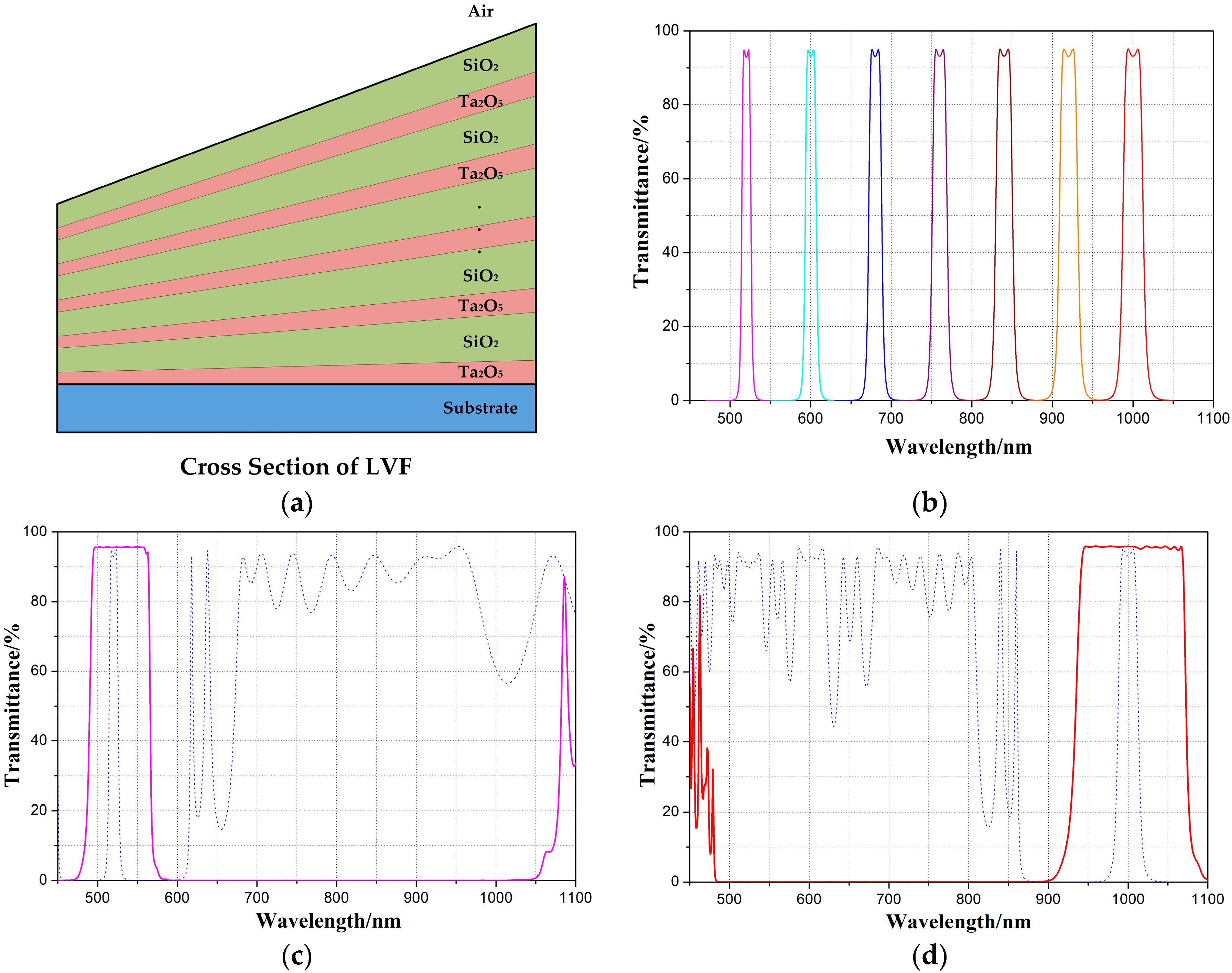
To meet the application requirements of an LVF, the substrate needs to be coated on both sides. On one side is a narrow band pass filter coating. The film is designed using the three cavities Fabry–Perot model, and the film structure is Sub|(HL)2 H 4L H (LH)2 L (HL)2 H 4L H (LH)2 L (HL)2 H 4L H (LH)2 L|. Air, Ta2O5, and SiO2 are used as high index materials (H) and low index materials (L) [15,16,17]. On the other side is a wide cut-off filter coating. The film is composed of long-wave-pass and short-wave-pass coatings. The wide cut-off filter coating has 182 layers, Ta2O5 and SiO2 are used as film materials, and the thickness was optimized to reach the design target. The narrow band pass filter coating and wide cut-off filter coating have the same linear variable rate. Therefore, in the process of coating on the other side, it is only necessary to ensure that one position of the narrow band-pass filter is matched with that of the wide cut-off filter, so that they can be aligned. The design of the wide cut-off film also has a margin for the cut-off region, which can eliminate the influence of the position error. In the process of film preparation, the film thickness in each cavity is controlled in real-time by a direct optical monitoring method, and the average time monitoring method is adopted to control the coupling layer thickness, which is used to connect each cavity. Due to the stability of the deposition rate of Veeco’s SPECTOR dual ion beam sputtering system, the film thickness of the wide cut-off filter is controlled by the time monitoring method. As shown in Figure 1a, the cross section of LVF is a wedge structure, the thickness of each layer varies linearly in one direction of the substrate, and the design spectrum of LVF at different wavelengths is shown in Figure 1b. The transmission bandwidth is 2.5% of the central wavelength, as shown in Figure 1c,d, and the cut-off region is extended to 520–1000 nm by the coating on both sides.
2.2. Preparation and Film Thickness Matching of LVF
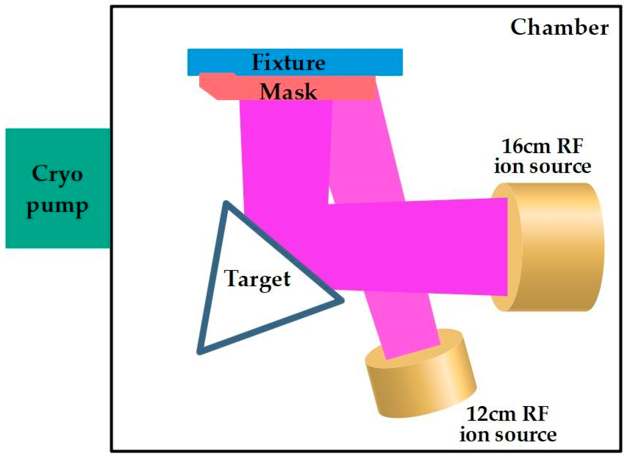
In this paper, LVF was prepared by dual ion beam sputtering technology (Veeco, Plainview, NY, USA) [18,19]. Because of the high energy of the deposited particles in the process of preparation, the films prepared by dual ion beam sputtering have good optical stability, environmental stability, and repeatability. The Veeco’s SPECTOR dual ion beam sputtering optical coating system is shown in Figure 2.
The film thickness correction masks were placed in front of the sample fixture. The deposition rate of the film material is determined by the sputtering power of the 16 cm RF ion source and the shielding ratio of the mask. The sputtering distribution of the film material depends on the incident angle of the ion beam relative to the target and the sputtering characteristics of the film material [20]. In the process of thin film deposition, O2 should be supplied to the 12 cm auxiliary ion source to ensure the oxidation degree of the film materials.
The optical thickness of each layer should change linearly along the length in order to realize the linear variation of the central wavelength of the passband of the LVF along the substrate length [21]. Therefore, the linear dispersion coefficient of the LVF can be accurately controlled by accurately controlling the thickness of each layer and its changing rate in relation to the substrate position. The linear variation of the film thickness was achieved by installing a suitable thickness correction mask in front of the substrate [22,23]. Based on the principle that the thickness of the film prepared at various points on the surface of the substrate is proportional to the angle exposed to the film material beam during sputtering deposition under a uniform rotation of the fixture, this paper established the linear variable correction formula (Equation (2)), combined it with the density distribution of the sputtering film material in the vacuum chamber of the coating machine and designed the shape of the masks.
As shown in Figure 3, the dark area is the designed correction mask, which was fixed in front of the substrate fixture, and the angle indicated in Figure 3 is the shielding angle (θt in Equation (2) and Table 1) of each sample on the substrate. During the sputtering deposition process, the substrate fixture rotates at a constant speed, and the time during which different positions on the substrate are exposed to the film material beam is different, so the thickness of each layer changes linearly.
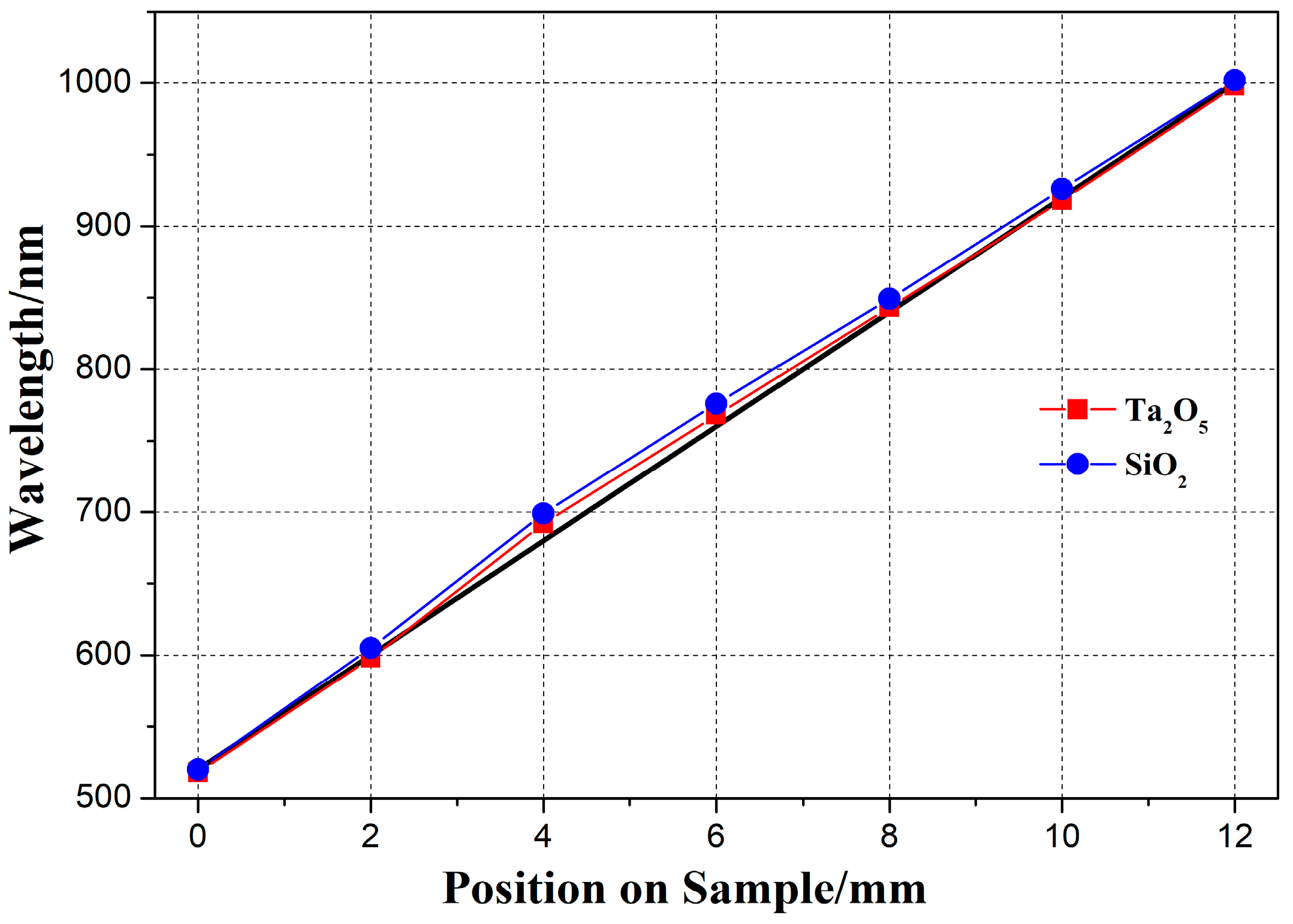
According to the above method, the masks for Ta2O5 and SiO2 were linearly corrected. The linear change rate of the thickness of the two materials after correction is shown in Figure 4.
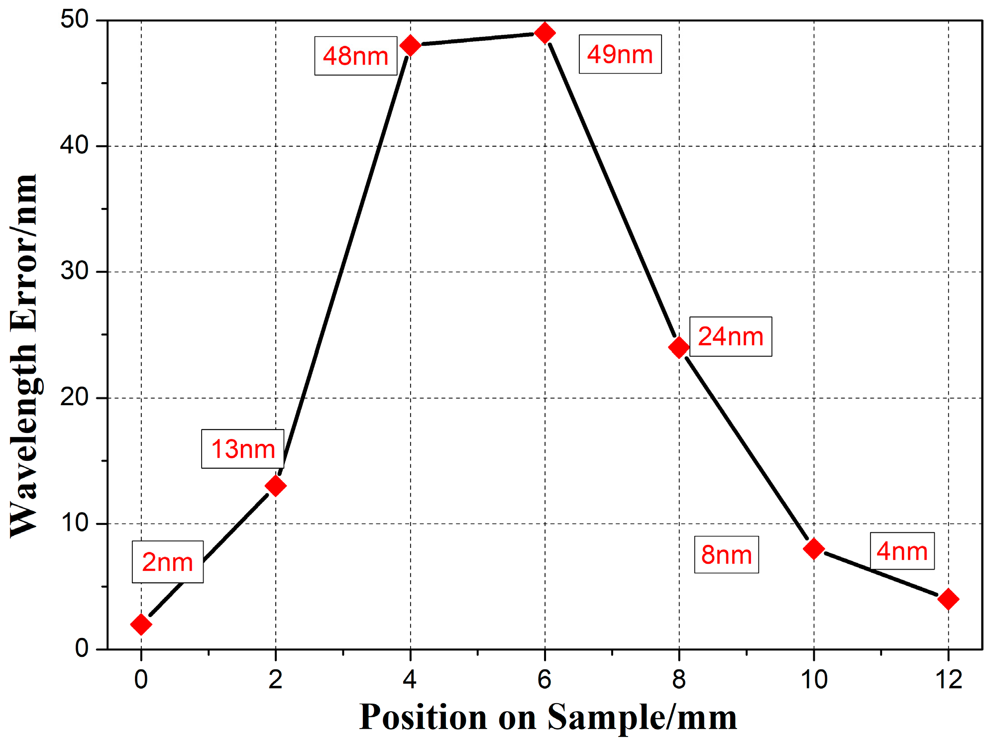
As shown in Figure 4, the two materials can basically meet the linear variable rate of 40 nm/mm, required in the design. However, due to the difference in sputtering between the characteristics of the two materials, the distribution of the sputtered films is different in the same sputtering environment. In some sampling points, the two materials are seriously mismatched, and the mismatching error of the film thickness is shown in Figure 5.
The mismatching error of the film thickness not only results in the deviation of the central wavelength, but also seriously affects the peak transmittance of the bandpass filter. Therefore, the mismatch of materials is an important reason for low transmittance. In order to reduce the mismatch error between the two materials, Ta2O5 and SiO2, the trend matching method was used to optimize the original corrected mask. To be specific, the deposition thickness of one film material was fixed at the sampling point with a serious mismatch, and the other film material was corrected according to the mismatch ratio in the error direction. Ta2O5 has good sputtering stability and accurately calibrates the film thickness. Therefore, the constant change rate of SiO2 was selected to carry out a trend match of the change rate of Ta2O5. The linear change rates of the thickness of the two materials after match correction are shown in Figure 6. The mismatch error of the two film materials was significantly reduced. The deposition rates of Ta2O5 and SiO2 in each sample are shown in Table 2.
3. Results and Discussion
The LVF, prepared according to the optimized process parameters, is shown in Figure 7. The spectrum of LVF changes in relation to the substrate position, and its central wavelength continuously varies in relation to the linear dispersion coefficient in the operating direction of the filter. The linear dispersion coefficient of the designed film system is 40 nm/mm, which means that the measured spectrum within a certain sampling range is the average value within the region. The average spectral and spatial effect can deform the measured spectral curve and decrease the transmittance of the central wavelength [24]. The specific transmittance is shown in Equation (3):
where T(x,λ) is the transmittance, with the wavelength of λ, when the center of the sampling region is located at x on the substrate, 2d is the length of the sampling spot, and the region on the substrate for calculating the average spectrum within a sampling range is from (x − d) to (x + d). The results of the analysis of the linear variable bandpass filter, designed according to the size of the test spot through Equation (3), are shown in Figure 8. As shown in Figure 8, the cut-off steepness of the test spectral curve becomes worse, and the transmittance of the central wavelength decreases as the size of the test spot increases.
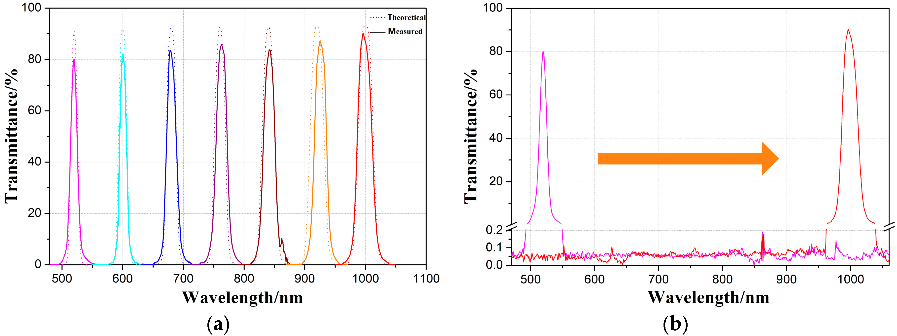
In order to overcome the influence of the average spectral and spatial effects on the measurement results and obtain more accurate measurement results, the micro-spot test method was used to optimize the sampling spot of the measurement system. The measurement principle is shown in Figure 9a. The small spot was obtained through the precise slit diaphragm. The lens converged the test beam to enhance the optical density of the sample surface, reducing the error caused by the test noise. According to the above principle, the test accessory shown in Figure 9b was developed for a Perkin-Elmer’s Lambda1050 spectrophotometer (Waltham, MA, USA). In the measurement process, the sampling points were taken at intervals of 2 mm along the change direction of wavelength, and the diameter of the sampling spot was 0.2 mm. The measured transmittance spectrum of each sampling point is shown in Figure 10.
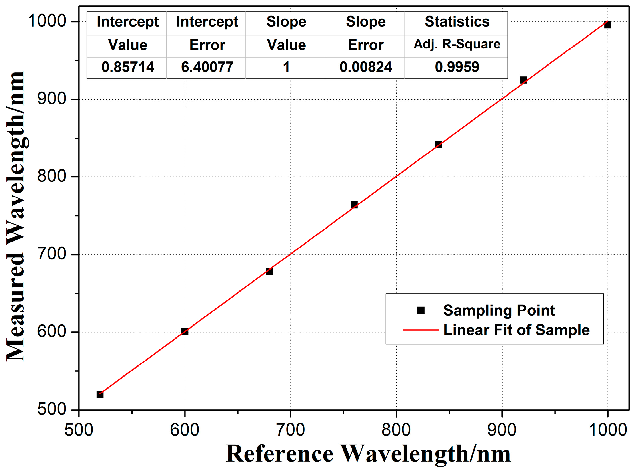
As shown in Figure 10a, the measured spectrum is basically consistent with the theoretical spectrum of Spot = 0.2 mm. The peak transmittance of the central wavelength at each sampling point is more than 80%, and the full width at half maximum (FWHM) changes linearly from 12.8 to 24.7 nm in the operating range, which is almost consistent with 2.5% of the central wavelength. As shown in Figure 10b, the cut-off region transmittance is less than 0.1% in the operating spectrum of 520 to 1000 nm. The measured spectral parameters of the experimental samples fit well with the designed parameters. After repeated preparation under the same conditions, the transmittance characteristics were basically the same under the same process conditions. The process has good repeatability, and the dual ion beam sputtering system has great advantages in stability. In order to verify the linear dispersion coefficient of the experimental samples, the central wavelength position of each sampling point was calculated by linear fitting, and the curve is shown in Figure 11.
As shown in Figure 11, the Adj. R-Square is 0.9959, which indicates that the linear correlation between the measured wavelength and the reference wavelength is almost uniform. The central wavelength gradient is basically consistent with 40 nm/mm. According to the above test, the optical characteristics of the prepared LVF can reach the theoretical design target and meet the usage requirements of the integrated optical system.
4. Conclusions
In this paper, the deposition technique of dual ion beam sputtering was used to prepare an LVF with a high transmittance and high dispersion coefficient by adjusting the deposition rates of the thin film materials through the establishment of a linear variable correction formula. In the thickness correction process of the different film materials, the mismatch error of the two film materials was reduced through the linear variable trend matching method. The average spectral and spatial effect was overcome, and the accurate spectral data of LVF at different positions were obtained using the micro-spot test method. The prepared LVF operates between 520 nm and 1000 nm, which is achieved with an excellent linear dependence of 40 nm/mm over 12 mm. The linear variable filter possessed a 2.5% bandwidth, transmittance was found to be >80% at the central wavelength of the band, with a 0.1% transmittance in the cut-off region. The test results show that the prepared LVF has good spectral characteristics and meets the requirements of integrated and miniaturized optical systems for space applications.
Author Contributions
Conceptualization, J.G. and H.T.; Methodology, J.G. and H.T.; Validation, H.T. and J.Z.; Formal Analysis, H.T. and J.Z.; Investigation, J.Z. and X.W.; Data Curation, H.T., X.W., and X.F.; Writing—Original Draft Preparation, H.T.; Writing—Review & Editing, H.T., J.Z., and X.F.
Funding
This research was funded by the National Natural Science Foundation of China (61705224).
Acknowledgments
Thanks to Key Laboratory of Optical System Advanced Manufacturing Technology Chinese Academy of Sciences for supporting the experiment.
Conflicts of Interest
The authors declare no conflict of interest.
References
- Emadi, A.; Wu, H.; de Graaf, G.; Wolffenbuttel, R. Design and implementation of a sub-nm resolution microspectrometer based on a linear-variable optical filter. Opt. Express 2012, 20, 489–507. [Google Scholar] [CrossRef] [PubMed]
- McLeod, R.R.; Honda, T. Improving the spectral resolution of wedged etalons and linear variable filters with incidence angle. Opt. Lett. 2005, 30, 2647–2649. [Google Scholar] [CrossRef] [PubMed]
- Sheng, B.; Chen, P.; Tao, C.; Hong, R.; Huang, Y.; Zhang, D. Linear variable filters fabricated by ion beam etching with triangle-shaped mask and normal film coating technique. Chin. Opt. Lett. 2015, 13, 122301. [Google Scholar] [CrossRef]
- Williams, C.; Rughoobur, G.; Flewitt, A.J.; Wilkinson, T.D. Single-step fabrication of thin-film linear variable bandpass filters based on metal–insulator–metal geometry. Appl. Opt. 2016, 55, 9237–9241. [Google Scholar] [CrossRef] [PubMed]
- Ji, P.; Gao, S.; Park, C.-S.; Lee, S.-S.; Choi, D.-Y. Linear variable filter enabling an enhanced wavelength gradient based on shadow-mask sputtering. Microw. Opt. Technol. Lett. 2017, 59, 3142–3146. [Google Scholar] [CrossRef]
- Piegari, A.; Bulir, J.; Sytchkova, A.K. Variable narrow-band transmission filters for spectrometry from space. 2. fabrication process. Appl. Opt. 2008, 47, C151–C156. [Google Scholar] [CrossRef] [PubMed]
- Mokhtari, A.; Jamshidi, K.; Preußler, S.; Zadok, A.; Schneider, T. Tunable microwave-photonic filter using frequency-to-time mapping-based delay lines. Opt. Express 2013, 21, 21702–21707. [Google Scholar] [CrossRef] [PubMed]
- Diest, K.; Dionne, J.A.; Spain, M.; Atwater, H.A. Tunable color filters based on metal−insulator−metal resonators. Nano Lett. 2009, 9, 2579–2583. [Google Scholar] [CrossRef] [PubMed]
- Wiesent, B.R.; Dorigo, D.G.; Koch, A.W. Limits of IR-spectrometers based on linear variable filters and detector arrays. In Instrumentation, Metrology, and Standards for Nanomanufacturing IV, Proceedings of Instrumentation, Metrology, and Standards for Nanomanufacturing IV, San Diego, CA, USA, 2–4 August 2010; Postek, M.T., Ed.; SPIE: Bellingham, WA, USA, 2010; Volume 7767. [Google Scholar] [CrossRef]
- Murr, P.J.; Schardt, M.; Koch, A.W. Static hyperspectral fluorescence imaging of viscous materials based on a linear variable filter spectrometer. Sensors 2013, 13, 12687–12697. [Google Scholar] [CrossRef] [PubMed]
- Law, C.S.; Santos, A. Realisation and optical engineering of linear variable bandpass filters in nanoporous anodic alumina photonic crystals. Nanoscale 2017, 9, 7541–7550. [Google Scholar] [CrossRef]
- Hendrix, K. Linear variable filters for NASA’s OVIRS instrument: Pushing the envelope of blocking. Appl. Opt. 2017, 56, C201–C205. [Google Scholar] [CrossRef] [PubMed]
- Ghaderi, M.; Ayerden, N.P.; Emadi, A.; Enoksson, P.; Correia, J.H.; de Graaf, G.; Wolffenbuttel, R.F. Design, fabrication and characterization of infrared LVOFs for measuring gas composition. J. Micromech. Microeng. 2014, 24, 084001. [Google Scholar] [CrossRef]
- Willey, R.R. Achieving narrow bandpass filters which meet the requirements for DWDM. Thin Solid Films 2001, 398–399, 1–9. [Google Scholar] [CrossRef]
- Tien, C.L. Influence of ejection angle on residual stress and optical properties of sputtering Ta2O5 thin films. Appl. Surf. Sci. 2008, 255, 2890–2895. [Google Scholar] [CrossRef]
- Tabata, A.; Matsuno, N.; Suzuoki, Y.; Mizutani, T. Optical properties and structure of SiO2 films prepared by ion-beam sputtering. Thin Solid Films 1996, 289, 84–89. [Google Scholar] [CrossRef]
- Shang, P.; Xiong, S.; Li, L.; Tian, D.; Ai, W. Investigation on thermal stability of Ta2O5, TiO2 and Al2O3 coatings for application at high temperature. Appl. Surf. Sci. 2013, 285, 713–720. [Google Scholar] [CrossRef]
- Nguyen, J.; Yu, J.S.; Evans, A.; Slivken, S.; Razeghi, M. Optical coatings by ion-beam sputtering deposition for long-wave infrared quantum cascade lasers. Appl. Phys. Lett. 2006, 89, 111113. [Google Scholar] [CrossRef]
- Malobabic, S.; Jupé, M.; Ristau, D. Spatial separation effects in a guiding procedure in a modified ion-beam-sputtering process. Light Sci. Appl. 2016, 5, e16044. [Google Scholar] [CrossRef]
- Çetinörgü, E.; Baloukas, B.; Zabeida, O.; Klemberg-Sapieha, J.; Martinu, L. Optical and tribomechanical stability of optically variable interference security devices prepared by dual ion beam sputtering. Appl. Opt. 2011, 50, 3351–3359. [Google Scholar] [CrossRef] [PubMed]
- Ko, C.-H.; Chang, K.-Y.; Huang, Y.-M. Analytical modeling and tolerance analysis of a linear variable filter for spectral order sorting. Opt. Express 2015, 23, 5102–5116. [Google Scholar] [CrossRef] [PubMed]
- Abel-Tibérini, L.; Lemarquis, F.; Lequime, M. Masking mechanisms applied to thin-film coatings for the manufacturing of linear variable filters for two-dimensional array detectors. Appl. Opt. 2008, 47, 5706–5714. [Google Scholar] [CrossRef] [PubMed]
- Hsu, J.-C. Analysis of the thickness uniformity improved by using wire masks for coating optical bandpass filters. Appl. Opt. 2014, 53, 1474–1480. [Google Scholar] [CrossRef] [PubMed]
- Murr, P.J.; Wiesent, B.R.; Hirth, F.; Koch, A.W. Thin film measurement system for moving objects based on a laterally distributed linear variable filter spectrometer. Rev. Sci. Instrum. 2012, 83, 035110. [Google Scholar] [CrossRef] [PubMed]
Figure 1.
(a) The wedge structure of LVF; (b) the design pass band spectrum of LVF at different wavelengths; both sides of the design spectrum of LVF at the (c) beginning (520 nm) and (d) end (1000 nm).
Figure 1.
(a) The wedge structure of LVF; (b) the design pass band spectrum of LVF at different wavelengths; both sides of the design spectrum of LVF at the (c) beginning (520 nm) and (d) end (1000 nm).

Figure 2.
Dual ion beam sputtering system.

Figure 3.
Schematic diagram of correction mask.
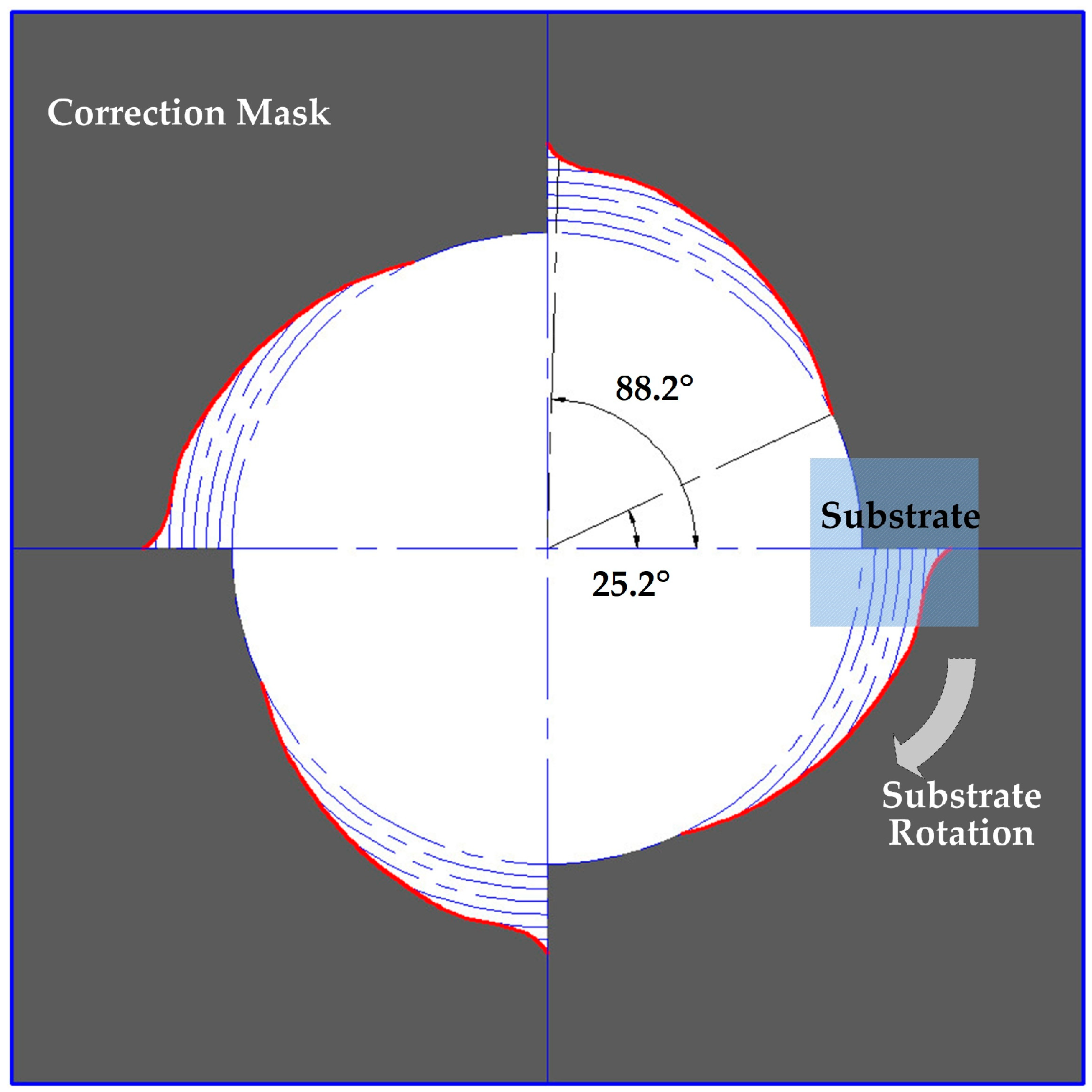
Figure 4.
Linear change rate of the thickness of the two materials.
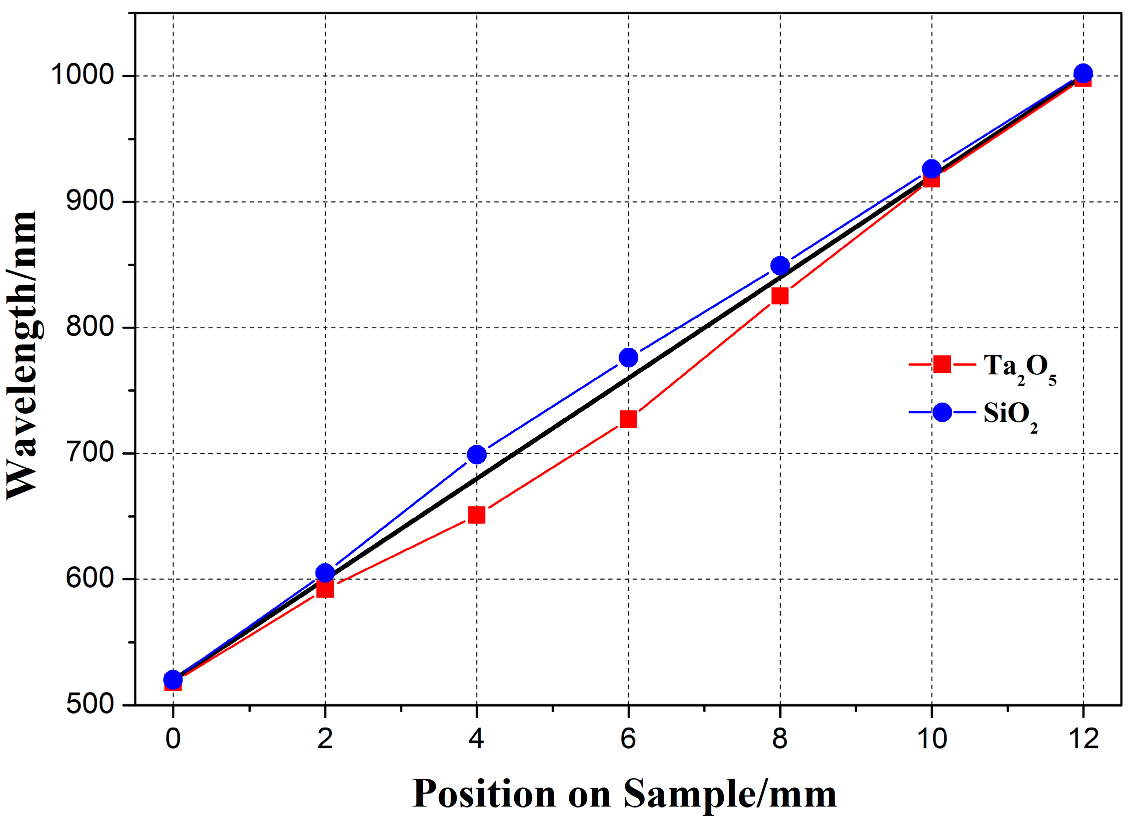
Figure 5.
Film thickness mismatching error in sampling points.

Figure 6.
Linear change rate of the thickness of the two materials after match correction.

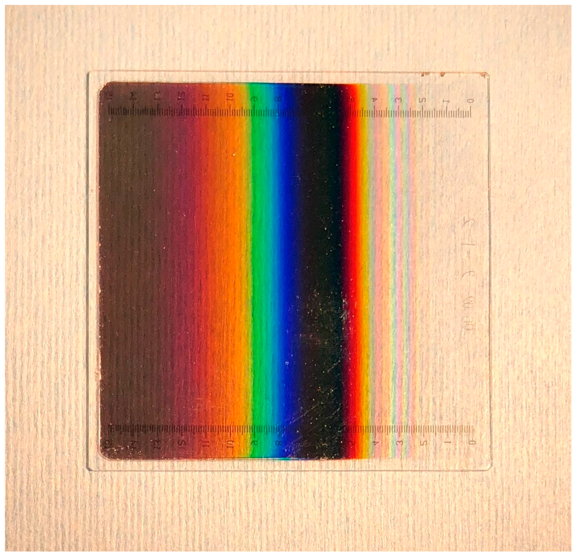
Figure 7.
Sample photograph of the developed LVF.

Figure 8.
Transmission spectral curves with different sizes of the test spot.
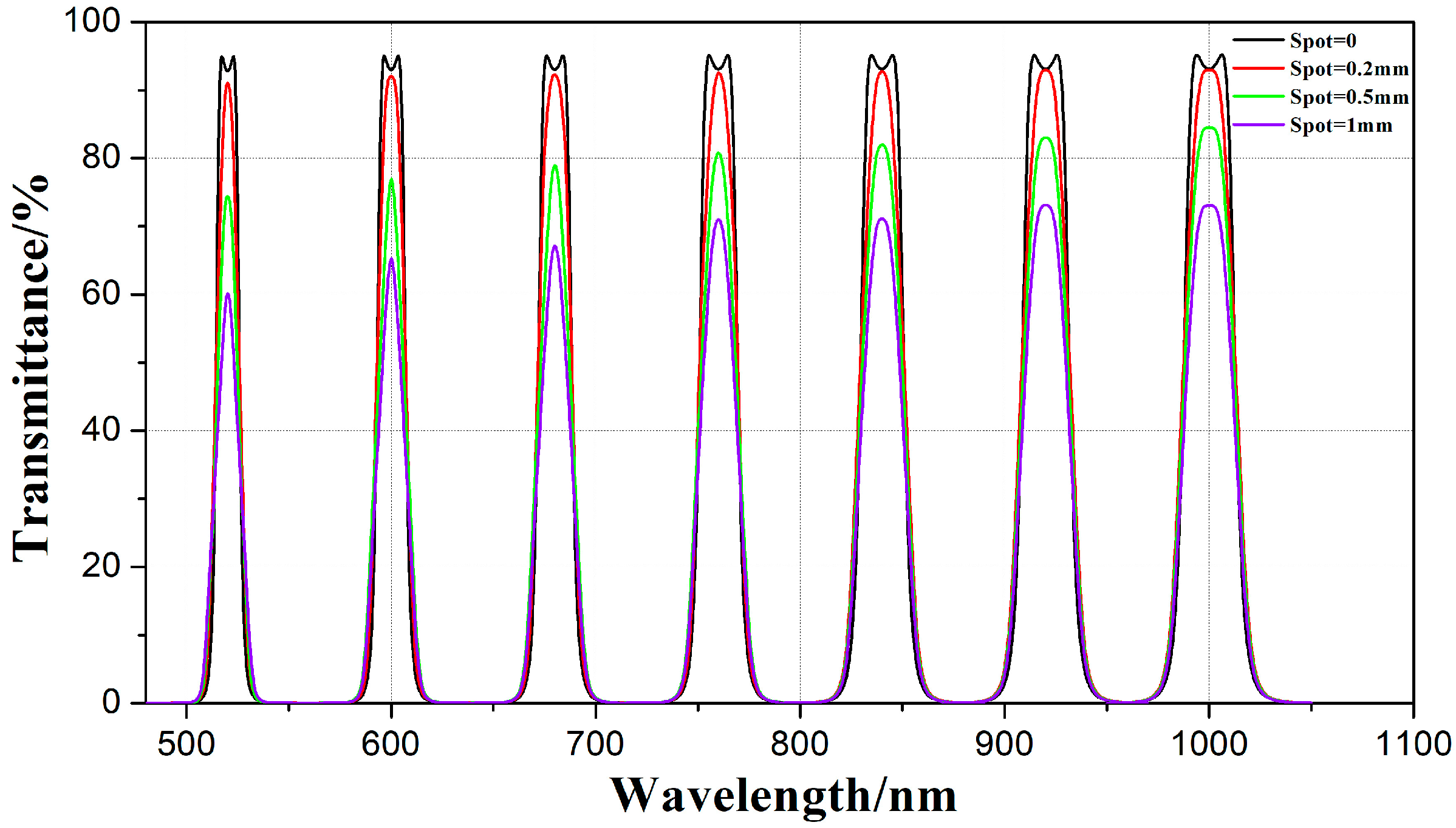
Figure 9.
The micro-spot test method. (a) The measurement principle and (b) the developed test accessory for a Lambda1050 spectrophotometer.
Figure 9.
The micro-spot test method. (a) The measurement principle and (b) the developed test accessory for a Lambda1050 spectrophotometer.
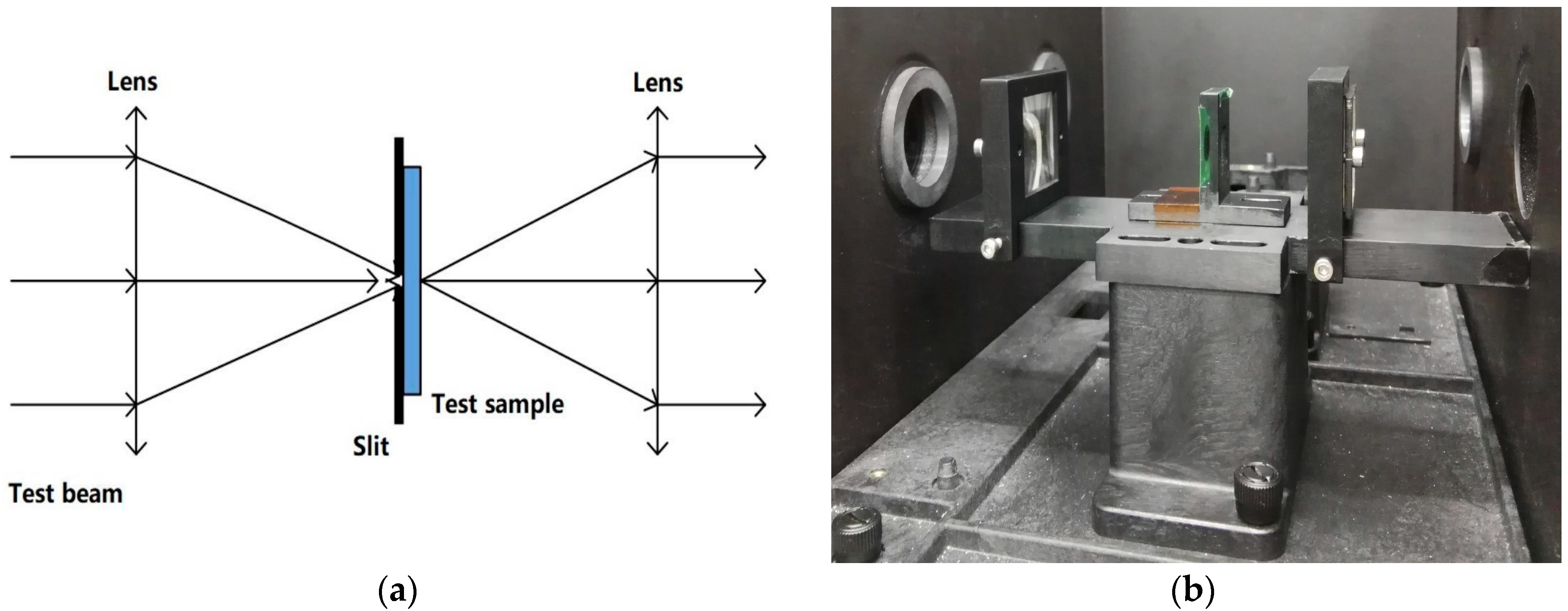
Figure 10.
Measured spectrum of LVF when Spot = 0.2 mm. (a) Measured and theoretical transmittance spectrum for each sampling point and (b) measured transmittance spectrum in the whole operating range of 520–1000 nm.
Figure 10.
Measured spectrum of LVF when Spot = 0.2 mm. (a) Measured and theoretical transmittance spectrum for each sampling point and (b) measured transmittance spectrum in the whole operating range of 520–1000 nm.

Figure 11.
Linear fitting curve of the central wavelength.

Table 1.
Revised data of LVF with the mask.
| Position on Sample/mm | d0 (nm) | d1 (nm) | dt (nm) | θ1 (°) | θt (°) |
|---|---|---|---|---|---|
| 0 | 1175 | 507 | 520 | 90 | 88.2485 |
| 2 | 1179 | 508 | 600 | 90 | 77.66021 |
| 4 | 1184 | 511 | 680 | 90 | 67.3997 |
| 6 | 1185 | 514 | 760 | 90 | 57.00447 |
| 8 | 1190 | 518 | 840 | 90 | 46.875 |
| 10 | 1182 | 519 | 920 | 90 | 35.56561 |
| 12 | 1186 | 522 | 1000 | 90 | 25.21084 |
Table 2.
Deposition rates of Ta2O5 and SiO2 in each sample on the substrate.
| Position on Sample (mm) | Deposition Rate of Ta2O5 (nm/s) | Deposition Rate of SiO2 (nm/s) |
|---|---|---|
| 0 | 0.1079 | 0.1017 |
| 2 | 0.1262 | 0.1186 |
| 4 | 0.1466 | 0.1372 |
| 6 | 0.1635 | 0.1524 |
| 8 | 0.1799 | 0.1671 |
| 10 | 0.1961 | 0.1824 |
| 12 | 0.2134 | 0.1975 |
© 2018 by the authors. Licensee MDPI, Basel, Switzerland. This article is an open access article distributed under the terms and conditions of the Creative Commons Attribution (CC BY) license (http://creativecommons.org/licenses/by/4.0/).
Share and Cite
MDPI and ACS Style
Tang, H.; Gao, J.; Zhang, J.; Wang, X.; Fu, X. Preparation and Spectrum Characterization of a High Quality Linear Variable Filter. Coatings 2018, 8, 308. https://doi.org/10.3390/coatings8090308
AMA Style
Tang H, Gao J, Zhang J, Wang X, Fu X. Preparation and Spectrum Characterization of a High Quality Linear Variable Filter. Coatings. 2018; 8(9):308. https://doi.org/10.3390/coatings8090308
Chicago/Turabian StyleTang, Haolong, Jinsong Gao, Jian Zhang, Xiaoyi Wang, and Xiuhua Fu. 2018. "Preparation and Spectrum Characterization of a High Quality Linear Variable Filter" Coatings 8, no. 9: 308. https://doi.org/10.3390/coatings8090308
Note that from the first issue of 2016, this journal uses article numbers instead of page numbers. See further details here.