Article

Growth of Magnetron-Sputtered Ultrathin Chromium Films: In Situ Monitoring and Ex Situ Film Properties

by
Alexandr Belosludtsev
1,*,
Anna Sytchkova
2,*,
Kazimieras Baltrusaitis
1,
Viktoras Vaicikauskas
1,
Vitalija Jasulaitiene
1 and
Tatjana Gric
1,3
1
Center for Physical Sciences and Technology, 02300 Vilnius, Lithuania
2
Optical Coatings Group, ENEA Casaccia, 00123 Roma, Italy
3
Department of Electronic Systems, VILNIUS TECH, 10223 Vilnius, Lithuania
*
Authors to whom correspondence should be addressed.
Coatings 2023, 13(2), 347; https://doi.org/10.3390/coatings13020347
Submission received: 17 January 2023 / Revised: 26 January 2023 / Accepted: 28 January 2023 / Published: 2 February 2023
(This article belongs to the Special Issue Advances in Optical and Optoelectronic: Materials and Applications)

Abstract

:
We report a systematic nanoscale investigation on the ultrathin Cr film growth process and properties. Polycrystalline metallic films were manufactured by magnetron sputtering on fused silica substrates. The film growth was observed in situ by broad-band optical monitoring (BBM) and plasma-emission spectroscopy (OES) methods. The ex situ characterization of the Cr films with thicknesses varying from 2.6 nm up to 57 nm were performed by both non-destructive and destructive techniques. Recently, we reported on a novel set of data for optical and electrical properties of sputtered chromium films. The optical and electrical properties of the films are known to be governed by their structure and microstructure, which were analyzed in detail in the present research. Moreover, the optical properties of the films were studied here in a significantly wider optical range and obtained using both in situ and ex situ measurements. Reliable in situ nanoscale characterization of metal films was shown to ensure an unfailing approach in obtaining ultrathin layers with desirable thickness and stable and well-determined optical constants and electrical conductivity. This is of high importance for various industries and novel upcoming applications.

1. Introduction

Chromium (Cr) is a widely used transition metal that finds application in engineering [1], optoelectronics [2,3], and plasmonics [4]. Chromium films can also be used as adhesive layers [5], as spacer layers [6], as dopants [7,8], for photomasking in lithography [9], as resistors [10], as an interlayer of magnetic multilayer coatings [11], as metallic coatings to increase the resistance to environmental degradation of less corrosion-resistant metals or alloys [12], for accident-tolerant nuclear fuel claddings [13], in metameric interference thin films [14], and as decoration [15]. Chromium films are used in the engineering of various optical components. For example, chromium can be used as a light-absorbing layer in solar absorbers [16,17], for emission enhancement [7], in display applications [18], in the automotive industry [19], and in tunable filters [20].
Ultrathin metal films are of keen interest because of their unique optical and electrical properties [2,3,4,14,19,21,22]. Metal films of nanometer-scale thicknesses are semi-transparent in a wide spectral range. Moreover, the optical properties of ultrathin metal films can be easily tuned by simply varying their thickness, hence allowing for the creation of coatings with sophisticated spectral performance. Furthermore, they have very good adhesion to various substrates. Finally, by a very small change of thickness, it is possible to significantly change the optical properties of the films; hence, the use of ultrathin metal layers opens more possibilities for manufacturing tunable optics.
A potential drawback in the utilization of ultrathin transparent conductive thin metal films is their fast degradation due to environmental agents such as moisture, air gases, and temperature variation. In contrast with most metals, for chromium, oxidation does not lead to the formation of a continuous oxide layer, and even at long exposures, a fraction of the chromium surface retains its metallic nature, even at the top layers [23].
Magnetron sputtering is a well-established deposition technique. It has a long history with successful development [24,25,26,27]. Among the benefits of the magnetron sputtering process, its stability should be underlined, as well as fast deposition rate, wide choice of materials suitable for deposition by this technique, high repeatability rate, good film uniformity, and excellent process control and simplicity of scaling up.
In our previous paper [28], we investigated the optical properties of ultrathin chromium films. Before our research, no systematic study of the magnetron-sputtered ultrathin chromium films’ optical, structural, and electrical properties was available in the literature. In that publication, we introduced our approach to optical property characterizations in detail. This research instead is dedicated to the in situ analysis and comparison to ex situ investigation of magnetron-sputtered ultrathin chromium films. The film composition and morphology are known to influence and explain its macroscopic properties, and therefore we here focused on the chemical and phase composition of the films and report on their surface morphology. Additionally, we provide the film optical properties in a much larger optical range. For the first time, the growth process was studied by in situ broad-band spectral monitoring enabling a nanoscale follow-up of the growing film transmittance. The ex situ characterization of the films for their optical, structural, microstructural, and electrical properties enabled an in-depth insight into the film formation and stabilization processes.

2. Experimental Details

Chromium films were sputtered using an unbalanced magnetron source with a planar target (Cr, 99.95% purity, diameter of 101.6 mm and thickness of 6 mm, Matsurf Technologies Inc., St. Paul, MN, USA) in a Kurt J. Lesker (Jefferson Hills, PA, USA) sputtering system (PVD225). The system was initially pumped down to a base pressure below 3 × 10⁻⁷ Torr. The magnetron was driven by a pulsed DC power supply. In this work, the repetition frequency was 100 kHz, the duty cycle was 80%, and the fixed power was 300 W. The argon (Ar, >99.999% pure) flow rate was 20 sccm, and the pumping speed was adjusted to attain the argon pressure at the same value of 2.2 mTorr. The settings of the Ar flow rate and the pumping speed were not changed during the experiments. Prior to every experiment, the target was pre-sputtered for 5 min to remove impurities and possible surface oxides. The system was equipped with a magnetron and substrate shutters. The experiments were conducted at room temperature and without substrate biasing. The target-to-substrate distance was 230 mm. Optimization of the substrate holder to target distance and of the sample placement for the best uniformity was performed. Measured values confirmed +/− 0.1% uniformity over the 25.4 mm area where the substrates were positioned for the coating depositions. For all the samples, an area positioned in the middle of the sample was selected for in-situ and ex-situ mesurements of the film properties.
The films were deposited on 1 mm thick fused silica (FS) substrates of 25.4 mm in diameter. The substrate was double-side polished at λ/10. The film growth was monitored by Insoptics Sp.z.O.O. (Poznan, Poland) optical broadband monitoring (BBM). The BBM transmittance spectra were recorded in the 400–1000 nm wavelength range. The highest film thickness was measured after deposition at the film edge by profilometry Dektak 150 (Veeco, Plainview, NY, USA) in order to estimate the deposition rate, which was 1.5 Å/s. The film thickness was controlled by the deposition time.
Direct transmittance and specular reflectance spectra of the manufactured films were measured ex situ in the 300–2500 nm wavelength range using a Photon RT (EssentOptics Europe, Vilnius, Lithuania) spectrophotometer operating at normal incidence in transmittance and (in reflection) at the angle of 8° in reflectance mode.
The elemental composition of films was investigated by X-ray photoelectron spectroscopy (XPS). The XPS characterization was carried out using a Kratos (Manchester, UK) AXIS Supra+ spectrometer with monochromatic Al Kα (1486.6 eV) X-ray radiation powered at 225 W. The base pressure in the analysis chamber was less than 1 × 10⁻⁹ mbar, and a low electron flood gun was used as a charge neutralizer. The survey spectra for each sample were recorded at pass energy 160 eV in 1 eV step and high-resolution spectra (pass energy 10 eV, in 0.1 eV steps) over individual element peaks. The binding energy scale was calibrated by setting the C1s hydrocarbon peak at 284.8 eV. For surface cleaning, the monoatomic Ar+ ions gun (Minibeam 6) was used.
For time-resolved optical emission spectroscopy (OES), a Nova Fabrica Ltd. (Ignalina, Lithuania) Inteleg® 2B-PEM (Broad-Band Plasma Emission Monitoring) system (Model Number: I2BPEM-341D015000) was used. The 2B-PEM detector covers a spectral range of 200–1100 nm with a 3 nm resolution. A fiber-optic optical monitoring assembly comprising a collection lens and a collimator tube inside the process chamber was placed. It collects the light originating from dense plasma 1 cm above the target surface, integrating the light along the width of the plasma.
The Infrared spectral measurements were performed in the range of 350–4000 cm−1 using a Thermo Electron Nicolet 8700 Fourier transform infrared (FTIR) spectrometer from Thermo Fisher Scientific (Waltham, MA, USA). It was equipped with a reflectance accessory and operated at an incidence angle of 10°.
To determine the optical constants of the films, ellipsometric measurements were performed using a J.A. Woolam (Lincoln, NE, USA) VW-VASE instrument in the spectral range 260–2500 nm at three incidence angles of 55°, 65°, and 75°.
Surface topography was measured using a Dimension Edge atomic force microscope, (AFM) from Bruker (Billerica, MA, USA) in tapping mode, over a 10 × 10 μm scan area. The AFM probe was an Al and diamond-like carbon (DLC)-coated Si probe of <15 nm tip radius.
X-ray diffraction (XRD), Fourier transform infrared (FTIR) spectroscopy, ellipsometry, and X-ray reflectometry (XRR) were used for the evaluation of film phase, thickness, density, and optical constants. These results and detailed optical and electrical properties evaluation are described in a dedicated paper [28].

3. Results and Discussion

3.1. Plasma Emission Monitoring and Elemental Composition

Firstly, the in situ analysis of the optical emission line of Cr plasma was performed. In this method, characteristic emission frequencies can be assigned to every single element. The overview spectra are illustrated in Figure 1. The most intensive lines were Cr I lines: 358 nm [29,30,31,32], 426 nm [30,31,33], and 521 nm [30,31,32,34]. Moreover, less intensity emission lines near 693, 740, and 900 nm might be correlated with Cr I [31]. The other less intensive lines might be related to Ar emission [35].
The XPS studies were performed in order to confirm an elemental composition of chromium films. When analyzing ultrathin Cr films (up to 12 nm), one should take into account that a part of the signal comes from the substrate that complicated the interpretation of the results. For thicker films, the signal is less influenced by the substrate. The results on the elemental composition for 12–57 nm films were similar. The high-resolution XPS spectra of Cr2p3/2, Cr2p1/2, and O1s are shown in Figure 2. The spectra present in Figure 2a show peaks near 574 eV and 583 eV corresponding to metallic Cr [36]. No peaks for chromium hydroxydic groups Cr(OH)3, CrO(OH), and (576.3–578.3 eV) [18] were observed. Nevertheless, a small amount of oxygen atoms was identified, characterized as O1s peak, shown in Figure 2b. This corresponds to about 8 at.% of oxygen. The oxygen in the films most probably was the desorbed oxygen from the chamber walls [37,38]. Chromium films tend to form oxide [39]. However, even at long exposures in the air, a fraction of the chromium surface retains its metallic nature, including the layer surface [23].

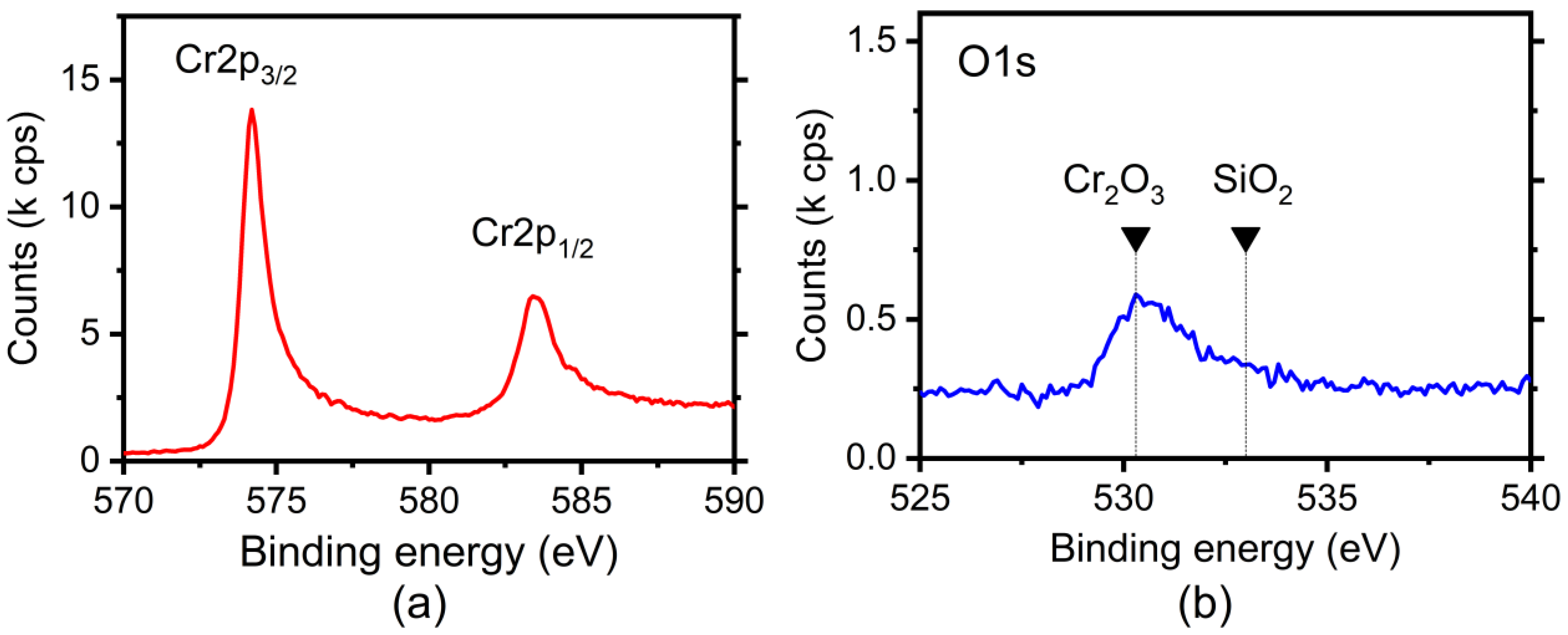
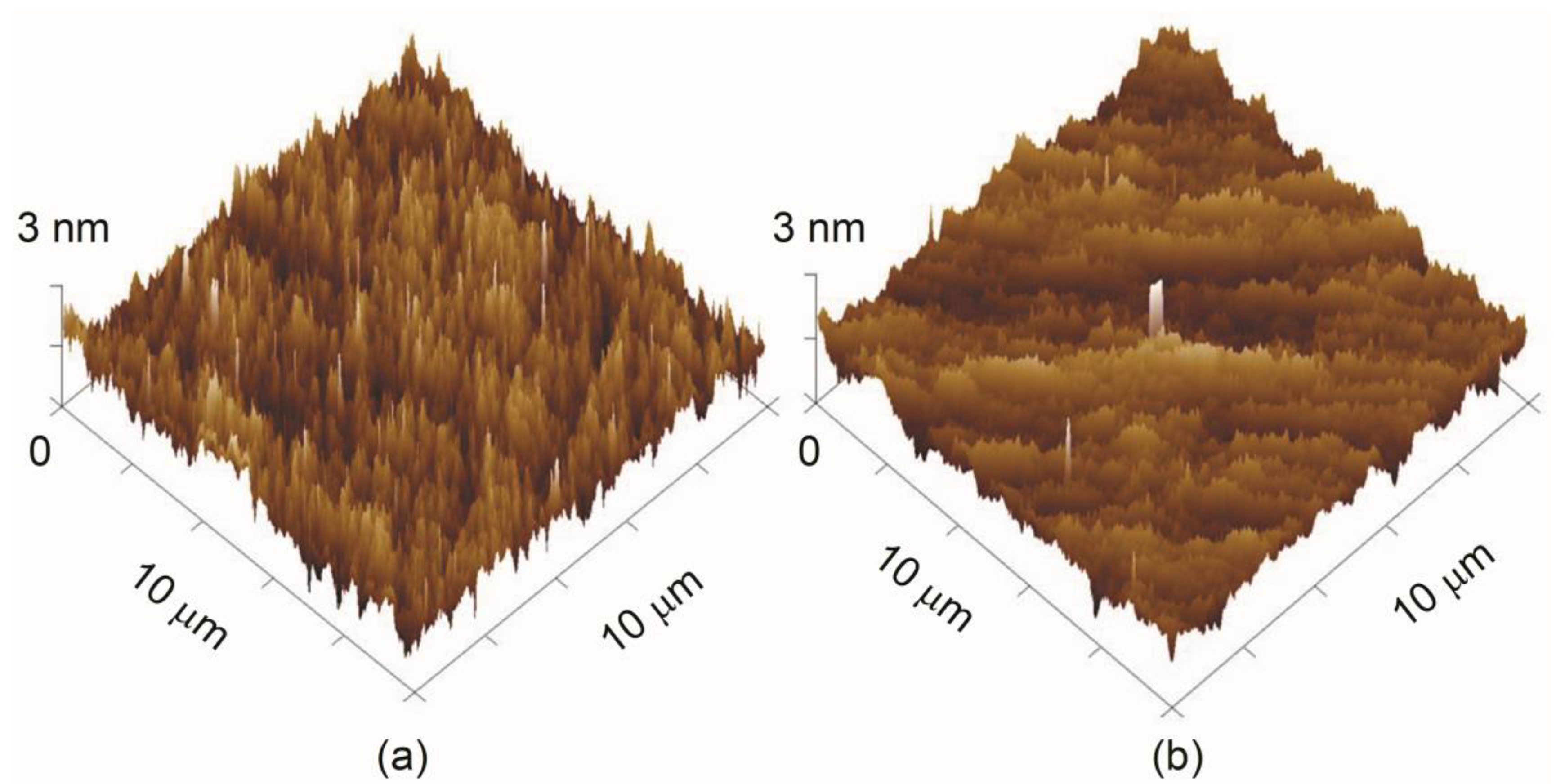
3.2. Surface Characteristics

The film morphology was analyzed by AFM, and Figure 3 illustrates a typical surface of continuous ultrathin chromium film. For the thinnest chromium film of 2.6 nm, the root mean square roughness (Rq) was determined to be 0.9 nm. Other films showed similar Rq values. Figure 3b presents the surface of 5 nm thick film with Rq of about 0.4 nm. The sharp peak seen in the middle of the sample was caused by the dust.
For a bare substrate, Rq varied in the range from 0.3 to 0.5 nm. A higher roughness of the 2.6 nm thick film might have been due to noncontinuous film morphology. However, starting from 5 nm thickness, our chromium films were totally continuous with a smooth surface morphology.
One of the advantages of Cr films is their low percolation threshold. Cr films on glassy substrates follow Stransky–Krastanov growth mode and hence become continuous much faster than, for example, Ag or Au films [40]. Similar AFM results for chromium films are reported, for example, in [41]. For the non-continuous film, the authors of that work were able to observe small uniform nanoparticles, while for continuous films, expanded smooth homogeneous structures were observed.

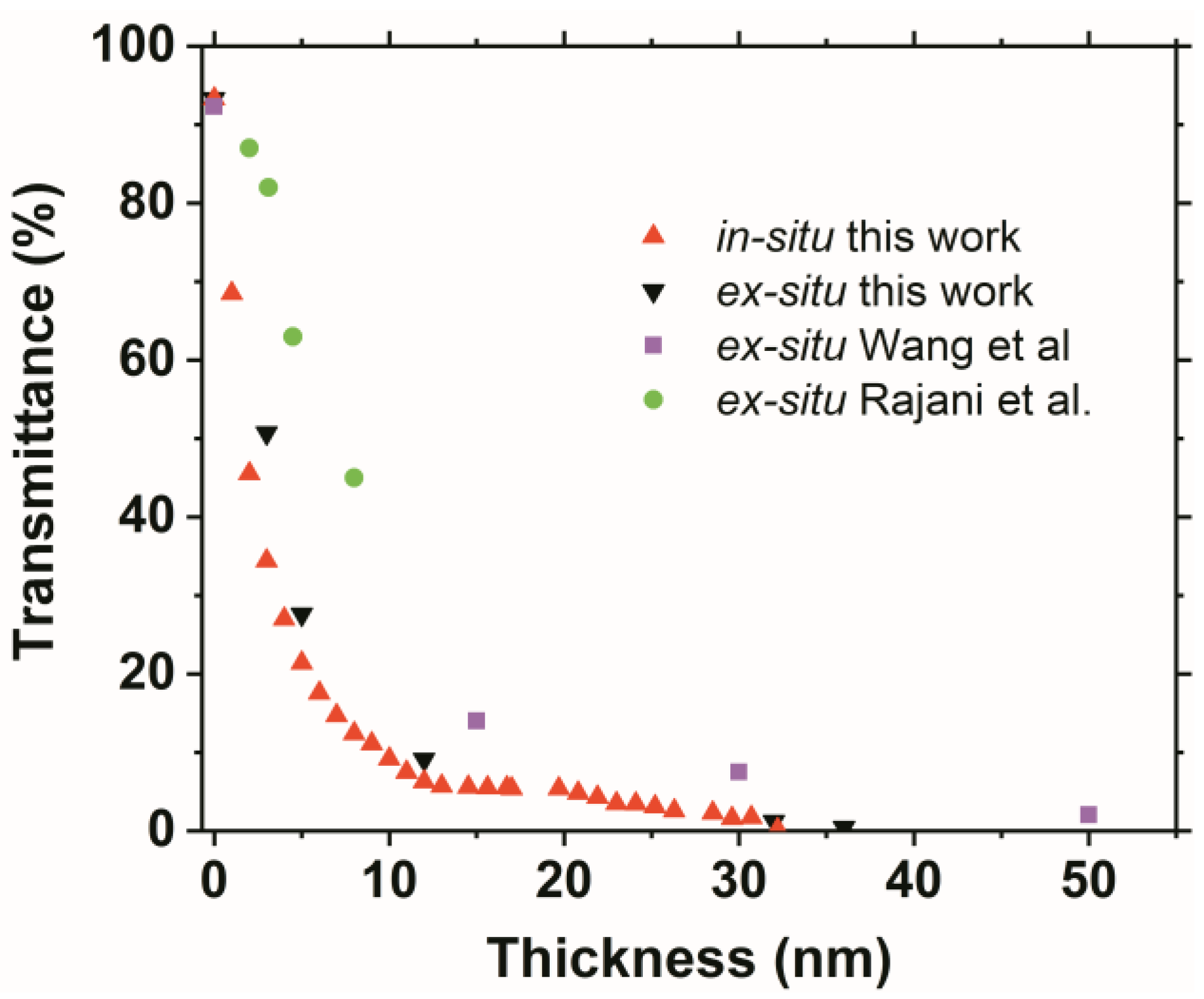
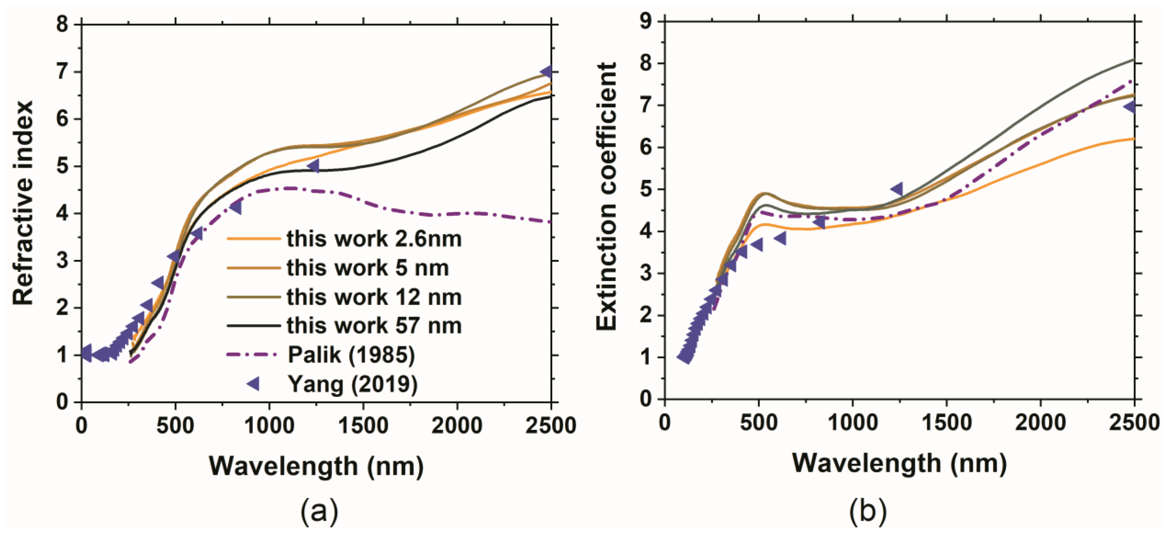
3.3. Optical Properties

The film transmittance spectra (Figure 4) were acquired in situ during the Cr film growth. In the investigated optical range, the transmittance changed monotonically. For comparison, in the case of Cu [42] or Ag [43] film growth, the transmittance evolution was different. The transmittance curves of the growing ultrathin Cu and Ag films exhibited plasmonic peaks at about 600 nm and 350 nm, respectively. Using monitoring of the transmittance curves, it is possible to deposit films with precise thickness, as reported in more detail in [42,43].
Figure 5 shows that the in situ and ex situ transmittance values did not differ significantly. This can be interpreted as an indirect proof of absence of significant surface oxidation. Our measurements follow the trend reported in the literature for magnetron-sputtered Cr films [3,18]. Slight difference in the results might be caused by a difference in the deposition conditions.
Figure 6 shows the transmittance spectra of the bare substrate and deposited Cr films in a broad wavelength range from the ultraviolet to the mid-infrared. The used substrates were transparent down to 5 µm, which limited the optical range of our investigation. The drops of transmission at 1300 nm and 2200 nm were due to substrate absorption.
Figure 7 shows the reflectance spectra of a bare substrate and of the samples with deposited Cr films. For the samples with thin metal films, the absorption peak corresponding to the substrate Si-O bond was clearly observable, and its intensity decreased with the film thickness. For the bare substrate and for some samples with the thinnest among the films in this study, the same absorption peak at 2.2 µm was clearly seen in the transmittance spectra (Figure 6). This peak almost completely disappeared for the films thicker than 27 nm, both in transmittance and reflectance spectra. The IR spectra did not show any characteristic absorption peaks of chromium oxide. Similar observations were reported, for example, by Cortazar-Martínez et al. [23].
The reflectance and transmittance values of thin Cr films may be tuned as required for an application by simply varying the film thickness, and the spectral response is relatively flat in a broad wavelength range. For example, for our sputtered films, the reflectance in the IR range may be tuned from 10% for an approximately 2.6 nm thick film up to 85% for a 57 nm thick film.
The optical constants of some selected sample are reported in Figure 8. The thickness value of the thinnest film is written with the first digit after the dot. Even a little change in thickness significantly influences the retrieved values of the optical constants for such films of a few nanometer thickness. Details on the optical characterization methodology and relevant discussion may be found in a dedicated paper [28]. Afterwards, these optical constants might be used for modelling multilayer metal-dielectric coatings [44,45].

3.4. Electrical Properties

The chromium film sheet resistance measurements are shown in Figure 9. In addition, a literature review was conducted to observe how different substrates and various deposition technologies influence the film sheet resistance. It is known that the sheet resistance is dependent on the binding force between the substrate and evaporated atoms. For example, an increase in the binding force may dramatically decrease sheet resistance [41].
Figure 8 illustrates the sheet resistance change during the film growth. The values had a similar trend compared with the literature data. Initially, the sheet resistance decreased with the thickness increase, and later on, the change was less significant. It should be noticed that the samples made by electron beam technique [2] showed the highest values of sheet resistance below 20 nm film thickness (5 nm–12,600 Ω/sq, 10 nm–2250 Ω/sq, 18 nm–1500 Ω/sq), while our chromium samples that were made by the pulsed DC magnetron sputtering technique showed the lowest values. These results are in good agreement with the pulsed DC magnetron-sputtered films reported previously [3]. In that article, the sheet resistance values corresponding to the 2, 3.1, 4.5, and 8 nm films were ≈5000, 1600, 400, and 100 Ω/sq, respectively. In our case, at 2.6 nm, chromium film’s sheet resistance was 981 Ω/sq, and it dramatically dropped to 164 Ω/sq (5 nm thickness), 54 Ω/sq (12 nm thickness), 12 Ω/sq (36 nm thickness), and 7 Ω/sq (57 nm thickness). This drop in sheet resistance can be explained by reduced scattering of free carriers on the grain boundaries between the crystallites. The stabilization of sheet resistance in our chromium samples started at 5 nm film thickness because the grain diameter started to be very large in comparison with the mean free path of conduction electrons [41].

4. Conclusions

Ultrathin chromium films were prepared by magnetron sputtering on fused silica substrates. The film growth and properties were investigated in situ and ex situ. The transmittance values measured in situ were very similar to the ex situ-measured values that showed no significant influence of exposure to the air. No significant oxidation was detected by XPS or FTIR measurements.
The reflectance and transmittance spectral curves were sufficiently flat in wide wavelength ranges, being useful for many optical applications where (almost) constant optical density is required. Thickness variation of the chromium film is a simple way to tune in a broad range their spectrally flat reflectance and transmittance. It was demonstrated that in situ control of the optical transmittance of the films is a reliable and precise method to regulate the thickness of the deposited ultrathin chromium film and finely tune its electrical and optical properties.

Author Contributions

Conceptualization, A.B. and A.S.; validation, A.B., A.S., K.B., V.V., V.J. and T.G.; formal analysis, A.B., A.S., K.B., V.V., V.J. and T.G.; investigation, A.B., A.S., K.B., V.V., V.J. and T.G.; resources, A.B.; writing—original draft preparation, A.B., A.S. and K.B.; writing—review and editing, A.B., A.S., K.B., V.V., V.J. and T.G.; resources A.B.; visualization, A.B. and K.B.; project administration, A.B.; funding acquisition, A.B. All authors have read and agreed to the published version of the manuscript.

Funding

This work was supported by the European Social Fund (project no. 09.3.3-LMT-K-712-19-0203) under a grant agreement with the Research Council of Lithuania (LMTLT).

Institutional Review Board Statement

Not applicable.

Informed Consent Statement

Not applicable.

Data Availability Statement

Not applicable.

Conflicts of Interest

The authors declare no conflict of interest.

References

  1. Ding, Y.; Zhang, F.; Yan, S.; Li, H.; He, J.; Yin, F. Microstructure, Micro-Indentation, and Scratch Behavior of Cr Films Prepared on Al alloys by Using Magnetron Sputtering. Metals 2019, 9, 1330. [Google Scholar] [CrossRef]
  2. Lozanova, V.; Lalova, A.; Soserov, L.; Todorov, R. Optical and electrical properties of very thin chromium films for optoelectronic devices. J. Phys. Conf. Ser. 2014, 514, 012003. [Google Scholar] [CrossRef]
  3. Rajani, K.V.; Daniels, S.; McNally, P.J.; Lucas, F.O.; Alam, M.M. Ultrathin chromium transparent metal contacts by pulsed dc magnetron sputtering. Phys. Status Solidi 2010, 207, 1586–1589. [Google Scholar] [CrossRef]
  4. Zervas, M.N. Surface plasmon–polariton waves guided by thin metal films. Opt. Lett. 1991, 16, 720–722. [Google Scholar] [CrossRef]
  5. Vial, A.; Laroche, T. Description of dispersion properties of metals by means of the critical points model and application to the study of resonant structures using the FDTD method. J. Phys. D Appl. Phys. 2007, 40, 7152–7158. [Google Scholar] [CrossRef]
  6. Hüger, E.; Dörrer, L.; Yimnirun, R.; Jutimoosik, J.; Stahn, J.; Paul, A. Lithium permeation within lithium niobate multilayers with ultrathin chromium, silicon and carbon spacer layers. Phys. Chem. Chem. Phys. 2018, 20, 23233–23243. [Google Scholar] [CrossRef]
  7. Norkus, M.; Skaudžius, R. Enhanced NIR Region Emission of Chromium by Changing the Chromium Concentration in Yttrium Aluminum Garnet (YAG) Host Matrix. J. Alloys Compd. 2022, 908, 164601. [Google Scholar] [CrossRef]
  8. Dhas, C.R.; Venkatesh, R.; Sivakumar, R.; Dhandayuthapani, T.; Subramanian, B.; Sanjeeviraja, C.; Raj, A.M.E. Electrochromic performance of chromium-doped Co3O4 nanocrystalline thin films prepared by nebulizer spray technique. J. Alloys Compd. 2019, 784, 49–59. [Google Scholar] [CrossRef]
  9. Shy, S.-L.; Lei, T.F.; Chu, C.H.; Chang, C.-Y.; Lee, S.H.; Loong, W.-A. Very Simple Data Processing System for Deep Submicron Nanofabrication. In Proceedings of the Electron-Beam, X-ray, and Ion-Beam Submicrometer Lithographies for Manufacturing IV, SPIE’s, 1994, Symposium on Microlitography, 27 February–4 March 1994, San Jose, CA, USA; Patterson, D., Ed.; SPIE: Bellingham, WA, USA, 1994; pp. 287–295. [Google Scholar] [CrossRef]
  10. Bloch, E.; Mistele, D.; Brener, R.; Cytermann, C.; Gavrilov, A.; Ritter, D. NiCr thin film resistor integration with InP technology. Semicond. Sci. Technol. 2011, 26, 105004. [Google Scholar] [CrossRef]
  11. Miller, R.; Holland, H. Crystallographic orientation of sputtered Cr films on glass and glass–ceramic substrates. Thin Solid Films 1997, 298, 182–186. [Google Scholar] [CrossRef]
  12. Chiang, K.-T.K.; Wei, R. Growth morphology and corrosion resistance of magnetron sputtered Cr films. Surf. Coatings Technol. 2011, 206, 1660–1665. [Google Scholar] [CrossRef]
  13. Kashkarov, E.; Sidelev, D.; Rombaeva, M.; Syrtanov, M.; Bleykher, G. Chromium coatings deposited by cooled and hot target magnetron sputtering for accident tolerant nuclear fuel claddings. Surf. Coatings Technol. 2020, 389, 125618. [Google Scholar] [CrossRef]
  14. Chen, N.; Chen, L.; Li, Y.; Li, W.; Zhao, Y.; Wang, Z.; Wang, X.; Bu, Y. Design and fabrication of metameric interference thin films based on metal-dielectric structure for optical security devices. Surf. Coatings Technol. 2019, 364, 392–397. [Google Scholar] [CrossRef]
  15. Lunk, H.-J. Discovery, properties and applications of chromium and its compounds. ChemTexts 2015, 1, 6. [Google Scholar] [CrossRef]
  16. Wang, Z.-Y.; Hu, E.-T.; Cai, Q.-Y.; Wang, J.; Tu, H.-T.; Yu, K.-H.; Chen, L.-Y.; Wei, W. Accurate Design of Solar Selective Absorber Based on Measured Optical Constants of Nano-thin Cr Film. Coatings 2020, 10, 938. [Google Scholar] [CrossRef]
  17. Rahimi, H.; Karimi, M.; Ghajarpour-Nobandegani, S. Chromium nanostructures for enhancing light trapping in a thin-film solar cell. Opt. Mater. 2021, 121, 111548. [Google Scholar] [CrossRef]
  18. Wang, S.-F.; Lin, H.-C.; Bor, H.-Y.; Tsai, Y.-L.; Wei, C.-N. Characterization of chromium thin films by sputter deposition. J. Alloys Compd. 2011, 509, 10110–10114. [Google Scholar] [CrossRef]
  19. Ferreira, A.A.; Silva, F.J.G.; Pinto, A.G.; Sousa, V.F.C. Characterization of Thin Chromium Coatings Produced by PVD Sputtering for Optical Applications. Coatings 2021, 11, 215. [Google Scholar] [CrossRef]
  20. Kim, T.J.; Thio, T.; Ebbesen, T.W.; Grupp, D.E.; Lezec, H.J. Control of optical transmission through metals perforated with subwavelength hole arrays. Opt. Lett. 1999, 24, 256–258. [Google Scholar] [CrossRef]
  21. Mroczyński, R.; Iwanicki, D.; Fetliński, B.; Ożga, M.; Świniarski, M.; Gertych, A.; Zdrojek, M.; Godlewski, M. Optimization of Ultra-Thin Pulsed-DC Magnetron Sputtered Aluminum Films for the Technology of Hyperbolic Metamaterials. Crystals 2020, 10, 384. [Google Scholar] [CrossRef]
  22. Grilli, M.L.; Vernhes, R.; Hu, G.; Di Sarcina, I.; Dikonimos, T.; Sytchkova, A.; Martinu, L.; He, H.; Piegari, A. Characteristics of Ultrathin Ni Films. Phys. Status Solidi 2019, 216, 1800728. [Google Scholar] [CrossRef]
  23. Cortazar-Martínez, O.; Torres-Ochoa, J.-A.; Raboño-Borbolla, J.-G.; Herrera-Gomez, A. Oxidation mechanism of metallic chromium at room temperature. Appl. Surf. Sci. 2021, 542, 148636. [Google Scholar] [CrossRef]
  24. Safi, I. Recent aspects concerning DC reactive magnetron sputtering of thin films: A review. Surf. Coatings Technol. 2000, 127, 203–218. [Google Scholar] [CrossRef]
  25. Musil, J.; Baroch, P.; Vlček, J.; Nam, K.; Han, J. Reactive magnetron sputtering of thin films: Present status and trends. Thin Solid Films 2005, 475, 208–218. [Google Scholar] [CrossRef]
  26. Anders, A. Tutorial: Reactive high power impulse magnetron sputtering (R-HiPIMS). J. Appl. Phys. 2017, 121, 171101. [Google Scholar] [CrossRef]
  27. Greene, J.E. Tracing the recorded history of thin-film sputter deposition: From the 1800s to 2017. J. Vac. Sci. Technol. A Vac. Surf. Film. 2017, 35, 05C204. [Google Scholar] [CrossRef]
  28. Sytchkova, A.; Belosludtsev, A.; Volosevičienė, L.; Juškėnas, R.; Simniškis, R. Structural, optical and electrical properties of sputtered ultrathin chromium films. Opt. Mater. 2021, 121, 111530. [Google Scholar] [CrossRef]
  29. Wu, W.-Y.; Hsiao, B.-H.; Chen, P.-H.; Chen, W.-C.; Ho, C.-T.; Chang, C.-L. CrNx films prepared using feedback-controlled high power impulse magnetron sputter deposition. J. Vac. Sci. Technol. A Vac. Surf. Film. 2014, 32, 02B115. [Google Scholar] [CrossRef]
  30. Bryan, H.A.; Dean, J.A. Extraction and Flame Spectrophotometric Determination of Chromium. Anal. Chem. 1957, 29, 1289–1292. [Google Scholar] [CrossRef]
  31. Šlapanská, M.; Hecimovic, A.; Gudmundsson, J.T.; Hnilica, J.; Breilmann, W.; Vašina, P.; von Keudell, A. Study of the transition from self-organised to homogeneous plasma distribution in chromium HiPIMS discharge. J. Phys. D Appl. Phys. 2020, 53, 155201. [Google Scholar] [CrossRef]
  32. de Monteynard, A.; Schuster, F.; Billard, A.; Sanchette, F. Properties of chromium thin films deposited in a hollow cathode magnetron powered by pulsed DC or HiPIMS. Surf. Coat. Technol. 2017, 330, 241–248. [Google Scholar] [CrossRef]
  33. Song, L.; Mazumder, J. Real Time Cr Measurement Using Optical Emission Spectroscopy During Direct Metal Deposition Process. IEEE Sens. J. 2011, 12, 958–964. [Google Scholar] [CrossRef]
  34. Benien, H.; Maushart, J.; Meyer, M.; Suchentrunk, R.D.c. magnetron sputtering of oxidation-resistant chromium and CrN films monitored by optical emission spectrometry. Mater. Sci. Eng. A 1991, 139, 126–131. [Google Scholar] [CrossRef]
  35. Siepa, S.; Danko, S.; Tsankov, T.V.; Mussenbrock, T.; Czarnetzki, U. On the OES line-ratio technique in argon and argon-containing plasmas. J. Phys. D Appl. Phys. 2014, 47, 445201. [Google Scholar] [CrossRef]
  36. Tam, P.; Cao, Y.; Nyborg, L. Thin film characterisation of chromium disilicide. Surf. Sci. 2013, 609, 152–156. [Google Scholar] [CrossRef]
  37. Musil, J.; Zenkin, S.; Kos, S.; Čerstvý, R.; Haviar, S. Flexible hydrophobic ZrN nitride films. Vacuum 2016, 131, 34–38. [Google Scholar] [CrossRef]
  38. Belosludtsev, A.; Houška, J.; Vlček, J.; Haviar, S.; Čerstvý, R.; Rezek, J.; Kettner, M. Structure and properties of Hf-O-N films prepared by high-rate reactive HiPIMS with smoothly controlled composition. Ceram. Int. 2017, 43, 5661–5667. [Google Scholar] [CrossRef]
  39. Houska, J.; Kozak, T. Distribution of O atoms on partially oxidized metal targets, and the consequences for reactive sputtering of individual metal oxides. Surf. Coatings Technol. 2020, 392, 125685. [Google Scholar] [CrossRef]
  40. Kaiser, N. Review of the fundamentals of thin-film growth. Appl. Opt. 2002, 41, 3053–3060. [Google Scholar] [CrossRef]
  41. Lovrinčić, R.; Pucci, A. Infrared optical properties of chromium nanoscale films with a phase transition. Phys. Rev. B 2009, 80, 205404. [Google Scholar] [CrossRef]
  42. Belosludtsev, A.; Kyžas, N. Real-time in-situ investigation of copper ultrathin films growth. Mater. Lett. 2018, 232, 216–219. [Google Scholar] [CrossRef]
  43. Belosludtsev, A.; Sytchkova, A.; Kyžas, N.; Bitinaitis, I.; Simniškis, R.; Drazdys, R. Comparison of in-situ investigation of silver ultrathin films growth with the ex-situ resistance and ellipsometric measure-ments. Vacuum 2021, 195, 110669. [Google Scholar] [CrossRef]
  44. Kar, C.; Jena, S.; Udupa, D.V.; Rao, K.D. Tamm plasmon polariton in planar structures: A brief overview and applications. Opt. Laser Technol. 2023, 159, 108928. [Google Scholar] [CrossRef]
  45. Vyunishev, A.M.; Bikbaev, R.G.; Svyakhovskiy, S.E.; Timofeev, I.V.; Pankin, P.S.; Evlashin, S.A.; Vetrov, S.Y.; Myslivets, S.A.; Arkhipkin, V.G. Broadband Tamm plasmon polariton. J. Opt. Soc. Am. B 2019, 36, 2299–2305. [Google Scholar] [CrossRef]
  46. Lin, J.; Lin, L.; Guan, G.; Wu, Y.; Lai, F. Structural, Optical and Electrical Properties of Chromium Thin Films Prepared by Magnetron Sputtering. Guangzi Xuebao/Acta Photonica Sin. 2012, 41, 922–926. [Google Scholar] [CrossRef]
  47. Udachan, S.L.; Ayachit, N.H.; Udachan, L.A. Impact of substrates on the electrical properties of thin chromium films. Ing. Y Univ. 2019, 23, 1–19. [Google Scholar] [CrossRef]
Figure 1. Optical emission spectra of Cr plasma. The most intensive Cr emission and Ar emission lines are indicated.
Coatings 13 00347 g001
Figure 2. The high-resolution Cr2p (a) and O1s (b) XPS spectra for Cr ultrathin film.
Coatings 13 00347 g002
Figure 3. Three-dimensional AFM surface images of Cr film with thicknesses of 3 nm (a) and 5 nm (b).
Coatings 13 00347 g003
Figure 4. In situ transmittance evolution during Cr film growth.
Coatings 13 00347 g004
Figure 5. Evolution of the transmittance values at 550 nm wavelength extracted from the spectral data acquired during Cr film growth. The in situ and ex situ data of this study (triangles) are plotted in comparison with ex situ data by Wang [18] (squares) and Rajani [3] (circles).
Coatings 13 00347 g005
Figure 6. Ex situ UV-visible IR transmittance of bare fused silica substrate and of the samples with deposited Cr films of various thicknesses.
Coatings 13 00347 g006
Figure 7. Ex situ UV-visible IR reflectance of bare fused silica substrate and of the samples with deposited Cr films of various thicknesses.
Coatings 13 00347 g007
Figure 8. The optical constants of Cr films: (a) refractive index and (b) extinction coefficient.
Coatings 13 00347 g008
Figure 9. Sheet resistance change during the Cr film growth obtained in our experiments in comparison with the literature data [2,3,46,47].
Coatings 13 00347 g009
Disclaimer/Publisher’s Note: The statements, opinions and data contained in all publications are solely those of the individual author(s) and contributor(s) and not of MDPI and/or the editor(s). MDPI and/or the editor(s) disclaim responsibility for any injury to people or property resulting from any ideas, methods, instructions or products referred to in the content.

