Probing the Field-Effect Transistor with Monolayer MoS2 Prepared by APCVD


Key Laboratory for Wide-Band Gap Semiconductor Materials and Devices of Education, The School of Microelectronics, Xidian University, Xi’an 710071, China
*
Authors to whom correspondence should be addressed.
Nanomaterials 2019, 9(9), 1209; https://doi.org/10.3390/nano9091209
Submission received: 25 July 2019
/
Revised: 13 August 2019
/
Accepted: 22 August 2019
/
Published: 27 August 2019
Abstract
:The two-dimensional materials can be used as the channel material of transistor, which can further decrease the size of transistor. In this paper, the molybdenum disulfide (MoS2) is grown on the SiO2/Si substrate by atmospheric pressure chemical vapor deposition (APCVD), and the MoS2 is systematically characterized by the high-resolution optical microscopy, Raman spectroscopy, photoluminescence spectroscopy, and the field emission scanning electron microscopy, which can confirm that the MoS2 is a monolayer. Then, the monolayer MoS2 is selected as the channel material to complete the fabrication process of the back-gate field effect transistor (FET). Finally, the electrical characteristics of the monolayer MoS2-based FET are tested to obtain the electrical performance. The switching ratio is 103, the field effect mobility is about 0.86 cm2/Vs, the saturation current is 2.75 × 10⁻⁷ A/μm, and the lowest gate leakage current is 10−12 A. Besides, the monolayer MoS2 can form the ohmic contact with the Ti/Au metal electrode. Therefore, the electrical performances of monolayer MoS2-based FET are relatively poor, which requires the further optimization of the monolayer MoS2 growth process. Meanwhile, it can provide the guidance for the application of monolayer MoS2-based FETs in the future low-power optoelectronic integrated circuits.
1. Introduction
The field effect transistors (FETs) are the basic unit of very large scale integrated circuits [1,2]. The feature size of the transistor has reached the physical limit with the integration of integrated circuits increases. Therefore, it is necessary to find the suitable semiconductor materials to improve the electrical performance of transistor [3,4]. Many researchers have focused on the two-dimensional materials with the single layer of atomic thickness [5]. The two-dimensional material is used as the channel material compared to the traditional bulk material, which can not only help to suppress the short channel effect, but also effectively reduces the static leakage current [6,7]. In addition, the two-dimensional materials also have the higher specific surface area, excellent mechanical strength, higher optical transparency, and various excellent photoelectric characteristics, so it can be widely used in the gas sensors [8], flexible electronics [9], and photodetectors [10]. Compared to the Si material, there are no dangling bonds in the low-dimensional transition metal sulfur compound materials when the transistor size is at the zoom limit [11]. The molybdenum disulfide (MoS2) has the semiconductor characteristics, excellent physical and chemical properties, and unique microstructure, which can directly construct the field effect transistor. Therefore, the MoS2 has become the very promising channel material in the process of the transistor scale.
As we all know, the thickness of the MoS2 sample obtained by the mechanical peeling is larger, and the MoS2 sample is smaller and irregular, so the MoS2 is grown on the SiO2/Si substrate by the atmospheric pressure chemical vapor deposition (APCVD) [12]. There are many factors that affect the continuity and uniformity of the MoS2 deposition while using the APCVD method to obtain the MoS2, such as the growth temperature, growth time, the amount of S powder and MoO3 powder, and the gas flow rate. The band gap of MoS2 changes with the number of layers, the bulk MoS2 has the moderate electron mobility and an indirect band gap of 1.29 eV, whereas the monolayer MoS2 is a direct bandgap material with a band gap of 1.8 eV. The MoS2 is a promising material for the flexible and transparent substrates, which can be applied in the logic circuits and optoelectronic devices [13]. The size and quality of MoS2 have a great influence on the performance of the device. Therefore, we can improve the continuity and uniformity of the MoS2 deposition by adjusting the growth process parameters and treating the SiO2/Si substrate with the graphene quantum dot solution [14]. The FETs with the direct bandgap monolayer MoS2 have the larger switching ratio and the lower off-state current. However, the mobility and on-state current of the FETs are very lower, so it is very meaningful to optimize and enhance the electrical performance, which can provide the application reference of the monolayer MoS2-based FETs.
The paper is composed of five parts: First, the large-area high-quality monolayer MoS2 is prepared by the APCVD to facilitate the fabrication of FETs [15]. Then, the monolayer MoS2 is confirmed and characterized by the high resolution microscopy, Raman spectroscopy, photoluminescence spectroscopy, and field emission scanning electron microscopy. Next, the main preparation process of monolayer MoS2-based FET is described. Subsequently, the electrical performance of the back-gate FET is measured. Finally, the conclusion of this paper is summarized. The following are the electrical performance parameters of the prepared monolayer MoS2-based FET in this paper, the electrical performance parameters have increased by improving the electrode contact and channel material [16]. The switching ratio is as high as 103, the field effect mobility is about 0.86 cm2/Vs, the saturation current is 2.75 × 10⁻⁷ A/μm, and the lowest gate leakage current is 10−12 A. Besides, the monolayer MoS2 can form the ohmic contact with the Ti/Au electrode. Although the electrical performance of monolayer MoS2-based FETs is not ideal, we have mastered the fabrication process of monolayer MoS2-based FETs, and the growth process of monolayer MoS2 needs further optimization, which can provide the reference for the preparation of high quality monolayer MoS2-based FETs [17].
2. The Growth and Characterization of Monolayer MoS2
2.1. The Growth Process of Monolayer MoS2
In this paper, the monolayer MoS2 on SiO2/Si substrate was grown by APCVD. First, the solid sulfur powder and MoO3 powder could be melted into the gas state under the high temperature. Then the argon gas with a purity of 99.999% was passed as the carrier gas, and the sulfur gas was transferred to the vicinity of the SiO2/Si substrate. At the same time, there was a certain concentration of MoO3 vapor in the vicinity of the SiO2/Si substrate. Finally, the sulfur gas could react with MoO3 gas on the surface of the SiO2/Si substrate to form the MoS2. The specific growth experiment process of monolayer MoS2 was as follows: The SiO2/Si substrate was selected as the growth substrate of MoS2, wherein 300 nm SiO2 was the back gate dielectric layer of FET [18]. Before the growth experiment of MoS2, the 1 cm × 1 cm SiO2/Si substrate was first subjected to the oxygen plasma treatment. The vacuum tube furnace of the MoS2 growth experiment was TF55035C-1, and the front end is equipped with a heater that could be heated to 400 °C, which could help to assist the evaporation of sulfur powder. First, the quartz boat with 100 ± 5 mg sulfur powder (Alfa Aesar, Shanghai, China, 99.5%) was placed in the middle zone of the heater. Then, the quartz boat with 2 ± 0.1 mg MoO3 powder (Alfa Aesar, Shanghai, China, 99.95%) and SiO2/Si substrate was placed in the middle of the tube furnace. Next, the argon gas with 200 sccm was introduced into the tube furnace for 10 min to eliminate the air of the tube furnace. Subsequently, the temperature of the sulfur powder was heated to 200 °C, and the MoO3 powder was heated to 750 °C. During the growth of MoS2, the argon gas with a flow rate of 40 sccm was continuously provided and the growth temperature was maintained for 10 min [19]. Finally, the growth reaction of MoS2 was completed, and the MoS2 sample was taken out while the temperature of the tube furnace was cooled to room temperature.
2.2. The Test Characterization Conditions of Monolayer MoS2
The MoS2 sample could be obtained by the APCVD. At the same time, the MoS2 could be systematically characterized by optical microscopy, Raman spectroscopy, photoluminescence spectroscopy, and field emission scanning electron microscopy to further determine the layer number and quality of the MoS2 sample. The Raman model was LabRam HR Evolution with a laser wavelength of 532 nm (HORIBA JobinYvon, Paris, France) [20]. The specific test conditions of the Raman spectrometer were the 100× objective lens, 1800 groove/mm grating, the spot size of 532 nm laser was 342 nm, and the incident laser power density was 140 μW/μm2. Besides, the field emission scanning electron microscopy (FESEM, JSM-6700F, Hitachi, Tokyo, Japan) was also used at the accelerating voltage of 5 kV.
The monolayer MoS2 and the SiO2 of SiO2/Si substrate could interfere with the light, so there was a reflection enhancement effect on the visible light wavelength of 532 nm. Figure 1a,b respectively show the 50× and 100× objective optical micrograph of monolayer MoS2, the pink and blue patches in the optical images respectively represents the monolayer MoS2 on SiO2/Si substrate and the scale, it could be observed by the optical microscope that monolayer MoS2 on SiO2/Si substrate exhibited the bright blue color. As shown in Figure 1c, the typical FESEM image of monolayer MoS2 clearly exhibited the quasi-equilateral triangles, which was consistent with the crystal structure. Besides, the Raman mapping was tested to observe the film formation quality and uniformity of the triangular MoS2. It can be seen from the Figure 1d that the color of MoS2 mapping was relatively uniform, which could indicate that the sample was the high-quality uniform monolayer MoS2.
There were two characteristic peaks in the Raman spectrum of MoS2, the layer number of MoS2 sample could be measured by the Raman spectrum between the E12g mode and the A1g mode. It could be found by observing Figure 2a that the distance Δk between the E12g characteristic peak and A1g characteristic peak was 18 ± 0.1 cm−1, and the ratio of A1g/E12g was about 1.043, which indicates that the MoS2 sample was a monolayer [21]. Figure 2b shows the photoluminescence spectrum of the monolayer MoS2 sample at different points. The photoluminescence spectrum of monolayer MoS2 on SiO2/Si substrate had I and B exciton peaks, the strongest I exciton peak position of monolayer MoS2 was at 684.6 ± 0.5 nm, which could be explained by the direct exciton excitation [22]. The corresponding electron volt was at 1.82 ± 0.02 eV through the conversion relationship between wavelength and electron volts, which was consistent with the direct band gap width of monolayer MoS2. In addition, there was also the B exciton peak at 1.97 ± 0.02 eV due to the 3d orbital electron interaction of Mo atoms, which could further prove that the sample was the large-area high-quality monolayer MoS2.
In Figure 2c, the Raman spectrum intensity of monolayer MoS2 increased with the laser power increase. There was a blue shift of the E12g characteristic peak when the laser power increased, and the A1g characteristic peak position did not change. This was because the MoS2 on the SiO2/Si substrate was an n-type doped semiconductor material [23]. Figure 2d shows the power photoluminescence spectrum of monolayer MoS2. The peak intensity of the photoluminescence spectrum increased when the laser power increased. At the same time, the relative positions between the I exciton peak and B exciton peak were red-shifted to some extent when the laser power increased. The reason was that the MoS2 on SiO2/Si substrate was the n-type doped material [24]. It is known from the above Raman spectrum and photoluminescence spectrum that the MoS2 sample was a monolayer.
3. The Discussion of Electrical Performance Results
The field effect transistor is the most basic electronic component in the digital logic circuits, which consists of the channel, a source electrode, a drain electrode, and the gate dielectric layer [25]. It can control the channel internal carrier density and the source–drain current by adjusting the gate voltage, which can achieve the current amplification and power amplification.
3.1. The Fabrication Process of Monolayer MoS2-Based FET
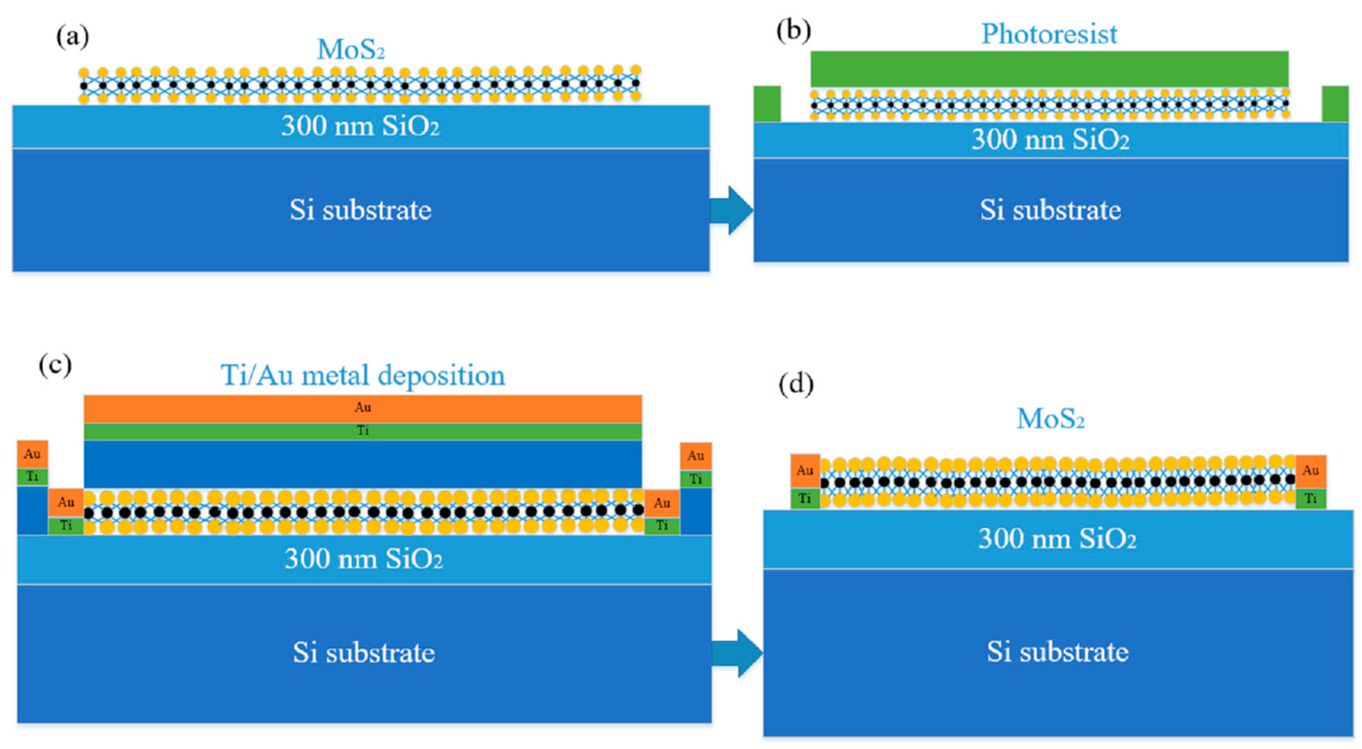
The monolayer MoS2-based back-gate FET can be fabricated by the photolithography, electron beam evaporation, and lift-off micromachining processes, the above steps used the polymethyl methacrylate (PMMA) resist process. The following is the specific process flow schematic diagram of monolayer MoS2-based FET [26]. First, the high-quality triangular monolayer MoS2 is grown on the surface of Si/SiO2 substrate by APCVD, as shown in Figure 3a; in Figure 3b, the pre-baking, gluing, exposing, and developing processes were performed to complete the photolithography, then using the photoresist as a mask, and the Ar plasma etching process was performed to remove the exposed MoS2 film, the photoresist was removed by the acetone solution, the ethanol solution was cleaned to determine the source and drain windows of monolayer MoS2-based FET; Subsequently, the 20 nm Ni/70 nm Au were used as the source-drain metal contact by the electron beam evaporation, as shown in Figure 3c; Next, the photoresist was dissolved in the acetone solution, and the metal solution was removed by the ethanol solution, as shown in Figure 3d.
Finally, the device was annealed in the vacuum environment of 180 °C for 2 h to remove the photoresist residue and decrease the contact resistance between the Ti/Au metal and monolayer MoS2. The fabrication of monolayer MoS2-based FET was completed, and the electrical performance of monolayer MoS2-based FET was analyzed and tested by the multi-function probe station and the B1500A semiconductor parameter analyzer (Santa Clara, CA, USA).
Figure 4a–c respectively show the 10×, 50×, and 100× objective optical microscope images of the monolayer MoS2-based back-gate FET, and the pink and blue patches in the optical images respectively represents the monolayer MoS2 on SiO2/Si substrate and the scale, it can be found that the area of monolayer MoS2 was usually 10–30 μm, and the size of the triangular monolayer MoS2 was relatively smaller compared to the metal electrodes, so the source and drain metal electrodes were divided into an electrode lead and the pad. The electrode lead (line width of 5 μm) was directly in contact with monolayer MoS2, and the pad of the source and drain metal electrodes was a square of 100 μm × 100 μm, which was for the electrical performance tests on the multi-function probe station [27]. The FESEM image of the monolayer MoS2-based back-gate FET is given in Figure 4d, it can be seen that the uneven brightness and blurred focus appeared on the surface of monolayer MoS2, which was affected by the charging effect of the SiO2/Si substrate during the FESEM scanning.
3.2. The Electrical Properties of Monolayer MoS2-Based FET
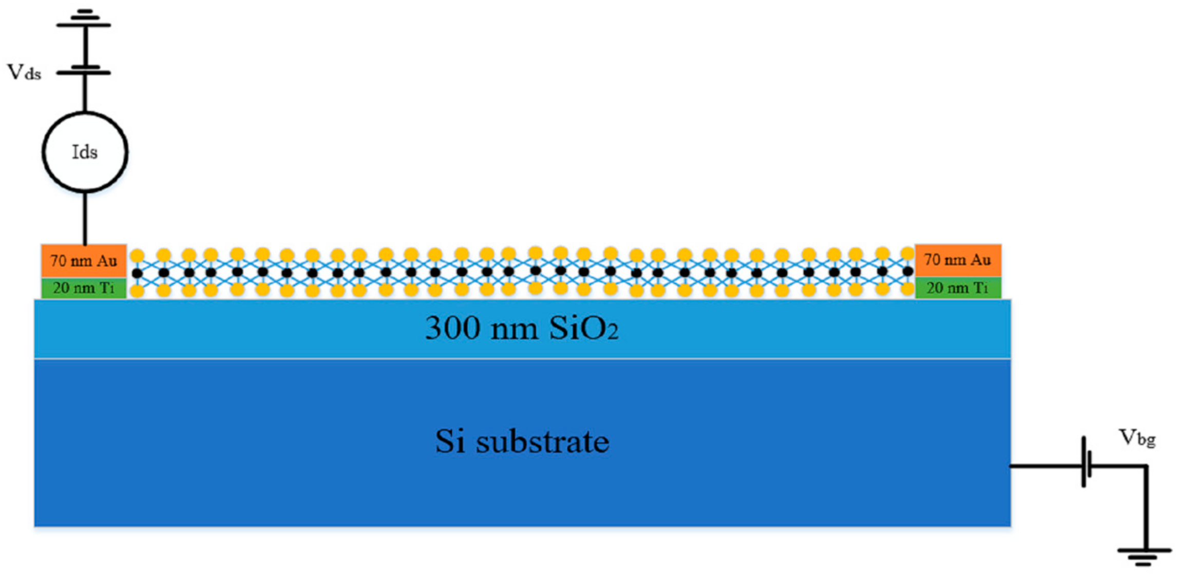
Figure 5 shows the electrical test structure schematic diagram of the monolayer MoS2-based back-gate FET. The gate oxide of the back gate electrode was 300 nm SiO2, and monolayer MoS2 was used as the conductive channel material. To decrease the contact resistance, the source/drain metal electrodes were made of 20 nm Ti/70 nm Au. The 20 nm Ti metal acted as the adhesion layer between monolayer MoS2 and the Au, which could prevent the Au metal falling off from the MoS2 film [28]. Besides, the Ti metal could also facilitate the formation of the ohmic contact between the monolayer MoS2 sample and the Au electrode.
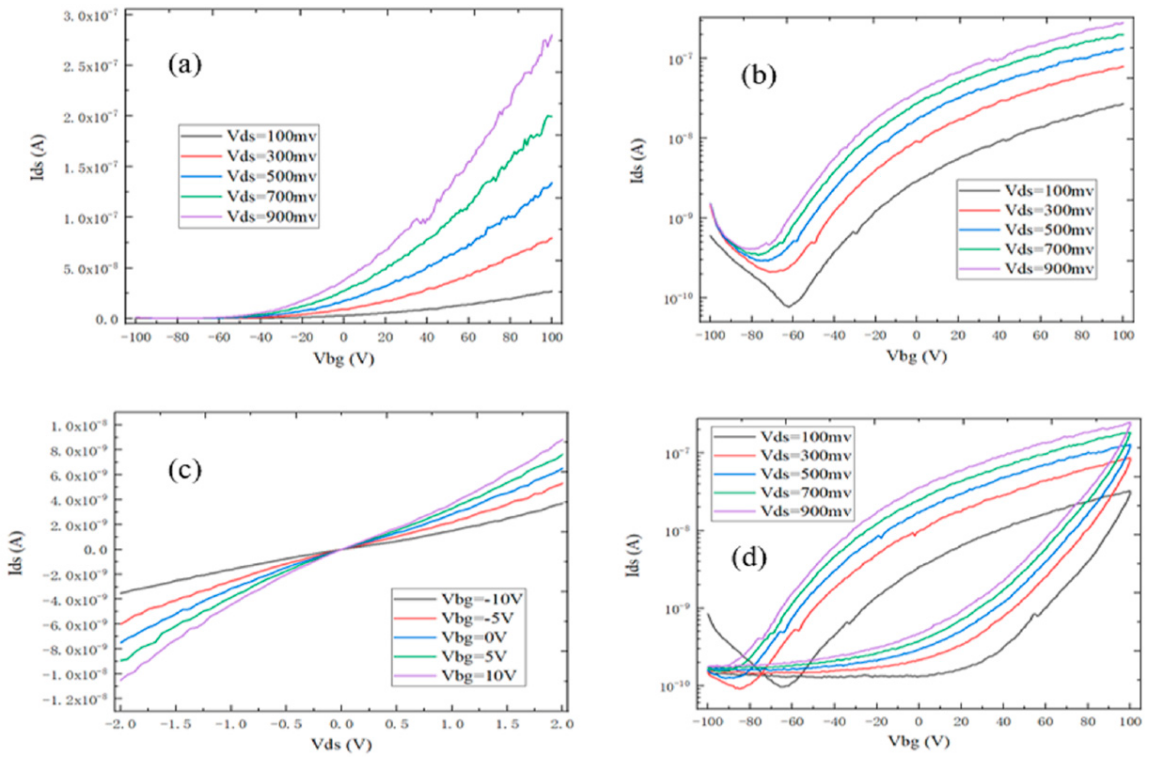
The transfer and output characteristics of monolayer MoS2-based back-gate FET are shown in Figure 6. It can be seen by observing Figure 6a that the on-state current of the FET increased with the source–drain voltage increase. When the source–drain voltage was 0.9 V, the on-state current was about 2.75 × 10⁻⁷ A/μm, which was far from the application requirement of the high-performance FET [29]. In Figure 6b, the gate voltage could effectively regulate the channel resistance and the source-drain current, which exhibited the better switching characteristics. The source–drain current decreased when the back-gate electrode was at the negative voltage, whereas the source–drain current increased when a forward voltage was applied to the back-gate electrode, so the monolayer MoS2-based FET was the n-type transmission, and the switching ratio could reach 103. The reason was that monolayer MoS2 had the smaller grain size and the relatively poor quality, which had a major effect on the device performance.
Based on the Ids–Vgs transfer curve, the field effect mobility can be calculated by using the following equation [30]:
The channel length of device L = 10 μm, the channel width of device W = 10 μm, the source and drain voltage Vds = 0.9 V, vacuum dielectric constant ε0 = 8.85 × 10⁻¹² F/m, the relative dielectric constant of SiO2 εr = 3.9, the thickness of SiO2 d = 300 nm, dIds/dVgs is the slope of the transfer curve. Therefore, when the Vds is 0.9 V, the field effect mobility is approximately 0.86 ± 0.05 cm2/Vs according to the slope of the linear region between 40 V and 100 V. This is because the lattice structure of MoS2 grown by APCVD is not complete. There are the lattice defects, which can deteriorate the mobility of monolayer MoS2-based FET. Due to the large forbidden band width of monolayer MoS2, the lowest gate leakage current of MoS2 FET is at the 10−12 A when the gate voltage gradually increase from −100 to 100 V, so it is suitable for the low-power logic circuits. The lower gate leakage current can effectively decrease the leakage power, which can help to improve the lifetime of the device [31]. As shown in Figure 6c, the output curve of monolayer MoS2 FET was linear, the gate voltage could well control the output current, and the output current increased with the gate voltage increase, which indicates that the monolayer MoS2-based FET was an n-type carrier transmission. For the monolayer MoS2-based back-gate FET, the current was proportional to Vds in the linear regime at the small source-drain voltage, and the Ids–Vds curve of FET device exhibited the odd function characteristic with the good linearity and central symmetry when the Vds increased from −2 to 2 V. Moreover, the Vgs had a significant regulation effect on the slope of the output curve, which indicates that the monolayer MoS2-based back gate FET could form the good ohmic contact between the Ti/Au metal and MoS2 channels. It can be found from Figure 6d that the transfer characteristic curve had the obvious hysteresis phenomenon. This is due to the fact that the channel material used monolayer MoS2, which was very sensitive to the environmental change [32]. The monolayer MoS2-based FET could absorb the moisture and impurity gases from the air, which would have the important impact on the electrical performance of the monolayer MoS2-based FET.
4. Conclusions
In this paper, the monolayer MoS2 on SiO2/Si substrate was grown by APCVD, and the MoS2 sample was characterized by the high resolution microscope, the Raman spectroscopy, photoluminescence spectroscopy, and field emission scanning electron microscopy, which could prove the existence of monolayer MoS2. In order to evaluate the quality of monolayer MoS2 systematically, the monolayer MoS2 was used as the channel material of the FET, and the back gate FET was fabricated on the monolayer MoS2. It could be found from the electrical parameters of FET that the ohmic contact could be formed between monolayer MoS2 and Ti/Au metal electrode, the gate leakage current and static power consumption were lower. At the same time, the on-state current was about 2.75 × 10⁻⁷ A/μm when the source-drain voltage was 0.9 V, both the switching ratio and the mobility increased to some extent, which still need further improvement. The growth process of MoS2 was optimized to obtain the higher quality monolayer MoS2, so that the monolayer MoS2-based FET could be applied to the future low-power optoelectronic integrated circuits.
Author Contributions
Conceptualization and writing—original draft preparation, T.H. and K.Y.; methodology, S.W. and S.C.; validation, T.H. and H.X.; writing—review and editing, H.L. and S.W.; funding acquisition, H.L.
Funding
This research was funded by the National Natural Science Foundation of China (Grant Nos. U1866212 and 61904136), the Foundation for Fundamental Research of China (Grant No. JSZL2016110B003), the Major Fundamental Research Program of Shaanxi (Grant No. 2017ZDJC-26), innovation Foundation of Radiation Application (Grant No. KFZC2018040206), and supported by the Fundamental Research Funds for the Central Universities, and the Innovation Fund of Xidian University.
Conflicts of Interest
The authors declare no conflict of interest.
References
- Lin, M.-W.; Kravchenko, I.; Fowlkes, J.; Li, X.; Puretzky, A.; Rouleau, C.M.; Geohegan, D.B.; Xiao, K. Thickness-dependent charge transport in few-layer MoS2 field-effect transistors. Nanotechnology 2016, 27, 165203. [Google Scholar] [CrossRef] [PubMed]
- Chae, W.H.; Cain, J.D.; Hanson, E.D.; Murthy, A.A.; Dravid, V.P. Substrate-induced strain and charge doping in CVD-grown monolayer MoS2. Appl. Phys. Lett. 2017, 111, 143106. [Google Scholar] [CrossRef]
- Momeni, K.; Ji, Y.; Zhang, K.; Robinson, J.A.; Chen, L.-Q. Multiscale framework for simulation-guided growth of 2D materials. NPJ 2D Mater. Appl. 2018, 2, 27. [Google Scholar] [CrossRef]
- Zhu, H.; Wang, X.; Zhang, T.-B.; Yang, W.; Chen, L.; Sun, Q.-Q.; Zhang, D.W. Improved integration of ultra-thin high-k dielectrics in few-layer MoS2 FET by remote forming gas plasma pretreatment. Appl. Phys. Lett. 2017, 110, 053110. [Google Scholar]
- Zubair, A.; Sajjad, R.N.; Tavakkoli, K.G.A.; Fang, S.; Ling, X.; Kong, J.; Dresselhaus, M.S.; Kaxiras, E.; Berggren, K.K.; Antoniadis, D.; et al. MoS2 Field-Effect Transistor with Sub-10-nm Channel Length. Nano Lett. 2016, 16, 7798–7806. [Google Scholar]
- Xu, H.; Zhou, W.; Zheng, X.; Huang, J.; Feng, X.; Ye, L.; Xu, G.; Lin, F. Control of the nucleation density of molybdenum disulfide in large-scale synthesis using chemical vapor deposition. Materials 2018, 11, 870. [Google Scholar] [CrossRef] [PubMed]
- Sanne, A.; Ghosh, R.; Rai, A.; Yogeesh, M.N.; Shin, S.H.; Sharma, A.; Jarvis, K.; Mathew, L.; Rao, R.; Akinwande, D.; et al. Radio Frequency Transistors and Circuits Based on CVD MoS2. Nano Lett. 2015, 15, 5039–5045. [Google Scholar] [CrossRef] [PubMed]
- Han, T.; Liu, H.; Wang, S.; Li, W.; Chen, S.; Yang, X.; Cai, M. Research on the Factors Affecting the Growth of Large-Size Monolayer MoS2 by APCVD. Materials 2018, 11, 2562. [Google Scholar] [CrossRef] [PubMed]
- Liu, H.; Neal, A.T.; Ye, P.D. Channel Length Scaling of MoS2 MOSFETs. ACS Nano 2012, 6, 8563–8569. [Google Scholar] [CrossRef]
- Zafar, A.; Nan, H.; Zafar, Z.; Wu, Z.; Jiang, J.; You, Y.; Ni, Z. Probing the intrinsic optical quality of CVD grown MoS2. Nano Res. 2017, 10, 1608–1617. [Google Scholar] [CrossRef]
- Li, X.; Zhu, H. Two-dimensional MoS2: Properties, preparation, and applications. J. Mater. 2015, 1, 33–44. [Google Scholar] [CrossRef]
- Wang, J.; Yao, Q.; Huang, C.-W.; Zou, X.; Liao, L.; Chen, S.; Fan, Z.; Zhang, K.; Wu, W.; Xiao, X.; et al. High Mobility MoS2 Transistor with Low Schottky Barrier Contact by Using Atomic Thick h-BN as a Tunneling Layer. Adv. Mater. 2016, 28, 8302–8308. [Google Scholar] [CrossRef] [PubMed]
- Xu, W.; Li, S.; Zhou, S.; Lee, J.K.; Wang, S.; Sarwat, S.G.; Wang, X.; Bhaskaran, H.; Pasta, M.; Warner, J.H. Large Dendritic Monolayer MoS2 Grown by Atmospheric Pressure Chemical Vapor Deposition for Electrocatalysis. ACS Appl. Mater. Interfaces 2018, 10, 4630–4639. [Google Scholar] [CrossRef] [PubMed]
- Di Bartolomeo, A.; Genovese, L.; Foller, T.; Giubileo, F.; Luongo, G.; Croin, L.; Liang, S.-J.; Ang, L.K.; Schleberger, M. Electrical transport and persistent photoconductivity in monolayer MoS2 phototransistors. Nanotechnology 2017, 28, 214002. [Google Scholar] [CrossRef] [PubMed]
- Das, S.; Demarteau, M.; Roelofs, A. Nb-doped single crystalline MoS2 field effect transistor. Appl. Phys. Lett. 2015, 106, 173506. [Google Scholar] [CrossRef]
- Chen, T.; Zhou, Y.; Sheng, Y.; Wang, X.; Zhou, S.; Warner, J.H. Hydrogen-Assisted Growth of Large-Area Continuous Films of MoS2 on Monolayer Graphene. ACS Appl. Mater. Interfaces 2018, 10, 7304–7314. [Google Scholar] [CrossRef]
- Bhattacharjee, S.; Ganapathi, K.L.; Mohan, S.; Bhat, N. A sub-thermionic MoS2 FET with tunable transport. Appl. Phys. Lett. 2017, 111, 163501. [Google Scholar] [CrossRef]
- Zhang, F.; Appenzeller, J. Tunability of Short-Channel Effects in MoS2 Field-Effect Devices. Nano Lett. 2014, 15, 301–306. [Google Scholar] [CrossRef]
- Han, T.; Liu, H.; Wang, S.; Chen, S.; Li, W.; Yang, X. Probing the Growth Improvement of Large-Size High Quality Monolayer MoS2 by APCVD. Nanotechnology 2019, 9, 433. [Google Scholar] [CrossRef]
- Bhattacharjee, S.; Ganapathi, K.L.; Nath, D.N.; Bhat, N. Intrinsic limit for contact resistance in exfoliated multilayered MoS2 FET. IEEE Electron Device Lett. 2015, 37, 119–122. [Google Scholar] [CrossRef]
- Kim, C.-K.; Yu, C.H.; Hur, J.; Bae, H.; Jeon, S.-B.; Park, H.; Choi, K.C. Abnormal electrical characteristics of multi-layered MoS2 FETs attributed to bulk traps. 2D Mater. 2016, 3, 15007. [Google Scholar] [CrossRef]
- Zhang, Y.; Xu, L.; Walker, W.R.; Tittle, C.M.; Backhouse, C.J.; Pope, M.A. Langmuir films and uniform, large area, transparent coatings of chemically exfoliated MoS2 single layers. J. Mater. Chem. C 2017, 5, 11275–11287. [Google Scholar] [CrossRef]
- Amani, M.; Chin, M.L.; Birdwell, A.G.; O’Regan, T.P.; Najmaei, S.; Liu, Z.; Ajayan, P.M.; Lou, J.; Dubey, M. Electrical performance of monolayer MoS2 field-effect transistors prepared by chemical vapor deposition. Appl. Phys. Lett. 2013, 102, 193107. [Google Scholar] [CrossRef]
- Li, Z.; Ye, R.; Feng, R.; Kang, Y.; Zhu, X.; Tour, J.M.; Fang, Z. Graphene quantum dots doping of MoS2 monolayers. Adv. Mater. 2015, 27, 5235–5240. [Google Scholar] [CrossRef] [PubMed]
- Strojnik, M.; Kovic, A.; Mrzel, A.; Buh, J.; Strle, J.; Mihailovic, D. MoS2 nanotube field effect transistors. AIP Adv. 2014, 4, 97114. [Google Scholar] [CrossRef]
- Yu, F.; Liu, Q.; Gan, X.; Hu, M.; Zhang, T.; Li, C.; Kang, F.; Terrones, M.; Lv, R. Ultrasensitive Pressure Detection of Few-Layer MoS2. Adv. Mater. 2017, 29, 1603266. [Google Scholar] [CrossRef] [PubMed]
- Chang, H.Y.; Yogeesh, M.N.; Ghosh, R.; Rai, A.; Sanne, A.; Yang, S.; Lu, N.; Banerjee, S.K.; Akinwande, D. Large-Area Monolayer MoS2 for Flexible Low-Power RF Nanoelectronics in the GHz Regime. Adv. Mater. 2016, 28, 1818–1823. [Google Scholar] [CrossRef]
- Li, X.; Li, X.; Zang, X.; Zhu, M.; He, Y.; Wang, K.; Xie, D.; Zhu, H. Role of hydrogen in the chemical vapor deposition growth of MoS2 atomic layers. Nanoscale 2015, 7, 8398–8404. [Google Scholar] [CrossRef]
- Liu, F.; Wang, J.; Wang, L.; Cai, X.; Jiang, C.; Wang, G. Enhancement of photodetection based on perovskite/MoS2 hybrid thin film transistor. J. Semicond. 2017, 38, 34002. [Google Scholar] [CrossRef]
- Chow, P.K.; Singh, E.; Viana, B.C.; Gao, J.; Luo, J.; Li, J.; Lin, Z.; Elías, A.L.; Shi, Y.; Wang, Z. Wetting of mono and few-layered WS2 and MoS2 films supported on Si/SiO2 substrates. ACS Nano 2015, 9, 3023–3031. [Google Scholar] [CrossRef]
- Kang, J.; Liu, W.; Banerjee, K. High-performance MoS2 transistors with low-resistance molybdenum contacts. Appl. Phys. Lett. 2014, 104, 93106. [Google Scholar] [CrossRef]
- Li, H.; Yin, Z.; He, Q.; Li, H.; Huang, X.; Lu, G.; Fam, D.W.H.; Tok, A.I.Y.; Zhang, Q.; Zhang, H. Fabrication of single-and multilayer MoS2 film-based field-effect transistors for sensing NO at room temperature. Small 2012, 8, 63–67. [Google Scholar] [CrossRef] [PubMed]
Figure 1.
(a) The 50× objective optical micrograph of monolayer MoS2; (b) the 100× objective optical micrograph of monolayer MoS2; (c) the FESEM image of triangular monolayer MoS2; and (d) the mapping diagram of monolayer MoS2.
Figure 1.
(a) The 50× objective optical micrograph of monolayer MoS2; (b) the 100× objective optical micrograph of monolayer MoS2; (c) the FESEM image of triangular monolayer MoS2; and (d) the mapping diagram of monolayer MoS2.
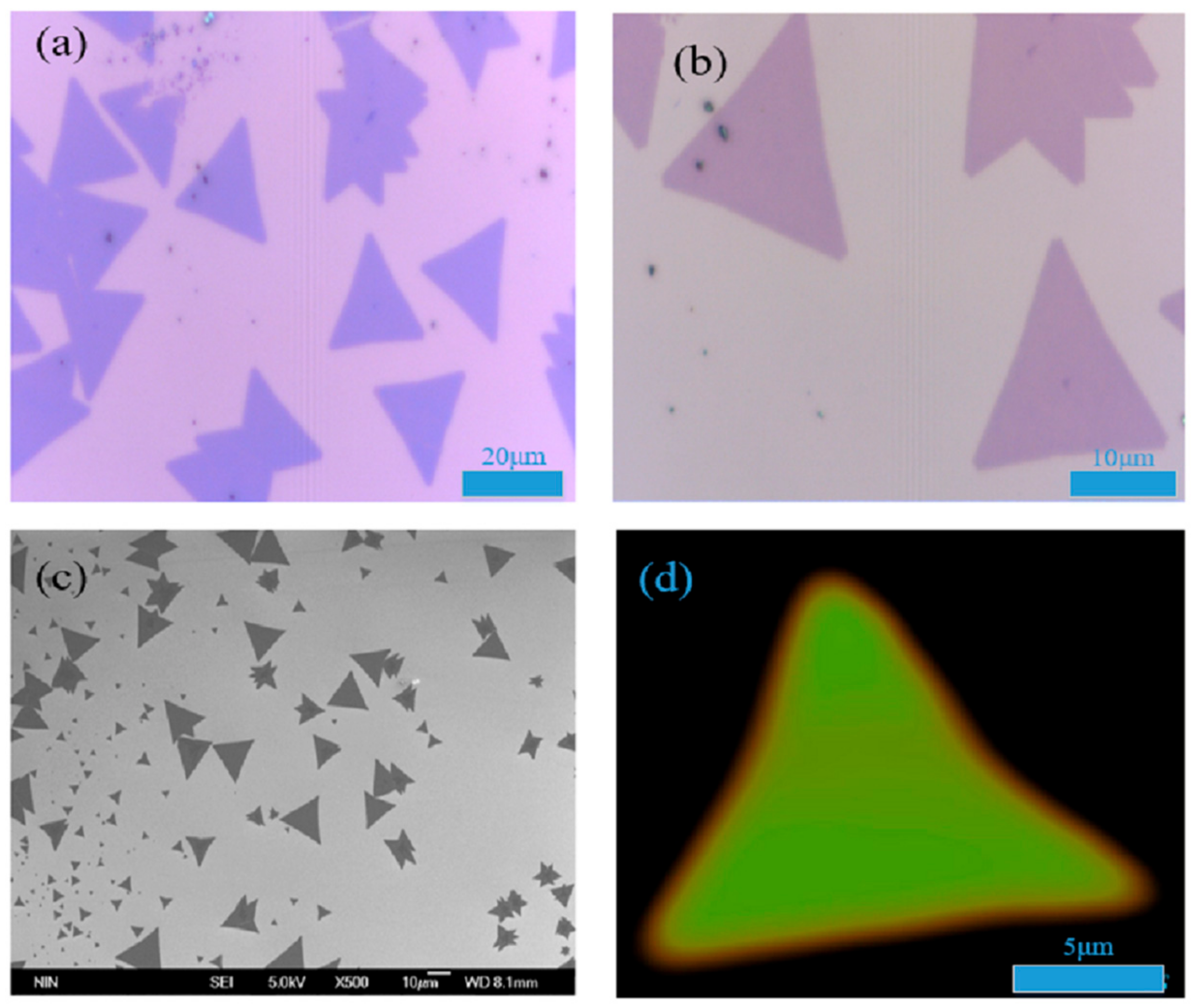
Figure 2.
(a) The Raman spectrum of monolayer MoS2 at the different test points; (b) the PL spectrum of monolayer MoS2 at the different test points; (c) the Power Raman spectrum of monolayer MoS2; and (d) the Power PL spectrum of monolayer MoS2.
Figure 2.
(a) The Raman spectrum of monolayer MoS2 at the different test points; (b) the PL spectrum of monolayer MoS2 at the different test points; (c) the Power Raman spectrum of monolayer MoS2; and (d) the Power PL spectrum of monolayer MoS2.
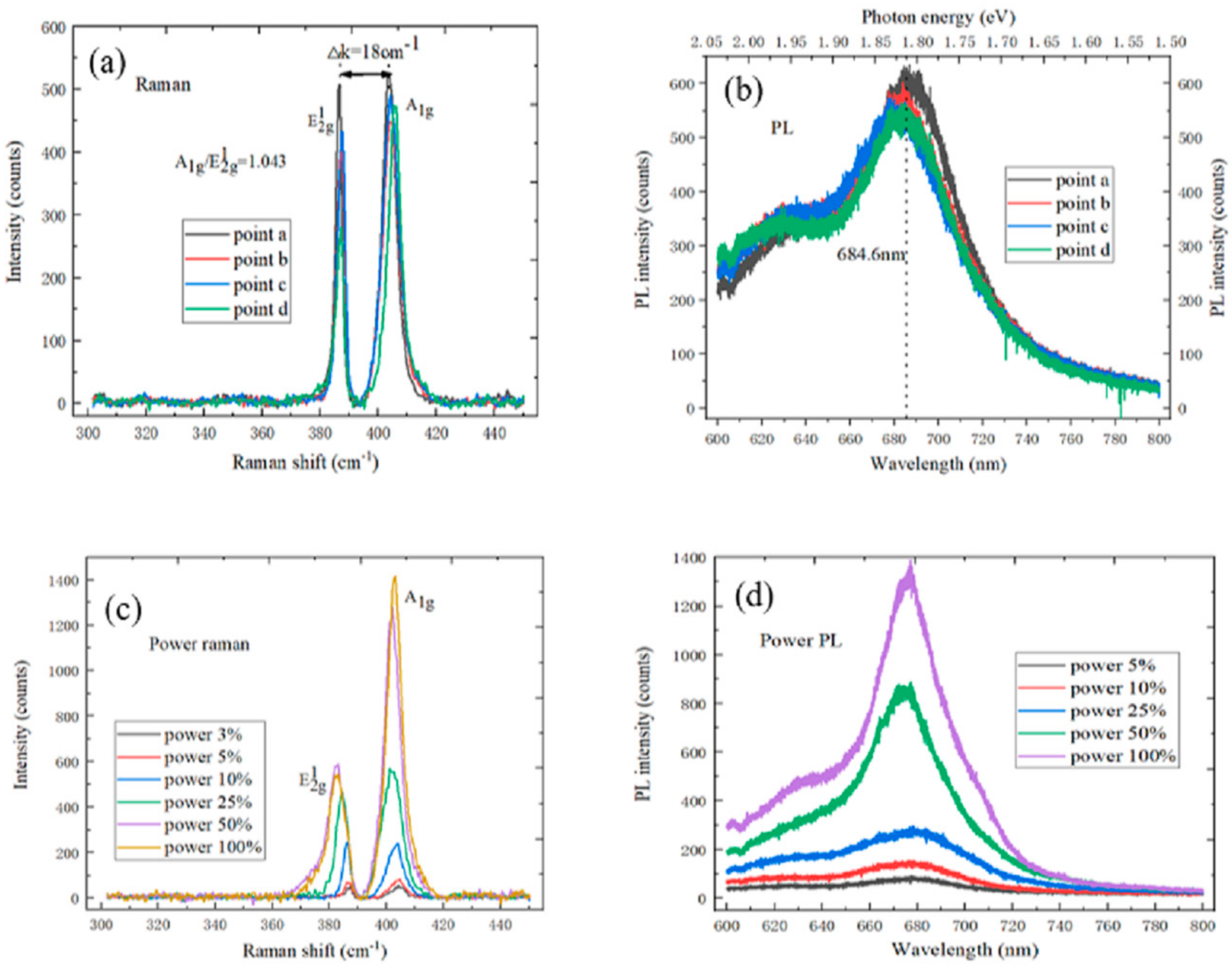
Figure 3.
The main preparation process schematic diagram of the monolayer MoS2-based field effect transistor (FET; (a)) the growth process of the high-quality triangular monolayer MoS2; (b) the photolithography and the Ar plasma etching process; (c) the electron beam evaporation process; and (d) the cleaning process of the photoresist.

Figure 4.
(a) The 10× objective optical microscope image; (b) the 50× objective optical microscope image; (c) the 100× objective optical microscope image of the monolayer MoS2-based back-gate FET; and (d) the FESEM image of the monolayer MoS2-based back-gate FET.
Figure 4.
(a) The 10× objective optical microscope image; (b) the 50× objective optical microscope image; (c) the 100× objective optical microscope image of the monolayer MoS2-based back-gate FET; and (d) the FESEM image of the monolayer MoS2-based back-gate FET.
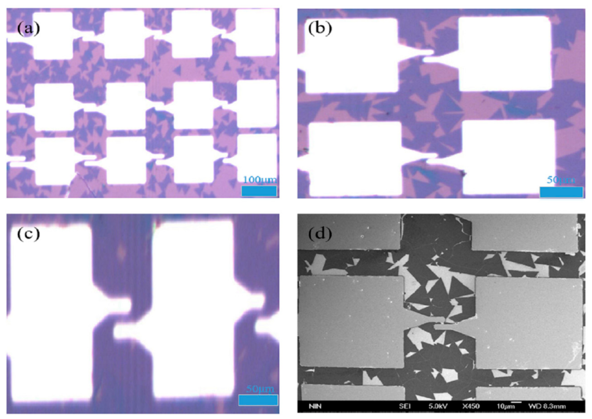
Figure 5.
The electrical test structure of the monolayer MoS2-based back-gate FET.

Figure 6.
The monolayer MoS2-based back-gate FET. (a) The Ids–Vbg transfer curve; (b) the Ids–Vbg transfer curve with the ordinate semi-logarithmic coordinate; (c) the Ids–Vds output curve; and (d) the hysteresis loop of MoS2 FET under different Vds.
Figure 6.
The monolayer MoS2-based back-gate FET. (a) The Ids–Vbg transfer curve; (b) the Ids–Vbg transfer curve with the ordinate semi-logarithmic coordinate; (c) the Ids–Vds output curve; and (d) the hysteresis loop of MoS2 FET under different Vds.
© 2019 by the authors. Licensee MDPI, Basel, Switzerland. This article is an open access article distributed under the terms and conditions of the Creative Commons Attribution (CC BY) license (http://creativecommons.org/licenses/by/4.0/).
Share and Cite
MDPI and ACS Style
Han, T.; Liu, H.; Wang, S.; Chen, S.; Xie, H.; Yang, K. Probing the Field-Effect Transistor with Monolayer MoS2 Prepared by APCVD. Nanomaterials 2019, 9, 1209. https://doi.org/10.3390/nano9091209
AMA Style
Han T, Liu H, Wang S, Chen S, Xie H, Yang K. Probing the Field-Effect Transistor with Monolayer MoS2 Prepared by APCVD. Nanomaterials. 2019; 9(9):1209. https://doi.org/10.3390/nano9091209
Chicago/Turabian StyleHan, Tao, Hongxia Liu, Shulong Wang, Shupeng Chen, Haiwu Xie, and Kun Yang. 2019. "Probing the Field-Effect Transistor with Monolayer MoS2 Prepared by APCVD" Nanomaterials 9, no. 9: 1209. https://doi.org/10.3390/nano9091209
Note that from the first issue of 2016, this journal uses article numbers instead of page numbers. See further details here.