Article

Graphene-Based THz Absorber with a Broad Band for Tuning the Absorption Rate and a Narrow Band for Tuning the Absorbing Frequency

1
College of Electronic Science and Technology, National University of Defense Technology, Changsha 410073, China
2
93046 Unit, China
*
Author to whom correspondence should be addressed.
Nanomaterials 2019, 9(8), 1138; https://doi.org/10.3390/nano9081138
Submission received: 29 June 2019 / Revised: 31 July 2019 / Accepted: 6 August 2019 / Published: 8 August 2019

Abstract

:
In this paper, we propose a broadband absorption-controllable absorber based on nested nanostructure graphene and a narrowband frequency-tunable absorber utilizing gold-graphene hybrid structure in the terahertz regime. The numerical simulation results showed that the absorption of the broadband absorber can be changed from 27% to more than 90% over 0.75 to 1.7 THz by regulating the chemical potential of graphene. With the same regulation mechanism, the absorbing peak of the narrowband absorber can be moved from 2.29 to 2.48 THz continuously with absorption of 90%. Furthermore, via the cascade of the two types of absorbers, an independently tunable dual-band absorber is constituted. Its absorption spectrum is the superposition of absorption-controllable absorber and frequency-tunable absorber. The absorptivity and operating frequency of the two absorbing bands can be tuned independently without mutual inference. Moreover, it is insensitive to the polarization and it maintains high absorption over a wide range of incident angle. For the flexibility, tunability as well as the independence of polarization and angle, this design has wide prospects in various applications.

Graphical Abstract

1. Introduction

In recent years, terahertz (THz) wave, lying between the microwaves and infrared light in the electromagnetic spectrum, has attracted great attention of researchers for its potential applications in communication, imaging, sensing, spectroscopy, etc. [1,2,3,4]. With the rapid development of THz technology, the demand for THz functional devices, such as filter, rotator, absorber, has become increasingly urgent [5,6,7]. Among these devices, THz absorber has drawn special concern due to its versatile utilization. However, the characteristics of absorber are determined once processed, thus limiting the scope of application. Traditional methods to realize tunability, such as diodes, varactors and liquid crystal, are no longer applicable in THz band [8]. Graphene, a monolayer of carbon atoms arranged in a honeycomb lattice, is an ideal candidate to design absorbers due to its remarkable mechanical properties, high carrier mobility, flexibility, and the ability to support localized surface plasmon resonance [9,10,11]. Moreover, the surface conductivity of graphene can be continuously tuned by regulating the chemical potential via electrostatic doping [12,13].
Hence, the research on development of tunable THz absorbers based on graphene has been expanding fast recently. To enhance the absorption and tunability, THz absorbers usually take advantage of patterned graphene, graphene-gold hybrid structure, and gold patches along with monolayer graphene [14,15,16,17]. However, the absorbers mentioned above generally have a single operating band or narrow absorption bandwidth. To overcome the mentioned drawbacks, different approaches have been proposed to achieve multiband or broadband function. The multiple bands can be realized either by integrating several resonators within a unit cell or stacking multiple layers of the resonators with different size separated by dielectric layers [18,19,20]. The broad bandwidth is implemented by adopting gradient structural elements, combining multilayer resonators, or nesting concentric resonators [21,22,23,24,25]. All of the mentioned absorbers can only regulate a single parameter in a specific design. Tuning both the absorption level and the frequency of different absorbing bands independently remains a challenging task for THz absorbers.
In this paper, we propose a dual-band THz graphene absorber with a broad absorption-controllable band and a narrow frequency-tunable band using the cascade method. Firstly, a broadband absorption-controllable absorber is designed. This absorber consists of periodic nanostructure graphene layer placed over dielectric layers backed on a reflector. The nested square ring and patch of graphene sheet achieves a high switching intensity of absorption over a wide band when adjusting the chemical potential via external gate voltage. Secondly, a narrowband frequency-tunable absorber is proposed. It is composed of a graphene-gold hybrid layer, a substrate spacer, and a gold grid, exhibiting a typical sandwich structure. The graphene strips deposited on the top layer dissipate the resonant power of gold structure, thus forming an absorption band. Besides, via controlling the external gate voltage, the resonant frequency can be regulated for the perturbation caused by the regulation of chemical potential in graphene strips. Finally, replacing the gold reflector of absorption-controllable absorber with the frequency-tunable absorber of the sandwiched structure, an independent tunable dual-band absorber is constructed.

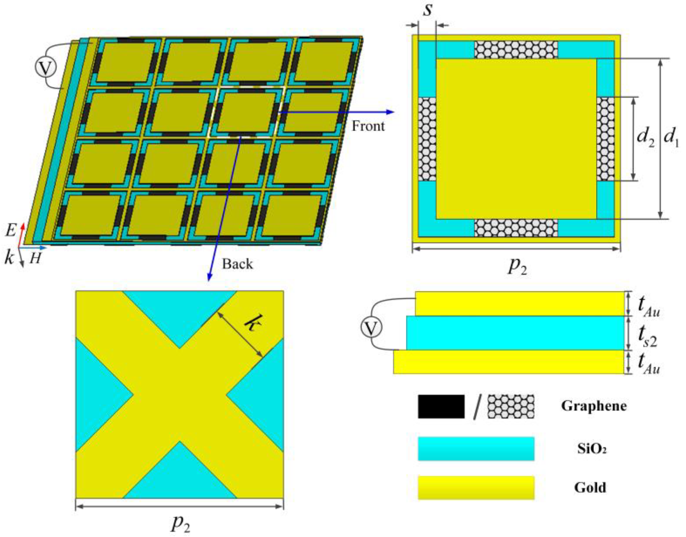
2. Materials and Methods

Graphene is considered as an infinitesimally thin material, which can be modeled as a two-dimensional sheet [26,27]. The surface conductivity of graphene is contributed by inter-band and intra-band transitions according to the Kubo formula [28,29]:
σ g = σ g i n t r a + σ g i n t e r
σ g i n t r a = 2 k B T e 2 π 2 ln [ 2 cosh ( E F 2 k B T ) ] i ω + i τ 1
σ g i n t e r = e 2 4 [ H ( ω / 2 ) + i 4 ω π 0 H ( Ω ) H ( ω / 2 ) ω 2 4 Ω 2 d Ω ]
where kB is the Boltzmann’s constant, e is the charge of an electron, and = h/2π is the reduced Planck’s constant, EF is the chemical potential (Fermi energy), τ is the relaxation time set as 0.1 ps, which is typical for experimentally studied graphene [30], T is room temperature set as 300 K, H(Ω) is defined as:
H ( Ω ) = sinh ( Ω / k B T ) cosh ( E F / k B T ) + cosh ( Ω / k B T )
According to the Pauli exclusion principle, the inter-band contribution of graphene conductivity can be safely neglected in low THz region [31]. Then, the surface impedance of a graphene monolayer is calculated by Zg = 1/σg. The real and imaginary parts of the surface impedance as a function of chemical potential is illustrated in Figure 1a,b respectively. In low THz region, the real part of the surface impedance almost remains constant, but the imaginary part grows linearly as the frequency rises. Using circuit equivalence analysis, graphene sheet behaves like the series of inductance and resistance (LR). With the increase of EF, the surface impedance decreases gradually. Therefore, the surface impedance of graphene can be effectively regulated by changing the chemical potential.
To manipulate the chemical potential of graphene via electrostatic doping, an external gate voltage is applied between the graphene layer and underneath layer. The relation between chemical potential and gate voltage can be approximately expressed by the equation [32,33]:
E F = ν F π ε 0 ε r V g / e d s
where vF is the Fermi velocity, ε0 and εr are the permittivity of free space and the substrate between electrodes, separately. Vg is the gate voltage, e is the electron charge, and ds is the thickness of the spacer between electrodes. Therefore, by regulating the surface impedance of graphene through the gate voltage, the intensity of surface plasmon resonance can be tuned effectively, thus controlling the absorption of THz absorber based on graphene.
Firstly, a broadband absorption-controllable absorber is proposed. Figure 2 gives the detailed structure of the broadband absorption-controllable absorber, which consists of a nanostructure graphene layer, a SiO2-doped Si-SiO2 sandwich structure, a gold ground. The nested square ring and patch of graphene can form resonance and excite localized surface plasmon resonances, which are hybridized with each other leading to a broadband absorption band [24]. The diagonals connect discrete units so that the electrostatic doping of periodic graphene array becomes much easier. The SiO2 layers function as spacers to separate the graphene, doped Si, and gold. It is a normal substrate and doesn’t have effects on the absorption. Doped Si plays the role of another electrode gate to realize the dynamical control of chemical potential of graphene [34,35,36]. The gold ground, whose thickness is much larger than typical skin depth in THz, reflects the incident wave like a mirror. The detailed structural parameters are listed in the caption of Figure 2. To take dispersion property of metal into consideration, the permittivity of gold is derived from Drude Model εAu = 1−ωp2/ω(ω+0), where bulk plasmon frequency of gold is ωAu = 1.37 × 10¹⁶ S−1 and the collision frequency is γ0 = 4.08 × 10¹³ S−1 [37,38]. The structural dimensions and thicknesses of different layers are shown in the caption of Figure 2.
Secondly, a narrowband frequency-tunable absorber is designed. Figure 3 depicts the schematic of the THz frequency-tunable absorber, which consists of a hybrid-SiO2-gold sandwich structure. The front layer is a square gold patch array surrounded by the gold grid, and graphene strips are evenly deposited at the bottom of the slot. The patch-grid periodic metal structure generates a parallel capacitance and inductance (LC) resonance [39,40], whose power is dissipated by the graphene strips. The SiO2 acts as a spacer and also as a support layer. The back gold grid in staggered arrangement plays the role of electrode gate. As mentioned above, graphene sheet behaves like the series of inductance and resistance. By increasing the voltage between front and back layer, the inductance of graphene drops gradually, the total paralleled inductance of the resonance decreases as well, thus moving the absorbing frequency. The detailed structural parameters are shown in the caption of Figure 3.
Finally, an independently tunable dual-band absorber is constituted by substituting the frequency-tunable absorber for the gold ground of the broadband absorption-controllable absorber. The absorption of the first operating band f1 is controlled by the voltage between nanostructure graphene and doped Si layer V1 and the frequency of the second operating band f2 is tuned via the voltage between the gold-graphene hybrid layer and back grid layer V2. Since the nanostructure graphene is almost transparent to incident wave of f2 and the frequency-tunable absorber reflects all of the transmitted wave of f1, two absorbing bands can be controlled individually without impacting each other. In theory, the doped Si can play electorate for both two different absorbers, but the distance between doped Si and gold-graphene hybrid structure is quite long, which may lead to an extremely high bias voltage. The introduction of cross feed network can solve this problem effectively. Besides, as shown in Figure 4, the periodicity of the patterned graphene layer is twice as large as that of the hybrid structure, so the unit cell of the integrated structure contains one unit of the top layer and four units of the bottom layer in the simulation.

3. Results

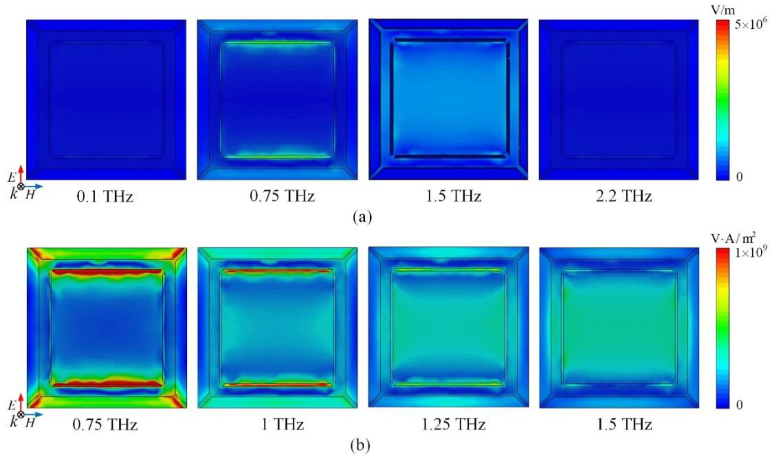
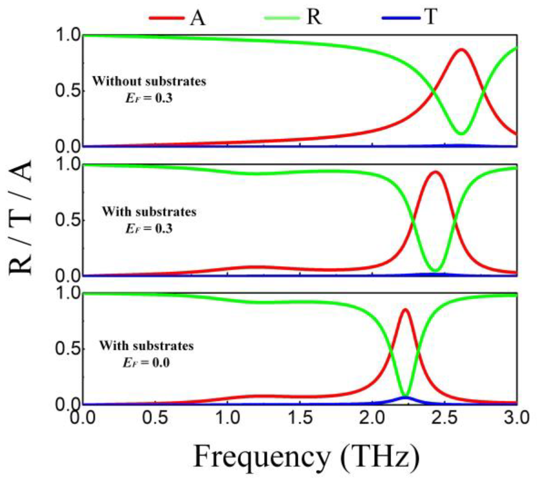
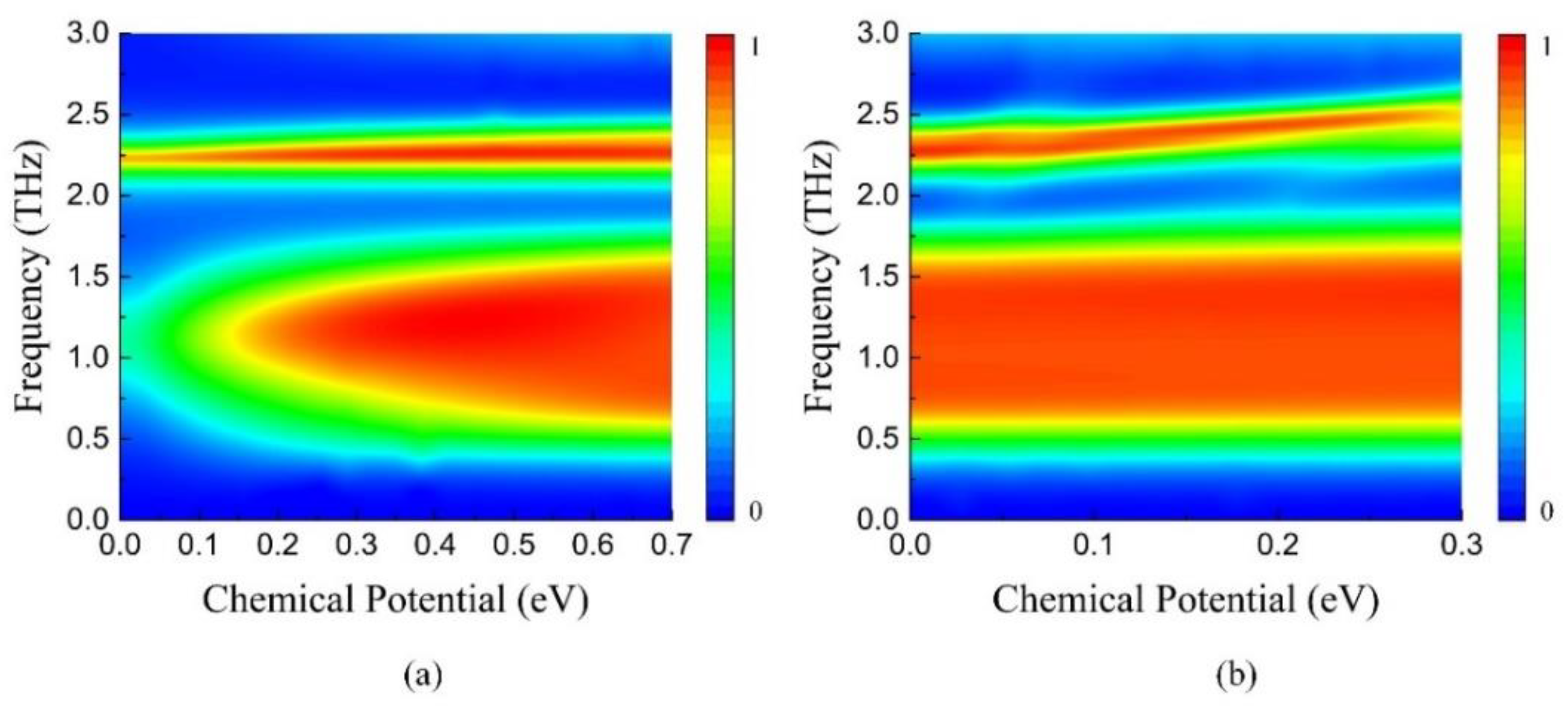
3.1. Simulations of the Broadband Absorption-Controllable Absorber

The full-wave simulation is conducted in the Computer Simulation Technology (CST) Microwave Studio (2015). It is a high-performance 3D EM analysis software package for designing, analyzing and optimizing electromagnetic (EM) components and systems [41]. The reflection and transmission are calculated using these equations: R = ǀS11ǀ2 and T = ǀS21ǀ2. Then, absorption can be obtained through A = 1−RT. The influence of the chemical potential on the absorption spectrum of the broadband absorption-controllable absorber is given in Figure 5a,b. Under normal incidence, the absorption over 90% ranges from 0.75 to 1.7 THz when EF = 0.7 eV. As EF decreases from 0.7 to 0 eV, the surface impedance of graphene drops rapidly, the absorption changes continuously from 90% to 27% corresponding the intense of resonances weakened. In the process of chemical potential decline, the rate of change in absorption is gradually accelerated, consistent with that of surface impedance shown in Figure 1.
The absorption spectrum of the broadband absorption-controllable absorber with different thick spacer thickness (ts1) is shown in the Figure 5c. With the increase of ts1, the absorption curves appear a red shift. Besides, the absorptivity drops down gradually at the upper frequency while grows slowly at the lower frequency. In ground backed absorber, the thickness of substrate between patterned graphene and ground has a negative relation with the resonant frequency. Hence, the high-frequency resonance is weakened while the high-frequency one is enhanced. As a result, the operating band of the broadband absorber shifts to lower frequency with the increase of ts1.
In order to further understand the broadband absorption mechanism, the electric field distribution and power flow of the absorber with EF = 0.7 eV are investigated. Figure 6a illustrates the electric field distribution of absorber in absorbing band (0.75 and 1.5 THz) and out of absorbing band (0.1 and 2.2 THz). Obviously, the electric field at 0.1 and 2.2 THz is rather weak corresponding to low absorption. Within the absorbing band, strong electric field is concentrated on the narrow gap and adjacent units at 0.75 THz and appears in the central square patch at 1.5 THz. It means that the resonance between the ring and the patch contributes to the low-frequency absorption while localized surface plasmon resonance caused by the square graphene patch leads to the high-frequency absorption [24]. It can be further investigated by the power flow distribution displayed in Figure 6b. Since the absorption is more than 90% in the operating band, the power flow on the top layer can show the resonant intensity and power dissipation in every position. When the frequency increases from 0.75 to 1.5 THz, the power flow is gradually weakened in the gap while greatly enhanced in the central graphene patch, which agrees well with analysis of electric field. The hybridization of resonances forms the broadband absorption. And the absorption band is decided by the dimensions of the patterned graphene layer and distance between graphene and gold ground.

3.2. Simulations of The Narrowband Frequency-Tunable Absorber

The spectrum response of the frequency-tunable absorber with EF = 0.3 eV is indicated in Figure 7. There is an absorbing point peaking at 2.7 THz. The frequency-tunable absorber is utilized to replace the gold reflector of absorption-controllable absorber when constructing the dual-band absorber. Therefore, the substrates of absorption-controllable absorber are placed on the front layer of frequency-tunable absorber to simulate together. The resonant frequency drops to 2.48 THz with absorption more than 90%. It agrees well with the conclusion of Ref. [42], that attaching substrate slab with finite length to the one side of periodic resonant structure will decrease the resonant frequency. When EF varies from 0.3 to 0 eV, the resonant position appears red shift, peaking at 2.29 THz. The parallel capacitance and inductance resonance of hybrid structure has a negative correlation between the resonant frequency and total paralleled inductance. The decrease of EF increases the inductance of graphene, which improves the total paralleled inductance of the structure thus moving the absorbing peak to lower frequency.
The distributions of electric field and surface current on the front layer and back layer are investigated to further explain the absorption mechanism. The absorption peaks at 2.48 THz when EF = 0.3 eV. As shown in Figure 8a, the electric field focuses on the gap between outer patch and outer grid on the top layer while it gathers in the oblique grid just below the position of square patch on the back layer. The absorption can be attributed to these factors: the stronger resonance between the square patch and the outer grid (on the top layer), the weaker resonance between the square patch and oblique grid (between two layers). The graphene strips in the gap mainly regulate the first factor. In other words, the capacitance of square patch along with the inductance of the outer grid, the oblique grid and the graphene forms the parallel resonance, whose power is dissipated by the graphene and gold. This principle of operation can be further verified by the current distribution displayed in Figure 8b. The current on square patch of the front layer flows from top to bottom while it is inversed on the outer grid and back layer. The anti-parallel currents are triggered by the magnetic resonance between the patches and the grids, consistent with previous research results [43].
In the narrowband frequency-tunable absorber, the absorption spectrum with different spacer thickness ts2 is indicated in Figure 8c. It can be seen that the absorptivity decreases gradually with the increase of ts2. The decrease of spacer thickness enhances the weak resonance between layers. Therefore, the intense of the top-layer resonance is weakened. As a result, the energy absorbed by graphene reduces as well, thus leading to the drop of absorption.
Furthermore, the distributions of power loss are indicated in Figure 9a. It can be seen that most of the energy is dissipated within graphene strips in accordance with the strong resonance on the front layer while a small portion of the energy is consumed in of gold-graphene should be dominant so that the performance of absorber can be tuned by the gate voltage. As shown in Figure 9b, at 2.49 THz, the energy dissipated by graphene reaches 80% and the gold also makes a small partial contribution to the loss of energy. Therefore, the frequency of absorber can be effectively regulated by the change of chemical potential of graphene.

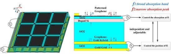
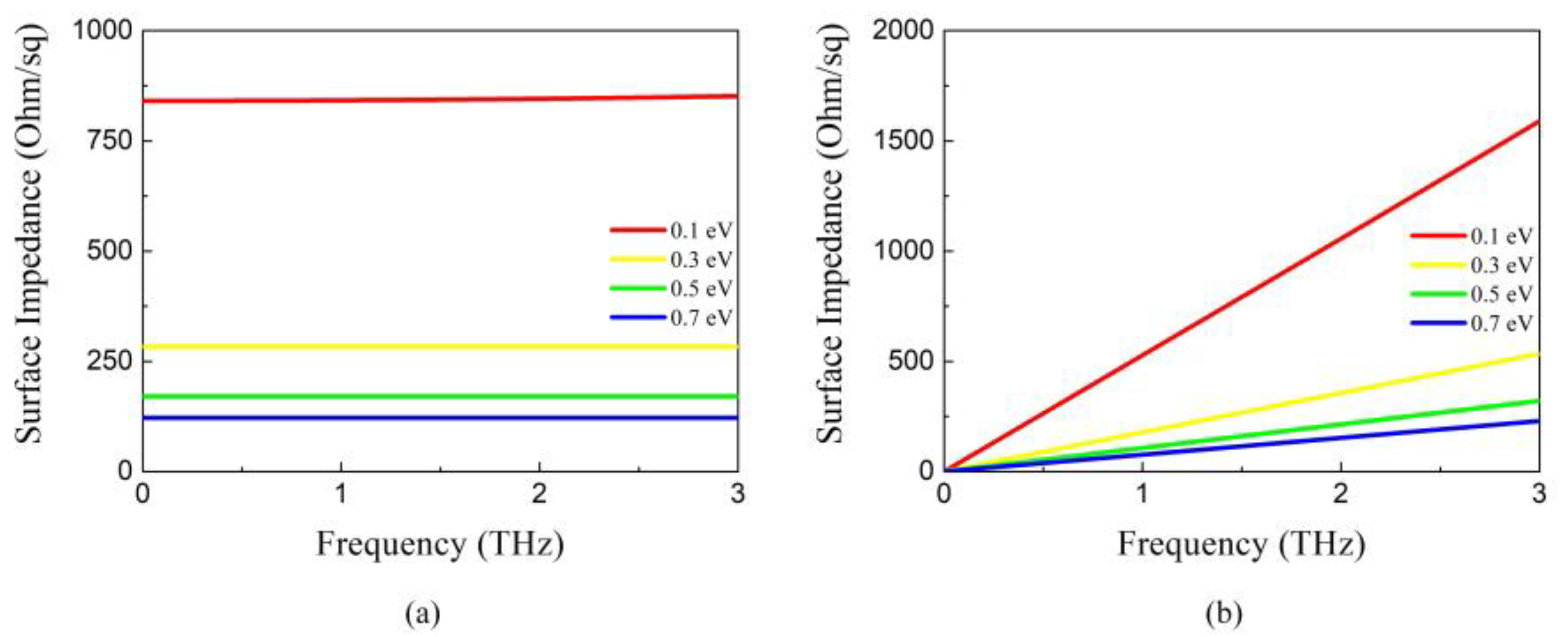
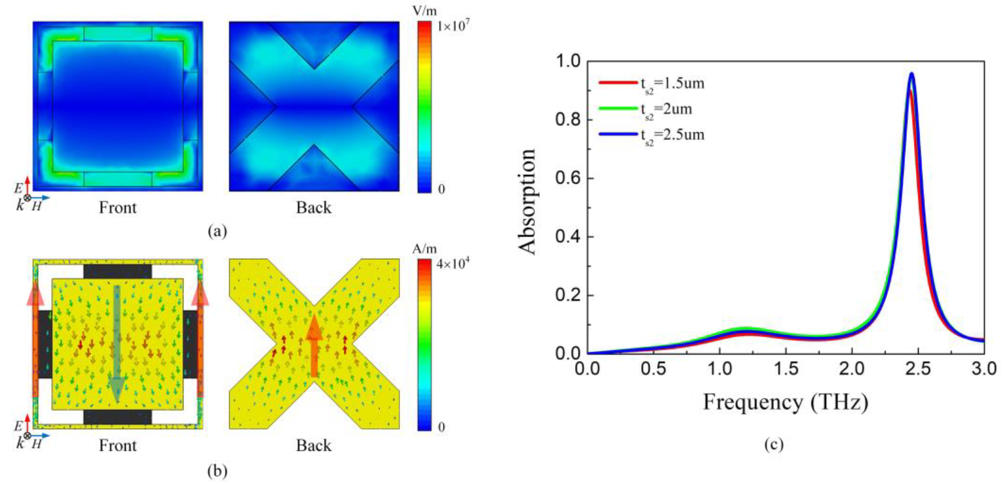
3.3. Simulations of Independently Tunable Dual-Band Absorber

Figure 10a gives the absorption spectrum of the dual-band tunable absorber as a function of the frequency and chemical potential EF1. When EF1 increases from 0 to 0.7 eV with EF2 = 0 eV, the maximum absorption of f1 (0.72 to 1.6 THz) sustains a continuous growth from 30% to more than 90%. At the same time, the second absorbing peak located at f2 = 2.3 THz maintains the absorption over 90% without frequency shift due to the fixed EF2. However, as shown in Figure 5a, the absorption of nanostructure graphene improves from 0 to 10% at 2.3 THz with the increase of EF1, which leads to the gradual expansion of effective operating bandwidth (over 90%) of the second absorbing peak. Figure 10b illustrates the relation between the absorption, frequency and EF2 with EF1 fixed at 0.7 eV. The effective absorbing band from 0.72 to 1.6 THz remains unchanged while the operating frequency of the second peak f2 moves from 2.3 to 2.5 THz, as EF2 grows from 0 to 0.3 eV. During the blue shift of f2, the effective bandwidth of the absorbing peak becomes narrow slowly, which is attributed to the decreased absorption of nanostructure graphene from 2.3 to 2.5 THz. In brief, the dual-band absorber combines the characteristics of broadband absorption-controllable absorber and narrowband frequency-tunable absorber. The absorption at f1 and the position of f2 can be tuned independently and freely.
The independence of absorption with respect to angle and polarization is essential in practical applications. Therefore, the absorption under different incident angles and polarized wave is investigated. Here, the chemical potentials EF1 and EF2 are fixed at 0.7 and 0 eV. Figure 11a depicts the absorption spectra with different polarization angle ϕ of incident wave. As ϕ varies from 0° to 90°, the absorption spectrum has no change since the C4 symmetry of the structure ensures the robustness. For TE (Transverse electric) and TM (Transverse magnetic) polarized wave under oblique incident angle θ, the absorption spectrums are shown in Figure 11b,c, respectively. The absorption at both f1 and f2 remains over 90% up to 50° for TE polarized wave. However, as θ continues to rise, there is a decline tendency for the absorption at narrow absorbing peak f2 and the low frequency portion of the broad absorbing band f1. The absorptions at these regions is triggered by the magnetic resonance on the same layer. With the increase of incident angle for TE waves, the transverse magnetic field decreases gradually, so does the intensity of magnetic resonance, resulting in a drop in absorption. As for TM polarized wave, the magnetic resonance and localized surface plasmon resonance are not affected by the incident angle so that the absorption remains more than 90% over a wide range of incidence angles up to 60°. Besides, the broad absorbing band is expanded to higher frequency when θ = 50°, because some parasitic resonances occur and become stronger at large incident angle [13,18]. The incident angle and polarization insensitivity make the proposed absorber a suitable candidate for various applications such as THz detection, sensing and telecommunication.

4. Conclusions

A dual-band tunable absorber has been designed and demonstrated theoretically, by cascading two different types of absorber. The first broad absorbing band is produced by the hybridization of different resonances in the nanostructure graphene. By changing the voltage between the graphene and doped Si to control the resonance intensity, the absorption can be continuously tuned from 30% to 90% over 0.72 to 1.6 THz. The second narrow absorbing band is formed by the magnetic resonance of gold-graphene hybrid structure. The absorbing peak with 90% absorptivity can be varied between 2.3 to 2.5 THz via controlling the voltage between hybrid layer and back grid layer. The two operating bands are controlled with different electrode gates and can be independently regulated without interference, thus greatly expanding the scope of its applications. This paper presents the general method of designing broadband absorption-controllable absorber and frequency-tunable absorber. In addition, the integration technique for combining the mentioned reconfiguration capabilities is elaborated, which is also available in other frequency for the scalability.

Author Contributions

Conceptualization, Q.Z. and C.L.; methodology, Q.Z.; software, Q.Z. and C.L.; validation, Q.Z. and C.L.; formal analysis, Q.Z. and S.Z; investigation, Q.Z. and S.Z.; resources, Q.Z.; data curation, Q.Z. and Y.Z.; writing—original draft preparation, Q.Z.; writing—review and editing, S.Z.; visualization, Q.Z.; supervision, P.L.; project administration, Q.Z.

Funding

This research is supported by the scholarship from China Scholarship Council (CSC) (201803170233).

Conflicts of Interest

The authors declare no conflict of interest.

References

  1. Kleine-ostmann, T.; Nagatsuma, T. A review on terahertz communications research. J. Infrared Millim. Terahz. Waves 2011, 32, 143–171. [Google Scholar] [CrossRef]
  2. Hu, B.B.; Nuss, M.C. Imaging with terahertz waves. Opt. Lett. 1995, 20, 1716–1718. [Google Scholar] [CrossRef] [PubMed]
  3. O’Hara, J.F.; Withayachumnankul, W.; Al-naib, I. A review on thin-film sensing with terahertz waves. J. Infrared Millim. Terahz. Waves 2012, 33, 245–291. [Google Scholar] [CrossRef]
  4. Hangyo, M.; Tani, M.; Nagashima, T. Terahertz time-domain spectroscopy of solids: A review. J. Infrared Millim. Terahz. Waves 2005, 26, 1661–1690. [Google Scholar] [CrossRef]
  5. Libon, I.H.; Baumgärtner, S.; Hempel, M.; Hecker, N.E.; Feldmann, J.; Koch, M.; Dawson, P. An optically controllable terahertz filter. Appl. Phys. Lett. 2000, 76, 2821–2823. [Google Scholar] [CrossRef]
  6. Fan, R.; Zhou, Y.; Ren, X.; Peng, R.; Jiang, S.; Xu, D.; Xiong, X.; Huang, X.; Wang, M. Freely tunable broadband polarization rotator for terahertz waves. Adv. Mater. 2015, 27, 1201–1206. [Google Scholar]
  7. Tao, H.; Bingham, C.M.; Strikwerda, A.C.; Pilon, D.; Shrekenhamer, D.; Landy, N.I.; Fan, K.; Zhang, X.; Padilla, W.J.; Averitt, R.D. Highly flexible wide angle of incidence terahertz metamaterial absorber: Design, fabrication, and characterization. Phys. Rev. B Condens. Matter Mater. Phys. 2008, 78, 2–5. [Google Scholar] [CrossRef]
  8. Zhang, Y.; Feng, Y.; Zhu, B.; Zhao, J.; Jiang, T. Graphene based tunable metamaterial absorber and polarization modulation in terahertz frequency. Opt. Express 2014, 22, 22743. [Google Scholar] [CrossRef] [PubMed]
  9. Liu, M.H.; Gorini, C.; Richter, K. Creating and steering highly directional and electron beams in graphene. Phys. Rev. Lett. 2017, 118, 066801. [Google Scholar] [CrossRef]
  10. Pasanen, P.; Voutilainen, M.; Helle, M.; Song, X.; Hakonen, P.J. Graphene for future electronics. Appl. Phys. Lett. 2016, 95, 061101. [Google Scholar] [CrossRef]
  11. Zhou, Q.; Liu, P.; Bian, L.A.; Liu, H.; Liu, C.; Chen, G. Controlling enhanced absorption in graphene metamaterial. Opt. Commun. 2018, 413, 310–316. [Google Scholar] [CrossRef]
  12. Bartolomeo, A.D.; Giubileo, F.; Santandrea, S.; Romeo, F.; Citro, R.; Schroeder, T.; Lupina, G. Charge transfer and partial pinning at the contacts as the origin of a double dip in the transfer characteristics of graphene-based field-effect transistors. Nanotechnology 2011, 22, 275702. [Google Scholar] [CrossRef] [PubMed] [Green Version]
  13. Ye, L.; Chen, Y.; Cai, G.; Liu, N.; Zhu, J.; Song, Z.; Liu, Q.H. Broadband absorber with periodically sinusoidally-patterned graphene layer in terahertz range. Opt. Express 2017, 25, 11223. [Google Scholar] [CrossRef] [PubMed]
  14. Chen, P.Y.; Farhat, M.; Bağcı, H. Graphene metascreen for designing compact infrared absorbers with enhanced bandwidth. Nanotechnology 2015, 26, 164002. [Google Scholar] [CrossRef] [PubMed]
  15. Zhao, Y.; Wu, B.; Huang, B.; Cheng, Q. Switchable broadband terahertz absorber/reflector enabled by hybrid graphene-gold metasurface. Opt. Express 2017, 25, 7161. [Google Scholar] [CrossRef] [PubMed]
  16. Jadidi, M.M.; Sushkov, A.B.; Myers-Ward, R.L.; Boyd, A.K.; Daniels, K.M.; Gaskill, D.K.; Fuhrer, M.S.; Drew, H.D.; Murphy, T.E. Tunable terahertz hybrid metal-graphene. Plasmon. Nano Lett. 2015, 15, 7099–7104. [Google Scholar] [CrossRef]
  17. Guo, X.; Hu, H.; Liao, B.; Zhu, X.; Yang, X.; Dai, Q. Perfect-absorption graphene metamaterials for surface-enhanced molecular fingerprint spectroscopy. Nanotechnology 2018, 29, 184004. [Google Scholar] [CrossRef]
  18. Yao, G.; Ling, F.; Yue, J.; Luo, C.; Ji, J.; Yao, J. Dual-band tunable perfect metamaterial absorber in the THz range. Opt. Express 2016, 24, 1518–1527. [Google Scholar] [CrossRef]
  19. Zhou, Q.; Liu, P.; Bian, L.; Cai, X.; Liu, H. Multi-band terahertz absorber exploiting graphene metamaterial. Opt. Mater. Express 2018, 8, 2928–2940. [Google Scholar] [CrossRef]
  20. Liu, B.; Tang, C.; Chen, J.; Wang, Q.; Pei, M.; Tang, H. Dual-band light absorption enhancement of monolayer graphene from surface plasmon polaritons and magnetic dipole resonances in metamaterials. Opt. Express 2017, 25, 12061–12068. [Google Scholar] [CrossRef]
  21. Amin, M.; Farhat, M.; Bağcı, H. An ultra-broadband multilayered graphene absorber. Opt. Express 2013, 21, 29938–29948. [Google Scholar] [CrossRef] [PubMed]
  22. Guo, W.; Liu, Y.; Han, T. Ultra-broadband infrared metasurface absorber. Opt. Express 2016, 24, 20586. [Google Scholar] [CrossRef] [PubMed]
  23. Yi, S.; Zhou, M.; Shi, X.; Gan, Q.; Zi, J.; Yu, Z. A multiple-resonator approach for broadband light absorption in a single layer of nanostructured graphene. Opt. Express 2015, 23, 10081. [Google Scholar] [CrossRef] [PubMed]
  24. Huang, X.; He, W.; Yang, F.; Ran, J.; Gao, B.; Zhang, W. Polarization-independent and angle-insensitive broadband absorber with a target-patterned graphene layer in the terahertz regime. Opt. Express 2018, 26, 25558–25566. [Google Scholar] [CrossRef] [PubMed]
  25. Mou, N.; Sun, S.; Dong, H.; Dong, S.; He, Q.; Zhou, L.; Zhang, L. Hybridization-induced broadband terahertz wave absorption with graphene metasurfaces. Opt. Express 2018, 26, 7181–7188. [Google Scholar] [CrossRef] [PubMed]
  26. Xiao, S.; Wang, T.; Liu, T.; Yan, X.; Li, Z.; Xu, C. Active modulation of electromagnetically induced transparency analogue in terahertz hybrid metal-graphene metamaterials. Carbon 2018, 126, 271–278. [Google Scholar] [CrossRef] [Green Version]
  27. Zhou, Q.; Zha, S.; Liu, P.; Liu, C.; Bian, L.; Zhang, J.; Liu, H.; Ding, L. Graphene based controllable broadband terahertz metamaterial absorber with transmission band. Materials 2018, 11, 2049. [Google Scholar] [CrossRef] [PubMed]
  28. Hanson, G.W. Dyadic green’s functions for an anisotropic, non-local model of biased graphene. IEEE Trans. Antenn. Propag. 2008, 56, 747–757. [Google Scholar] [CrossRef]
  29. Llatser, I.; Kremers, C.; Cabellos-Aparicio, A.; Jornet, J.M.; Alarcón, E.; Chigrin, D.N. Graphene-based nano-patch antenna for terahertz radiation. Photonics Nanostruct. Fundam. Appl. 2012, 10, 353–358. [Google Scholar] [CrossRef] [Green Version]
  30. Tymchenko, M.; Nikitin, A.Y.; Martín-Moreno, L. Faraday rotation due to excitation of magnetoplasmons in graphene. ACS Nano 2013, 7, 9780–9787. [Google Scholar] [CrossRef]
  31. Vasic, B.; Jakovljevic, M.M.; Isic, G.; Gajic, R. Tunable metamatrials based on split ring resonators and doped graphene. Appl. Phys. Lett. 2013, 103, 011102. [Google Scholar] [CrossRef]
  32. Sensale-Rodriguez, B.; Yan, R.; Rafique, S.; Zhu, M.; Li, W.; Liang, X.; Gundlach, D.; Protasenko, V.; Kelly, M.M.; Jena, D.; et al. Extraordinary control of terahertz beam reflectance in graphene electro-absorption modulators. Nano Lett. 2012, 12, 4518–4522. [Google Scholar] [CrossRef] [PubMed]
  33. Ren, L.; Zhang, Q.; Yao, J.; Sun, Z.; Kaneko, R.; Yan, Z.; Nanot, S.; Jin, Z.; Kawayama, I.; Tonouchi, M.; et al. Terahertz and infrared spectroscopy of gated large-area graphene. Nano Lett. 2012, 12, 3711–3715. [Google Scholar] [CrossRef] [PubMed]
  34. Liu, C.; Liu, P.; Yang, C.; Lin, Y.; Liu, H. Analogue of dual-controlled electromagnetically induced transparency based on graphene metamaterial. Carbon 2019, 142, 354–362. [Google Scholar] [CrossRef]
  35. He, X.; Zhong, X.; Lin, F.; Shi, W. Investigation of graphene assisted tunable terahertz metamaterials absorber. Opt. Mater. Express 2016, 6, 331–342. [Google Scholar] [CrossRef]
  36. Zhou, Q.; Zha, S.; Bian, L.A.; Zhang, J.; Ding, L.; Liu, H.; Liu, P. Independently controllable dual-band terahertz metamaterial absorber exploiting graphene. J. Phys. D Appl. Phys. 2019, 52, 255102. [Google Scholar] [CrossRef]
  37. Su, Z.; Yin, J.; Zhao, X. Terahertz dual-band metamaterial absorber based on graphene/MgF2 multilayer structures. Opt. Express 2015, 23, 1679. [Google Scholar] [CrossRef]
  38. Ordal, M.A.; Bell, R.J.; Alexander, R.W.; Long, L.L.; Querry, M.R. Optical properties of fourteen metals in the infrared and far infrared: Al, Co, Cu, Au, Fe, Pb, Mo, Ni, Pd, Pt, Ag, Ti, V, and W. Appl. Opt. 1985, 24, 4493–4499. [Google Scholar] [CrossRef]
  39. Ebrahimi, A.; Shen, Z.; Withayachumnankul, W.; Al-Sarawi, S.F.; Abbott, D. Varactor-tunable second-order bandpass frequency-selective surface with embedded bias network. IEEE Trans. Antennas Propag. 2016, 64, 1672–1680. [Google Scholar] [CrossRef]
  40. Zhou, Q.; Liu, P.; Wang, K.; Liu, H.; Yu, D. Absorptive frequency selective surface with switchable passband. AEU Int. J. Electron. Commun. 2018, 89, 160–166. [Google Scholar] [CrossRef]
  41. CST Microwave Studio by Computer Simulation Technology. Available online: http://www.cst.com (accessed on 20 June 2019).
  42. Munk, B.A. Frequency Selective Surfaces: Theory and Design; John Wiley & Sons: Hoboken, NJ, USA, 2005. [Google Scholar]
  43. Tao, H.; Landy, N.I.; Bingham, C.M.; Zhang, X.; Averitt, R.D.; Padilla, W.J. A metamaterial absorber for the terahertz regime: Design, fabrication and characterization. Opt. Express 2008, 16, 7181–7188. [Google Scholar] [CrossRef] [PubMed]
Figure 1. Surface impedance of graphene with different chemical potential (a) Real part (b) Imaginary part.
Nanomaterials 09 01138 g001
Figure 2. Schematic of the broadband absorption-controllable absorber. The values of the dimension parameters: p1 = 70, l1 = 60, l2 = 49, g = 1, w = 2, t S i O 2 = 0.3, tSi = 1, ts1 = 30, tAu = 0.5, unit: μm.
Nanomaterials 09 01138 g002
Figure 3. Schematic of the narrowband frequency-tunable absorber. The values of the dimension parameters: p2 = 35, d1 = 27, d2 = 14, s = 3, k = 11, tAu = 0.5, ts2 = 2, unit: μm.
Nanomaterials 09 01138 g003
Figure 4. Schematic of the independently tunable dual-band absorber.
Nanomaterials 09 01138 g004
Figure 5. Absorption spectrum of the broadband absorption-controllable absorber (a) EF = 0 eV and 0.7 eV (b) As a function of frequency and EF (c) with different ts1 when EF = 0.7 eV.
Nanomaterials 09 01138 g005
Figure 6. (a) The electric field distribution of the broadband absorption-controllable absorber at 0.1, 0.75, 1.5, 2.2 THz; (b) The power flow distribution of the broadband absorption-controllable absorber at 0.75, 1, 1.25, 1.5 THz.
Nanomaterials 09 01138 g006
Figure 7. Absorption, reflection and transmission of the frequency-tunable absorber.
Nanomaterials 09 01138 g007
Figure 8. (a) The electric field distribution of the narrowband frequency-tunable absorber at 2.48 THz with EF = 0.3 eV (b) The current distribution of the narrowband frequency-tunable absorber at 2.48 THz with EF = 0.3 eV (c) Absorption spectrum of the narrowband frequency-tunable absorber with different ts2 when EF = 0.3 eV.
Nanomaterials 09 01138 g008
Figure 9. (a) The power loss distribution of the narrowband frequency-tunable absorber at 2.48 THz with EF = 0.3 eV (b) The energy partition of the narrowband frequency-tunable absorber at 2.48 THz with EF = 0.3 eV.
Nanomaterials 09 01138 g009
Figure 10. Absorption spectrum of the independently tunable dual-band absorber as a function of frequency and chemical potential (a) EF1: 0–0.7 eV, EF2 = 0 eV (b) EF1 = 0.7 eV, EF2: 0–0.3 eV.
Nanomaterials 09 01138 g010
Figure 11. Absorption spectrum of the independently tunable dual-band absorber as a function of frequency and polarization angles/incident angles (a) polarization angle ϕ: 0°–90°; (b) TE, incident angle θ: 0°–60° (c) TM, incident angle θ: 0°–60°.
Nanomaterials 09 01138 g011

