Morphological and Optical Characteristics of Chitosan(1−x):Cuox (4 ≤ x ≤ 12) Based Polymer Nano-Composites: Optical Dielectric Loss as an Alternative Method for Tauc’s Model

Abstract
:
1. Introduction
2. Experimental Details
2.1. Materials and Sample Preparation
2.2. Characterization Techniques
3. Results and Discussion
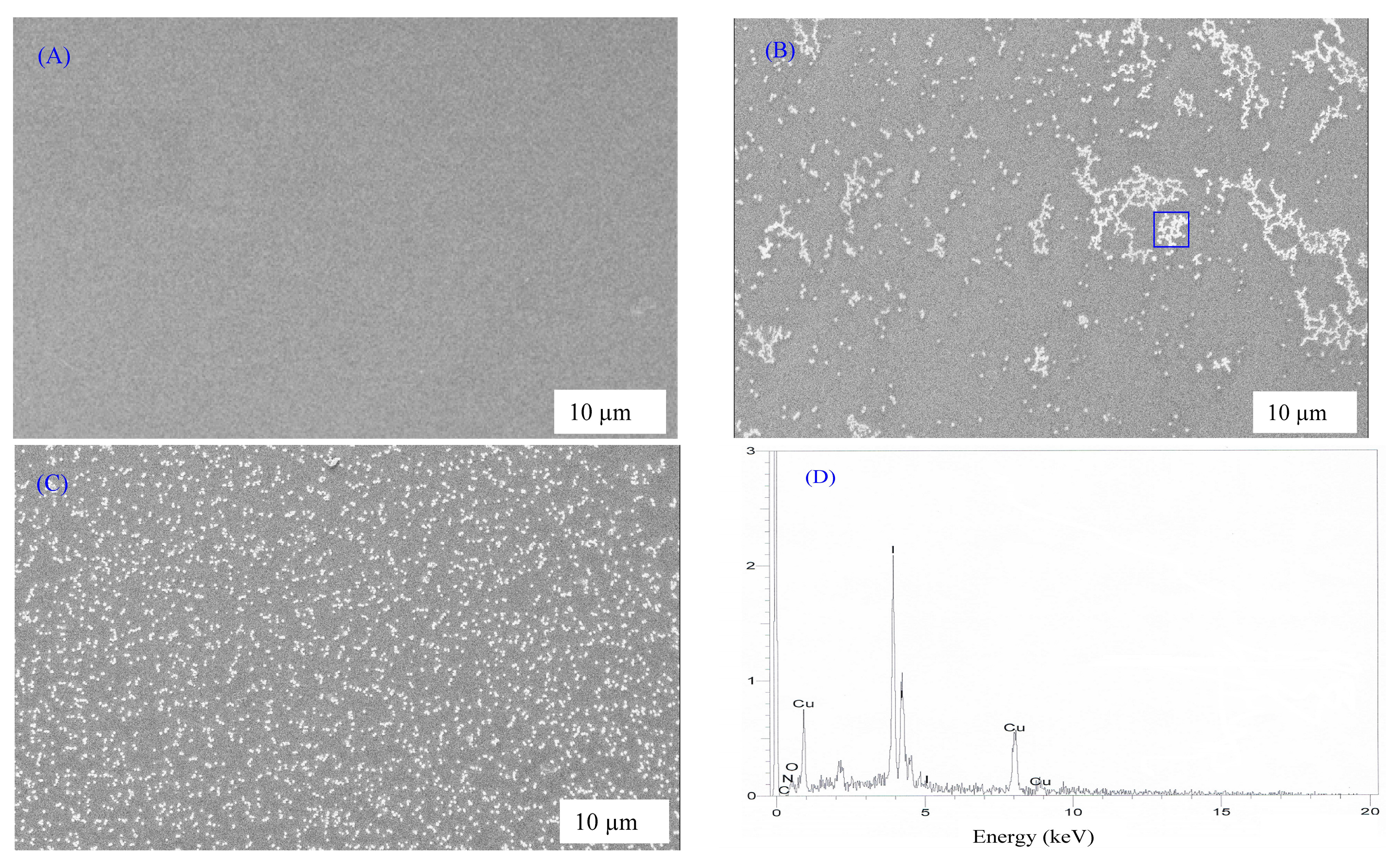
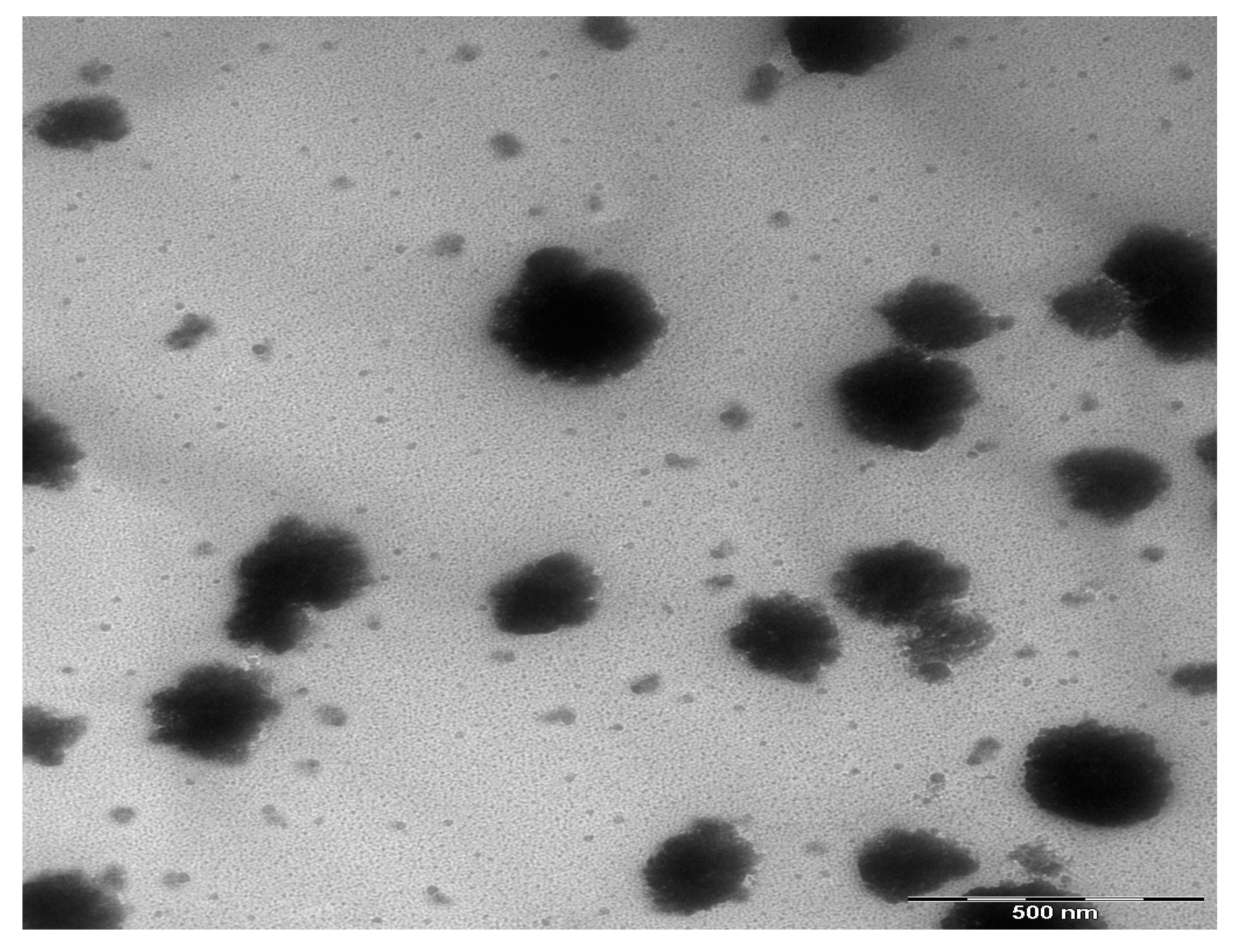
3.1. Morphological Studies
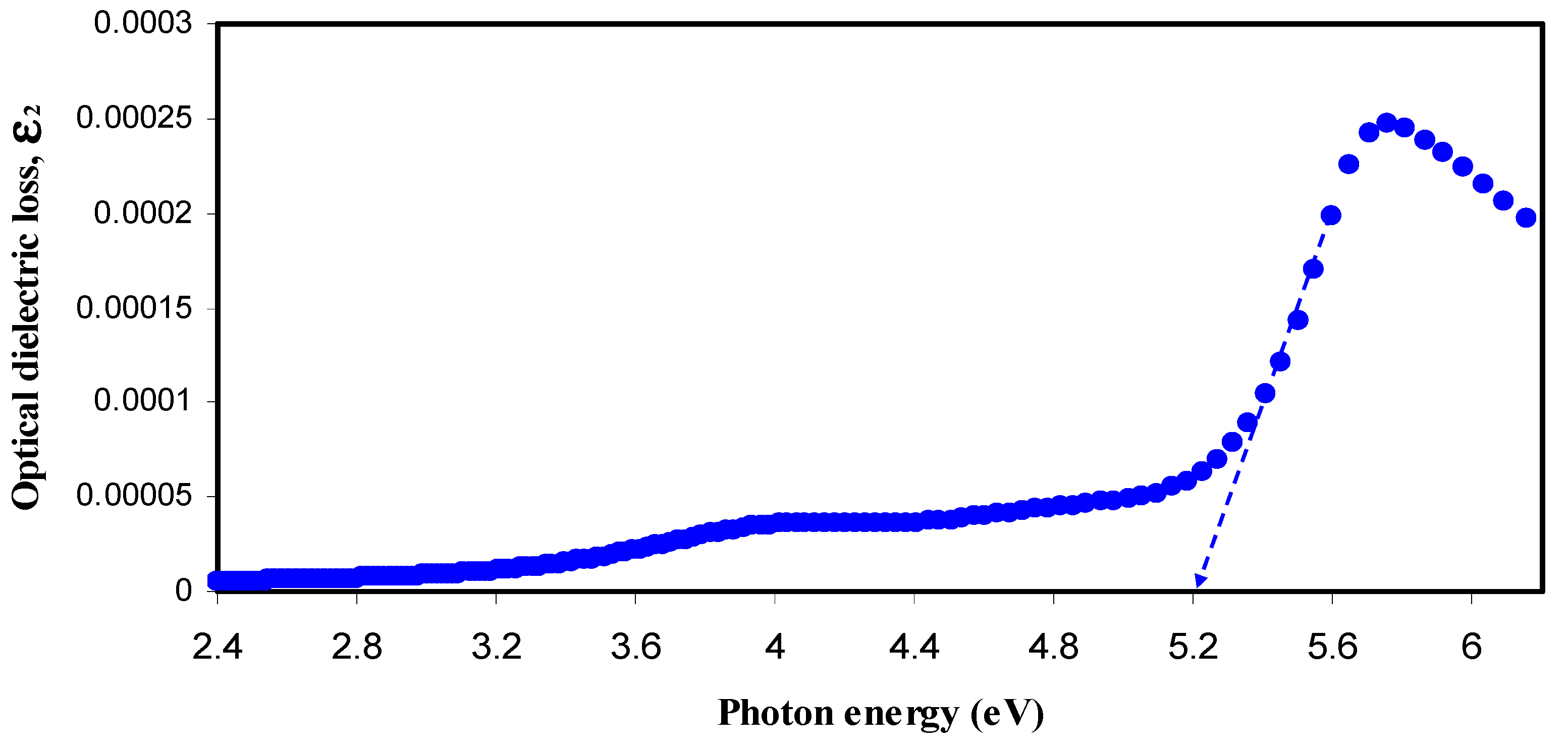
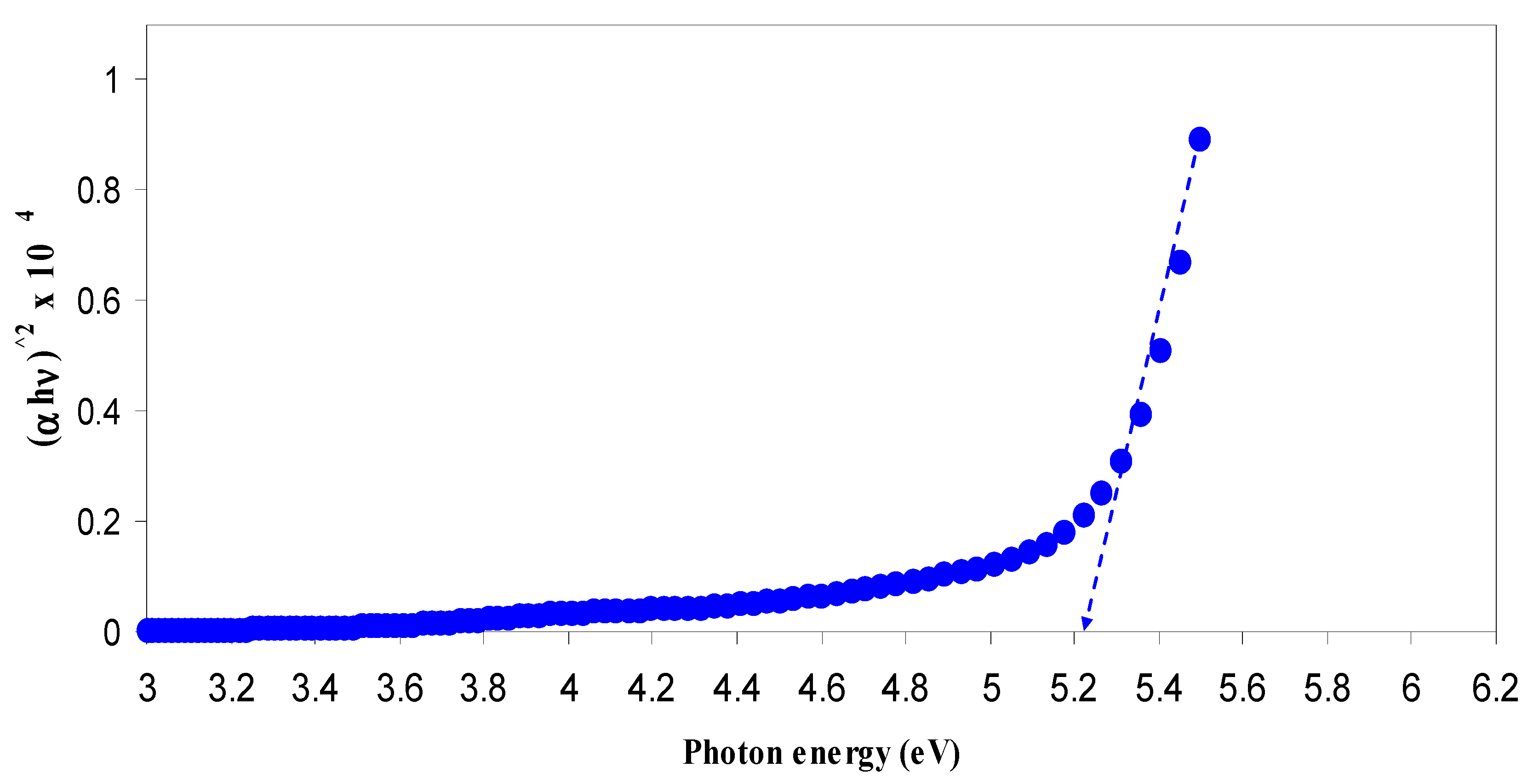
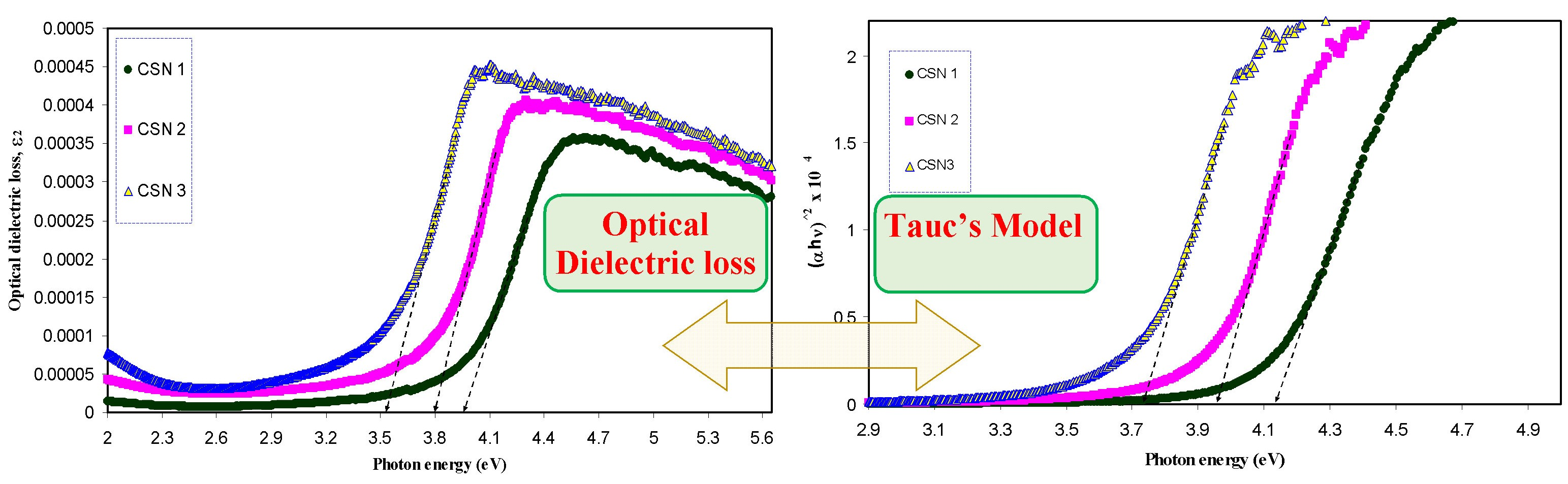
3.2. Optical Properties
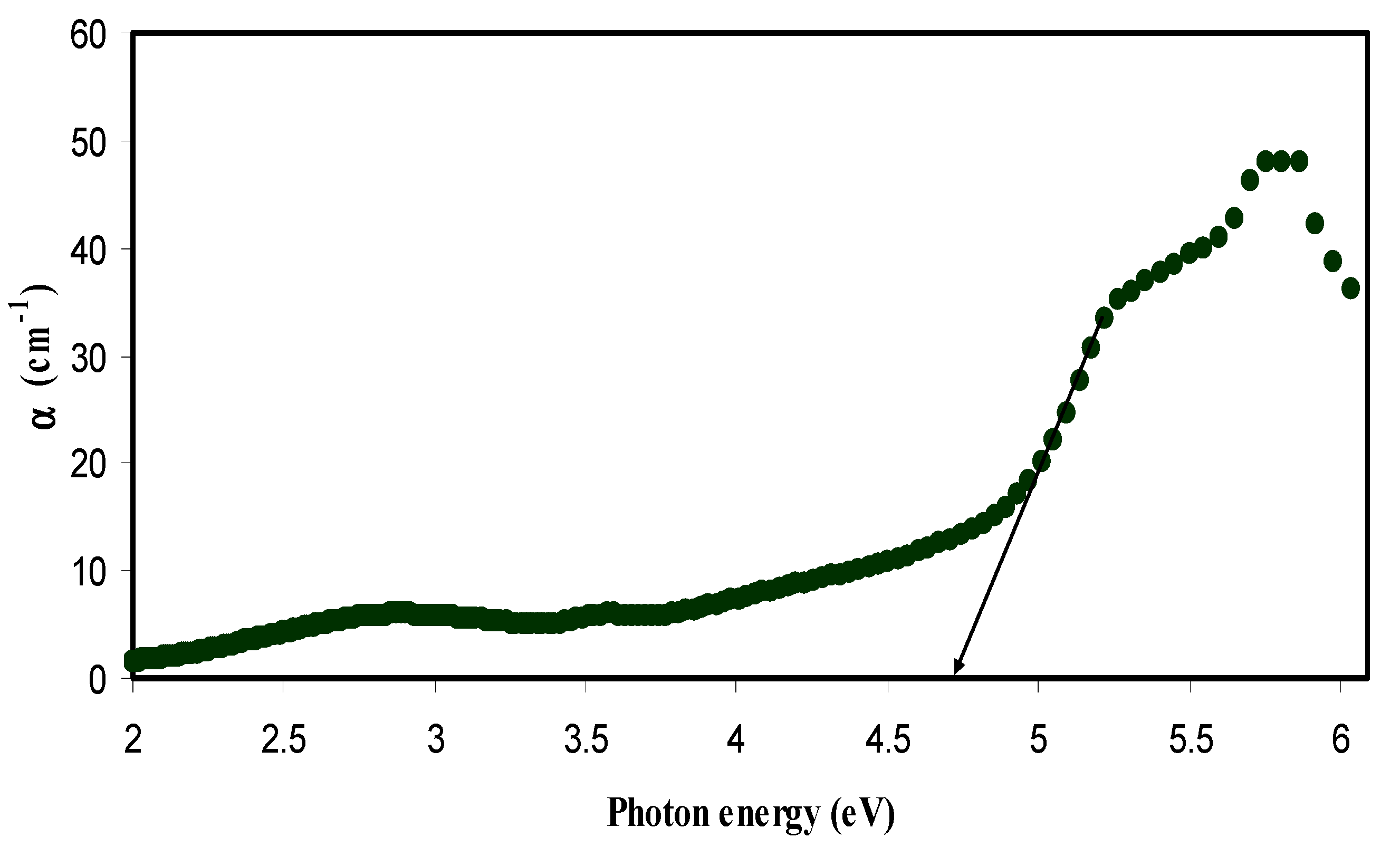
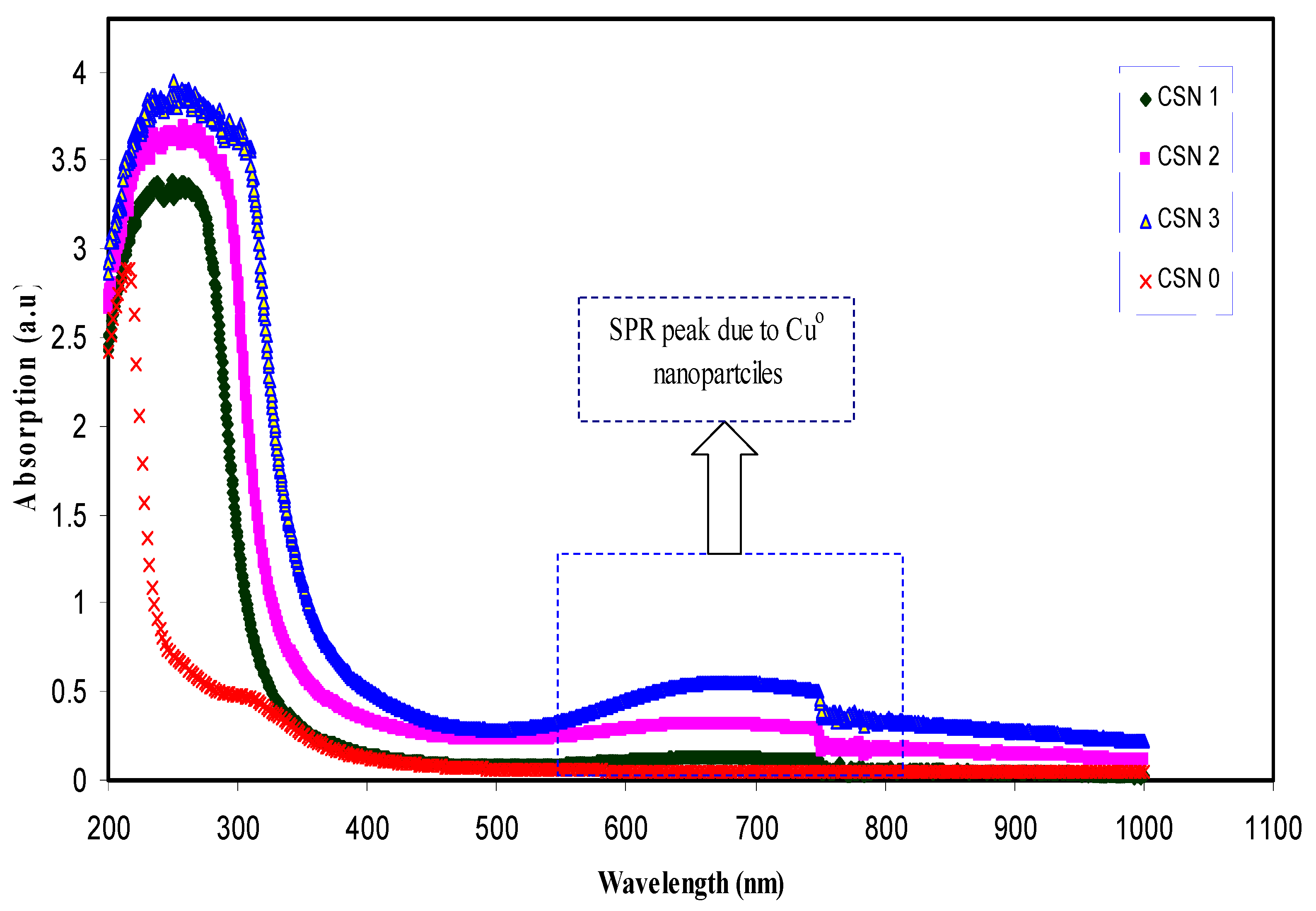
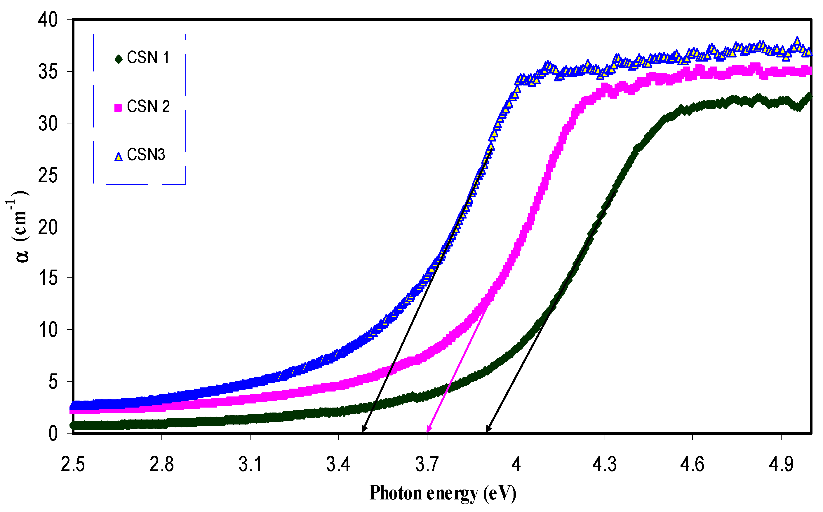
3.2.1. Absorption and Absorption Edge Study
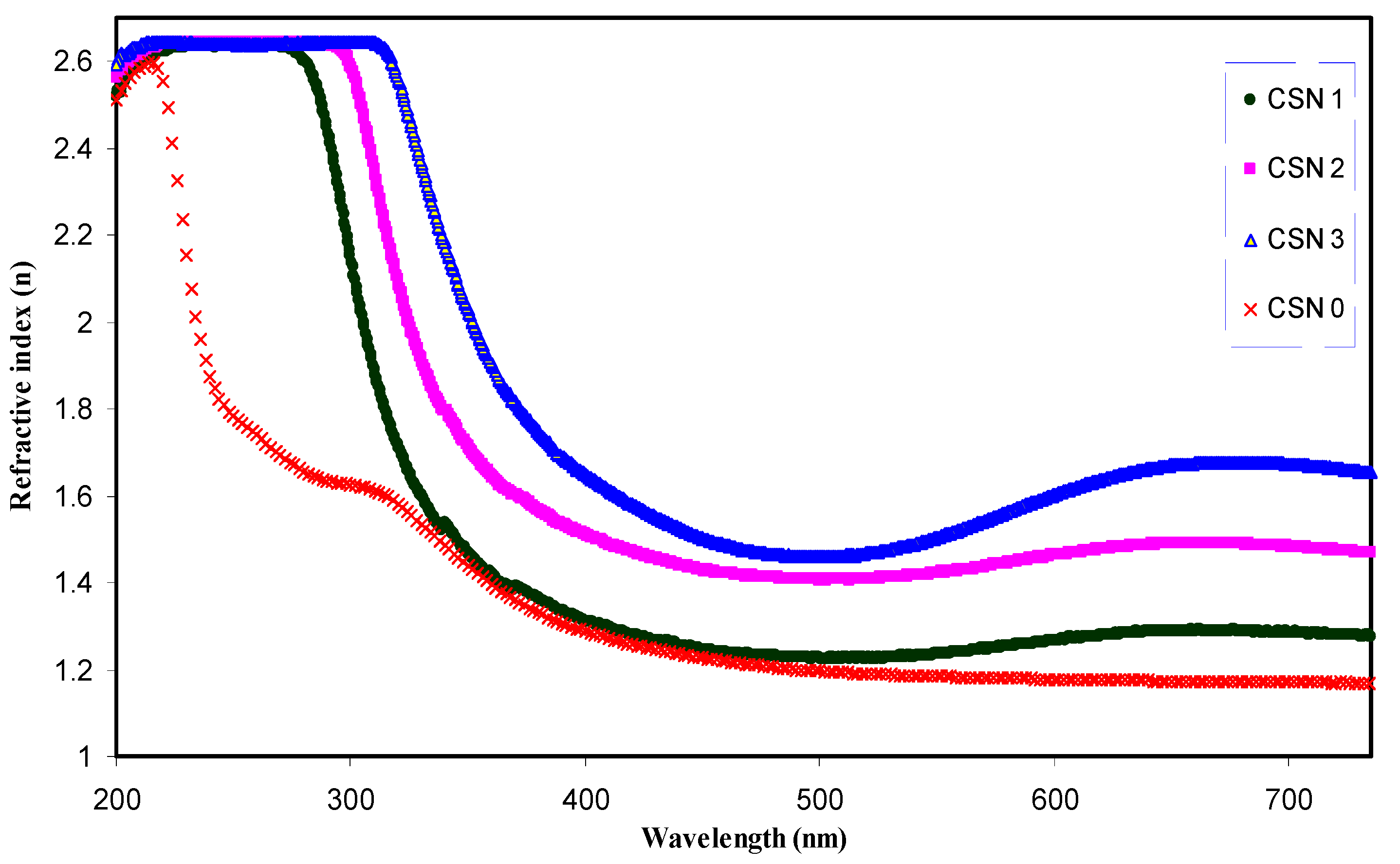
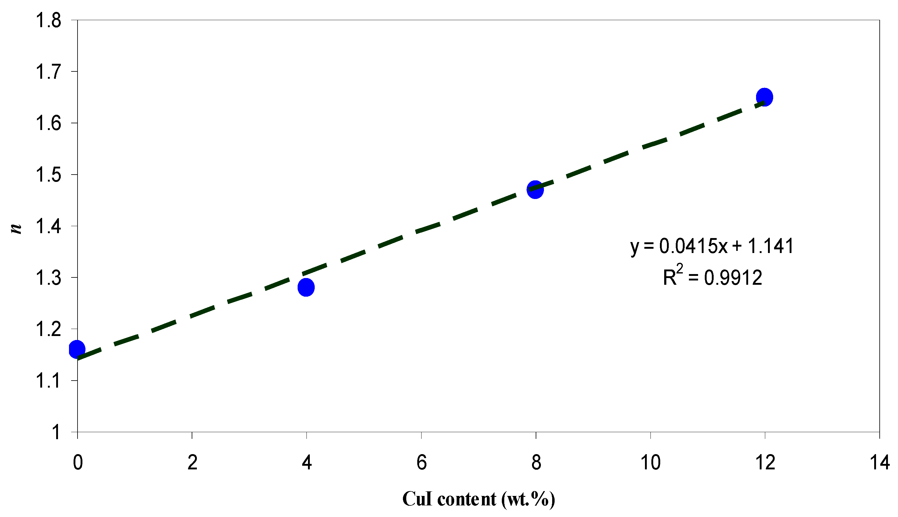
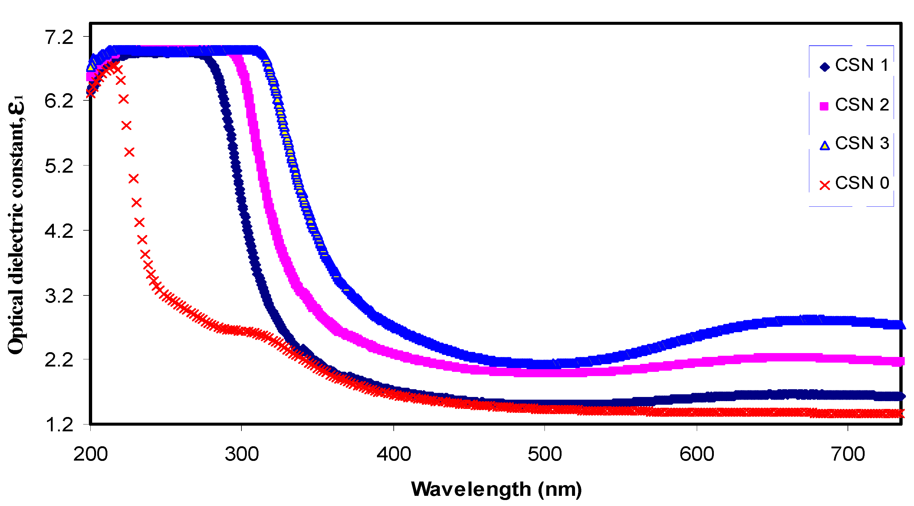
3.2.2. Refractive Index and Optical Dielectric Constant Study
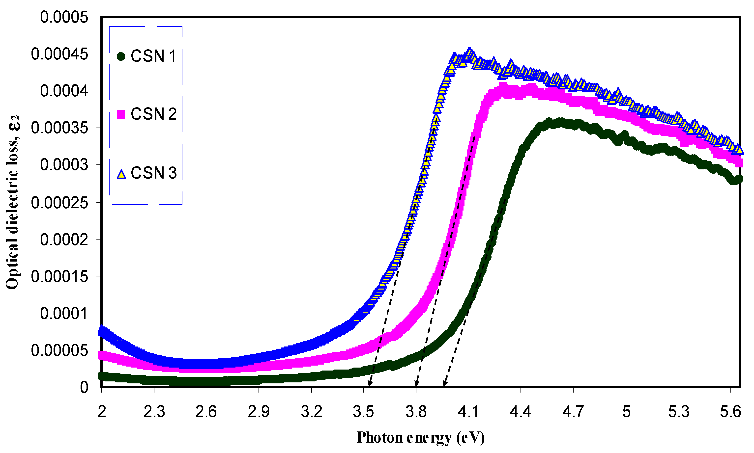
3.2.3. Band Gap Study
4. Conclusions
Acknowledgments
Conflicts of Interest
References
- Rahman, A.; Ismail, A.; Jumbianti, D.; Magdalena, S.; Sudrajat, H. Synthesis of copper oxide nano particles by using phormidium cyanobacterium. Indones. J. Chem. 2009, 9, 355–360. [Google Scholar]
- Almeida, J.M.P.; de Boni, L.; Avansi, W.; Ribeiro, C.; Longo, E.; Hernandes, A.C.; Mendonca, C.R. Generation of copper nanoparticles induced by fs-laser irradiation in borosilicate glass. Opt. Express 2012, 20, 15106. [Google Scholar] [CrossRef] [PubMed]
- Linic, S.; Aslam, U.; Boerigter, C.; Morabito, M. Photochemical transformations on plasmonic metal nanoparticles. Nat. Mater. 2015, 14, 567–576. [Google Scholar] [CrossRef] [PubMed]
- Chan, G.H.; Zhao, J.; Hicks, E.M.; Schatz, G.C.; Duyne, R.P.V. Plasmonic Properties of Copper Nanoparticles Fabricated by Nanosphere Lithography. Nano Lett. 2007, 7, 1947–1952. [Google Scholar] [CrossRef]
- Dang, T.M.D.; Le, T.T.T.; Fribourg-Blanc, E.; Dang, M.C. Synthesis and optical properties of copper nanoparticles prepared by a chemical reduction method. Adv. Nat. Sci. 2011, 2, 015009. [Google Scholar] [CrossRef]
- Pestryakov, A.N.; Petranovskii, V.P.; Kryazhov, A.; Ozhereliev, O.; Pfander, N.; Knop-Gericke, A. Study of copper nanoparticles formation on supports of different nature by UV-Vis diffuse reflectance spectroscopy. Chem. Phys. Lett. 2004, 385, 173–176. [Google Scholar] [CrossRef]
- Alzahrani, E.; Ahmed, R.A. Synthesis of Copper Nanoparticles with Various Sizes and Shapes: Application as a Superior Non-Enzymatic Sensor and Antibacterial Agent. Int. J. Electrochem. Sci. 2016, 11, 4712–4723. [Google Scholar] [CrossRef]
- Cuevas, R.; Durán, N.; Diez, M.C.; Tortella, G.R.; Rubilar, O. Extracellular Biosynthesis of Copper and Copper Oxide Nanoparticles by Stereum hirsutum, a Native White-Rot Fungus from Chilean Forests. J. Nanomater. 2015, 2015, 789089. [Google Scholar] [CrossRef]
- Zhang, D.; Gökce, B. Perspective of laser-prototyping nanoparticle-polymer composites. Appl. Surf. Sci. 2017, 392, 991–1003. [Google Scholar] [CrossRef]
- Sadananda, V.; Rajinib, N.; Rajuluc, A.V.; Satyanarayana, B. Preparation of cellulose composites with in-situ generated copper nanoparticles using leaf extract and their properties. Carbohydr. Polym. 2016, 150, 32–39. [Google Scholar] [CrossRef] [PubMed]
- Usman, M.S.; Ibrahim, N.A.; Shameli, K.; Zainuddin, N.; Yunus, W.M.Z.W. Copper Nanoparticles Mediated by Chitosan: Synthesis and Characterization via Chemical Methods. Molecules 2012, 17, 14928–14936. [Google Scholar] [CrossRef] [PubMed]
- Aziz, S.B.; Rasheed, M.A.; Abidin, Z.H.Z. Optical and Electrical Characteristics of Silver Ion Conducting Nanocomposite Solid Polymer Electrolytes Based on Chitosan. J. Electron. Mater. 2017. [Google Scholar] [CrossRef]
- Aziz, S.B.; Abidin, Z.H.Z.; Kadir, M.F.Z. Innovative method to avoid the reduction of silver ions to silver nanoparticles in silver ion conducting based polymer electrolytes. Phys. Scr. 2015, 90, 035808. [Google Scholar] [CrossRef]
- Aziz, S.B.; Abdullah, O.G.; Saber, D.R.; Rasheed, M.A.; Ahmed, H.M. Investigation of Metallic Silver Nanoparticles through UV-Vis and Optical Micrograph Techniques. Int. J. Electrochem. Sci. 2017, 12, 363–373. [Google Scholar] [CrossRef]
- Aziz, S.B.; Abdullah, O.G.; Rasheed, M.A. A novel polymer composite with a small optical band gap: New approaches for photonics and optoelectronics. J. Appl. Polym. Sci. 2017, 134, 44847. [Google Scholar] [CrossRef]
- Aziz, S.B.; Abidin, Z.H.Z.; Arof, A.K. Influence of silver ion reduction on electrical modulus parameters of solid polymer electrolyte based on chitosan-silver triflate electrolyte membrane. Express Polym. Lett. 2010, 5, 300–310. [Google Scholar] [CrossRef]
- Aziz, S.B.; Abidin, Z.H.Z. Electrical and morphological analysis of chitosan: AgTf solid electrolyte. Mater. Chem. Phys. 2014, 144, 280–286. [Google Scholar] [CrossRef]
- Wei, D.; Sun, W.; Qian, W.; Ye, Y.; Ma, X. The synthesis of chitosan-based silver nanoparticles and their antibacterial activity. Carbohydr. Res. 2009, 344, 2375–2382. [Google Scholar] [CrossRef] [PubMed]
- Vodnik, V.V.; Božanic, D.K.; Džunuzovic, E.; Vukovic, J.; Nedeljkovic, J.M. Thermal and optical properties of silver–poly(methylmethacrylate) nanocomposites prepared by in-situ radical polymerization. Eur. Polym. J. 2010, 46, 137–144. [Google Scholar] [CrossRef]
- Sanchez, C.; Belleville, P.; Popalld, M.; Nicole, L. Applications of advanced hybrid organic–inorganic nanomaterials: From laboratory to market. Chem. Soc. Rev. 2011, 40, 696–753. [Google Scholar] [CrossRef] [PubMed]
- Shea, K.J.; Loy, D.A. Bridged Polysilsesquioxanes. Molecular-Engineered Hybrid Organic-Inorganic Materials. Chem. Mater. 2001, 13, 3306–3319. [Google Scholar] [CrossRef]
- Sanchez, C.; Lebeau, B.; Chaput, F.; Boilot, J.-P. Optical Properties of Functional Hybrid Organic-Inorganic Nanocomposite. Adv. Mater. 2003, 15, 1969–1994. [Google Scholar] [CrossRef]
- Faupel, F.; Zaporojtchenko, V.; Strunskus, T.; Elbahri, M. Metal-Polymer Nanocomposites for Functional Applications. Adv. Eng. Mater. 2010, 12, 1117–1190. [Google Scholar] [CrossRef]
- Ruffino, F.; Torrisi, V.; Marletta, G.; Grimaldi, M.G. Effects of the embedding kinetics on the surface nano-morphology of nano-grained Au and Ag films on PS and PMMA layers annealed above the glass transition temperature. Appl. Phys. A 2012, 107, 669–683. [Google Scholar] [CrossRef]
- Tamaekong, N.; Liewhiran, C.; Phanichphant, S. Synthesis of Thermally Spherical CuO Nanoparticles. J. Nanomater. 2014, 2014, 507978. [Google Scholar] [CrossRef]
- Kozak, D.S.; Sergiienko, R.A.; Shibata, E.; Iizuka, A.; Nakamura, T. Non-electrolytic synthesis of copper oxide/carbon nanocomposite by surface plasma in super-dehydrated ethanol. Sci. Rep. 2016, 6, 21178. [Google Scholar] [CrossRef] [PubMed]
- Shah, M.A.; Al-Ghamdi, M.S. Preparation of Copper (Cu) and Copper Oxide (Cu2O) Nanoparticles under Supercritical Conditions. Mater. Sci. Appl. 2011, 2, 977–980. [Google Scholar]
- Aziz, S.B.; Rasheed, M.A.; Ahmed, H.M. Synthesis of Polymer Nanocomposites Based on [Methyl Cellulose](1−x):(CuS)x (0.02 M ≤ x ≤ 0.08 M) with Desired Optical Band Gaps. Polymers 2017, 9, 194. [Google Scholar] [CrossRef]
- Muniz-Miranda, M.; Gellini, C.; Simonelli, A.; Tiberi, M.; Giammanco, F.; Giorgetti, E. Characterization of Copper nanoparticles obtained by laser ablation in liquids. Appl. Phys. A 2013, 110, 829–833. [Google Scholar] [CrossRef]
- Aziz, S.B.; Abdulwahid, R.T.; Rsaul, H.A.; Ahmed, H.M. In-situ synthesis of CuS nanoparticle with a distinguishable SPR peak in NIR region. J. Mater. Sci. 2016, 27, 4163–4171. [Google Scholar] [CrossRef]
- Abdullah, O.G.; Aziz, S.B.; Omer, K.M.; Salih, Y.M. Reducing the optical band gap of polyvinyl alcohol (PVA) based nanocomposite. J. Mater. Sci. 2015, 26, 5303–5309. [Google Scholar] [CrossRef]
- Maggioni, G.; Vomiero, A.; Carturan, S.; Scian, C. Structure and optical properties of Au-polyimide nanocomposite films prepared by ion implantation. Appl. Phys. Lett. 2004, 85, 5712. [Google Scholar] [CrossRef]
- Takele, H.; Kulkarni, A.; Jebril, S.; Chakravadhanula, V.S.K.; Hanisch, C.; Strunskus, T.; Zaporojtchenko, V.; Faupel, F. Plasmonic properties of vapour-deposited polymer composites containing Ag nanoparticles and their changes upon annealing. J. Phys. D 2008, 41, 12540. [Google Scholar] [CrossRef]
- Biswas, A.; Aktas, O.C.; Schürmann, U.; Saeed, U.; Zaporojtchenko, V.; Faupel, F. Tunable multiple plasmon resonance wavelengths response from multicomponent polymer-metal nanocomposite systems. Appl. Phys. Lett. 2004, 84, 2655–2657. [Google Scholar] [CrossRef]
- Avasthi, D.K.; Mishra, Y.K.; Kabiraj, D.; Lalla, N.P.; Pivin, J.C. Synthesis of metal–polymer nanocomposite for optical applications. Nanotechnology 2007, 18, 125604. [Google Scholar] [CrossRef]
- Aziz, S.B.; Ahmed, H.M.; Hussein, A.M.; Fathulla, A.B.; Wsw, R.M.; Hussein, R.T. Tuning the absorption of ultraviolet spectra and optical parameters of aluminum doped PVA based solid polymer composites. J. Mater. Sci. 2015, 26, 8022–8028. [Google Scholar] [CrossRef]
- Deshmukh, S.H.; Burghate, D.K.; Shilaskar, S.N.; Chaudhari, G.N.; Deshmukh, P.T. Optical properties of polyaniline doped PVC-PMMA thin films. Indian J. Pure Appl. Phys. 2008, 46, 344–348. [Google Scholar]
- Bhavsar, V.; Tripathi, D. Study of refractive index dispersion and optical conductivity of PPy doped PVC films. Indian J. Pure Appl. Phys. 2016, 54, 105–110. [Google Scholar]
- Urs, T.G.; Gowtham, G.K.; Nandaprakash, M.B.; Mahadevaiah, D.; Sangappa, Y.; Somashekar, R. Determination of force constant and refractive index of a semiconducting polymer composite using UV/visible spectroscopy: A new approach. Indian J. Phys. 2017, 91, 53–56. [Google Scholar] [CrossRef]
- Potzsch, R.T.; Stahl, B.C.; Komber, H.; Voit, C.J.H.B.I. High refractive index polyvinylsulfide materials prepared by selective radical mono-addition thiol–yne chemistry. Polym. Chem. 2014, 5, 2911–2921. [Google Scholar] [CrossRef]
- Tao, P.; Li, Y.; Rungta, A.; Viswanath, A.; Gao, J.; Benicewicz, B.C.; Siegel, R.W.; Schadler, L.S. TiO2 nanocomposites with high refractive index and transparency. J. Mater. Chem. 2011, 21, 18623. [Google Scholar] [CrossRef]
- Abdulwahid, R.T.; Abdullah, O.G.; Aziz, S.B.; Hussein, S.A.; Muhammad, F.F.; Yahya, M.Y. The study of structural and optical properties of PVA: PbO2 based solid polymer nanocomposites. J. Mater. Sci. 2016, 27, 12112–12118. [Google Scholar]
- Aziz, S.B. Modifying poly (vinyl alcohol) (PVA) from insulator to small-bandgap polymer: A novel approach for organic solar cells and optoelectronic devices. J. Electron. Mater. 2016, 45, 736–745. [Google Scholar] [CrossRef]
- Biskri, Z.E.; Rached, H.; Bouchear, M.; Rached, D.; Aida, M.S. A Comparative Study of Structural Stability and Mechanical and Optical Properties of Fluorapatite (Ca5(PO4)3F) and Lithium Disilicate (Li2Si2O5) Components Forming Dental Glass–Ceramics: First Principles Study. J. Electron. Mater. 2016, 45, 5082–5095. [Google Scholar] [CrossRef]
- Ravindra, N.M.; Ganapathy, P.; Choi, J. Energy gap–refractive index relations in semiconductors—An overview. Infrared Phys. Technol. 2007, 50, 21–29. [Google Scholar] [CrossRef]
- Aziz, S.B.; Rasheed, M.A.; Hussein, A.M.; Ahmed, H.M. Fabrication of polymer blend composites based on [PVA-PVP](1−x):(Ag2S)x (0.01 ≤ x ≤ 0.03) with small optical band gaps: Structural and optical properties. Mater. Sci. Semicond. Process. 2017, 71, 197–203. [Google Scholar] [CrossRef]
- Alaya, R.; Slama, S.; Hashassi, M.; Mbarki, M.; Rebey, A.; Alaya, S. Theoretical Predictions of Structural, Electronic and Optical Properties of Dilute Bismide AlN1−xBix in Zinc-Blend Structures. J. Electron. Mater. 2017, 46, 1977–1983. [Google Scholar] [CrossRef]
- Wu, M.; Sun, D.; Tan, C.; Tian, X.; Huang, Y. Al-Doped ZnO Monolayer as a Promising Transparent Electrode Material: A First-Principles Study. Materials 2017, 10, 359. [Google Scholar] [CrossRef] [PubMed]
- Rodrguez, A.; Vergara, M.E.S.; Montalvo, V.G.; Ortiz, A.; Alvarez, J.R. Thin films of molecular materials synthesized from C32H20N10M (M = Co, Pb, Fe): Film formation, electrical and optical properties. Appl. Surf. Sci. 2010, 256, 3374–3379. [Google Scholar] [CrossRef]
- Bouzidi, C.; Horchani-Naifer, K.; Khadraoui, Z.; Elhouichet, H.; Ferid, M. Synthesis, characterization and DFT calculations of electronic and optical properties of CaMoO4. Phys. B 2016, 497, 34–38. [Google Scholar] [CrossRef]
- Feng, J.; Xiao, B.; Chen, J.C.; Zhou, C.T.; Du, Y.P.; Zhou, R. Optical properties of new photovoltaic materials: AgCuO2 and Ag2Cu2O3. Solid State Commun. 2009, 149, 1569–1573. [Google Scholar] [CrossRef]
- Logothetidis, S. Optical and electronic properties of amorphous carbon materials. Diam. Relat. Mater. 2003, 12, 141–150. [Google Scholar] [CrossRef]
- Nematollahin, M.; Yang, X.; Aas, L.M.S.; Ghadyani, Z.; Kildemo, M.; Gibson, U.J.; Reenaas, T.W. Molecular beam and pulsed laser deposition of ZnS:Cr for intermediate band solar cells. Sol. Energy Mater. Sol. Cells 2015, 141, 322–330. [Google Scholar] [CrossRef]
- Bao, H.; Ruan, X. Ab initio calculations of thermal radiative properties: The semiconductor GaAs. Int. J. Heat Mass Transf. 2010, 53, 1308–1312. [Google Scholar] [CrossRef]
- Ortenburger, I.B.; Rudge, W.E.; Herman, F. Electronic denstity of states and optical properties of polytypes of germanium and silicon. J. Non-Cryst. Solids 1972, 8–10, 653–658. [Google Scholar] [CrossRef]
- Aziz, S.B.; Abidin, Z.H.Z.; Arof, A.K. Effect of silver nanoparticles on the DC conductivity in chitosan-silver triflate polymer electrolyte. Phys. B Condens. Matter 2010, 405, 4429–4433. [Google Scholar] [CrossRef]
- Aziz, S.B.; Kadir, M.F.Z.; Abidin, Z.H.Z. Structural, morphological and electrochemical impedance study of CS: LiTf based solid polymer electrolyte: Reformulated Arrhenius equation for ion transport study. Int. J. Electrochem. Sci. 2016, 11, 9228–9244. [Google Scholar] [CrossRef]
- Aziz, S.B.; Abidin, Z.H.Z. Ion-transport study in nanocomposite solid polymer electrolytes based on chitosan: Electrical and dielectric analysis. J. Appl. Polym. Sci. 2015, 132, 41774. [Google Scholar] [CrossRef]
- Kumar, S.; Koh, J.; Tiwari, D.K.; Dutta, P.K. Optical Study of Chitosan-Ofloxacin Complex for Biomedical Applications. J. Macromol. Sci. Part A 2011, 48, 789–795. [Google Scholar] [CrossRef]
- Kumar, K.K.; Ravi, M.; Pavani, Y.; Bhavani, S.; Sharma, A.K.; Rao, V.V.R.N. Investigations on the effect of complexation of NaF salt with polymer blend (PEO/PVP) electrolytes on ionic conductivity and optical energy band gaps. Phys. B Condens. Matter 2011, 406, 1706–1712. [Google Scholar] [CrossRef]
- Al-Osaimi, J.; Al-Hosiny, N.; Abdallah, S.; Badawi, A. Characterization of optical, thermal and electrical properties of SWCNTs/PMMA nanocomposite films. Iran. Polym. J. 2014, 23, 437–443. [Google Scholar] [CrossRef]


| Sample Designation | Estimated Refractive Index from Figure 5 | Estimated Optical Dielectric Constant (ε1) from Figure 8 | Estimated Refractive Index from n = (ε1)1/2 |
|---|---|---|---|
| CSN0 | 1.16 | 1.36 | 1.16619 |
| CSN1 | 1.28 | 1.63 | 1.276715 |
| CSN2 | 1.47 | 2.17 | 1.473092 |
| CSN3 | 1.65 | 2.76 | 1.661325 |
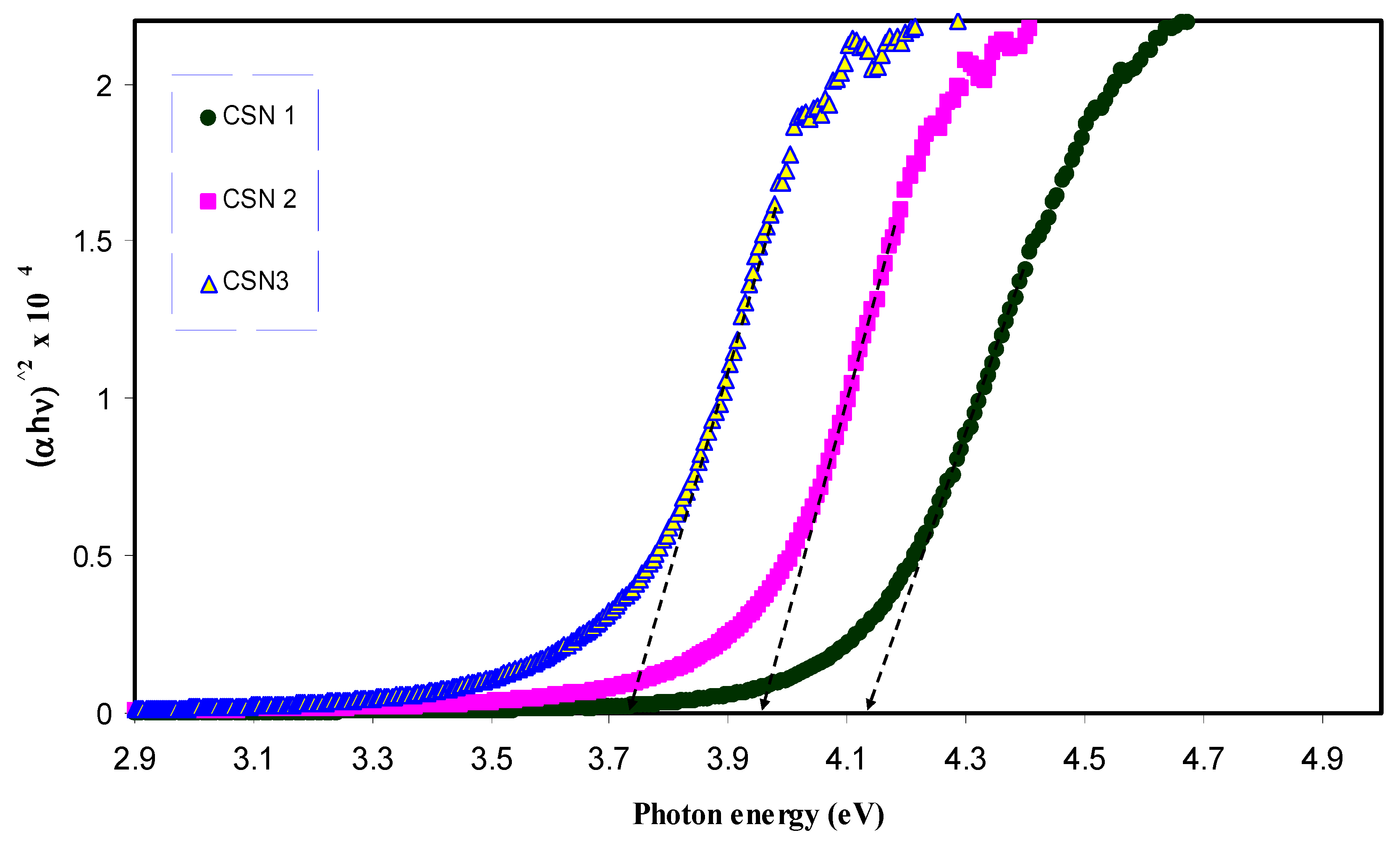
| Sample Designation | Estimated Bandgap (eV) from ε2 Plot | Eg (eV) from Tauc Method (γ = 1/2) |
|---|---|---|
| CSN0 | 5.2 | 5.24 |
| CSN1 | 3.94 | 4.14 |
| CSN2 | 3.8 | 3.95 |
| CSN3 | 3.53 | 3.72 |
© 2017 by the author. Licensee MDPI, Basel, Switzerland. This article is an open access article distributed under the terms and conditions of the Creative Commons Attribution (CC BY) license (http://creativecommons.org/licenses/by/4.0/).
Share and Cite
Aziz, S.B. Morphological and Optical Characteristics of Chitosan(1−x):Cuox (4 ≤ x ≤ 12) Based Polymer Nano-Composites: Optical Dielectric Loss as an Alternative Method for Tauc’s Model. Nanomaterials 2017, 7, 444. https://doi.org/10.3390/nano7120444
Aziz SB. Morphological and Optical Characteristics of Chitosan(1−x):Cuox (4 ≤ x ≤ 12) Based Polymer Nano-Composites: Optical Dielectric Loss as an Alternative Method for Tauc’s Model. Nanomaterials. 2017; 7(12):444. https://doi.org/10.3390/nano7120444
Chicago/Turabian StyleAziz, Shujahadeen B. 2017. "Morphological and Optical Characteristics of Chitosan(1−x):Cuox (4 ≤ x ≤ 12) Based Polymer Nano-Composites: Optical Dielectric Loss as an Alternative Method for Tauc’s Model" Nanomaterials 7, no. 12: 444. https://doi.org/10.3390/nano7120444
APA StyleAziz, S. B. (2017). Morphological and Optical Characteristics of Chitosan(1−x):Cuox (4 ≤ x ≤ 12) Based Polymer Nano-Composites: Optical Dielectric Loss as an Alternative Method for Tauc’s Model. Nanomaterials, 7(12), 444. https://doi.org/10.3390/nano7120444