
Using Si/MoS2 Core-Shell Nanopillar Arrays Enhances SERS Signal
by
 , ,
, ,
Tsung-Shine Ko
1,* ,
,
Han-Yuan Liu
1,
Jiann Shieh
2, 
De Shieh
1,
Szu-Hung Chen
3,
Yen-Lun Chen
1 and
En-Ting Lin
1 1
Department of Electronic Engineering, National Changhua University of Education, No. 2, Shi-Da Road, Changhua 50074, Taiwan
2
Department of Materials Science and Engineering, National United University, No. 2, Lianda, Miaoli 36063, Taiwan
3
Taiwan Semiconductor Research Institute, No. 26, Prosperity Road I, Hsinchu Science Park, Hsinchu 300091, Taiwan
*
Author to whom correspondence should be addressed.
Nanomaterials 2021, 11(3), 733; https://doi.org/10.3390/nano11030733
Submission received: 22 February 2021
/
Revised: 11 March 2021
/
Accepted: 13 March 2021
/
Published: 15 March 2021
(This article belongs to the Special Issue Nanomaterials and Nanostructures for Biology)
Abstract
:Two-dimensional layered material Molybdenum disulfide (MoS2) exhibits a flat surface without dangling bonds and is expected to be a suitable surface-enhanced Raman scattering (SERS) substrate for the detection of organic molecules. However, further fabrication of nanostructures for enhancement of SERS is necessary because of the low detection efficiency of MoS2. In this paper, period-distribution Si/MoS2 core/shell nanopillar (NP) arrays were fabricated for SERS. The MoS2 thin films were formed on the surface of Si NPs by sulfurizing the MoO3 thin films coated on the Si NP arrays. Scanning electron microscopy, Raman spectroscopy, and X-ray photoelectron spectroscopy were performed to characterize Si/MoS2 core-shell nanostructure. In comparison with a bare Si substrate and MoS2 thin film, the use of Si/MoS2 core-shell NP arrays as SERS substrates enhances the intensity of each SERS signal peak for Rhodamine 6G (R6G) molecules, and especially exhibits about 75-fold and 7-fold enhancements in the 1361 cm−1 peak signal, respectively. We suggest that the Si/MoS2 core-shell NP arrays with larger area could absorb more R6G molecules and provide larger interfaces between MoS2 and R6G molecules, leading to higher opportunity of charge transfer process and exciton transitions. Therefore, the Si/MoS2 core/shell NP arrays could effectively enhance SERS signal and serve as excellent SERS substrates in biomedical detection.
1. Introduction
Surface-enhanced Raman scattering (SERS) is a technique for microanalysis and biomedical detection based on the interaction between light and matter [1,2,3,4]. The two widely accepted mechanisms for the SERS effect are the electromagnetic mechanism (EM) and the chemical mechanism (CM). For the EM effect, noble metals are widely used in SERS method because of significant enhancement in signal due to high electromagnetic fields around metallic structures [5,6,7,8]. The presence of metallic structure could provide a boost of several orders of magnitude to SERS signals. On the other hand, the CM effect means the chemical interaction between the analyte molecule and the substrate [9,10,11]. In general, the SERS signal of the CM effect is extremely lower than that of the EM effect. However, using metal substrate has several disadvantages in detecting molecules. For example, the metal catalytic effect would affect the analyte molecule [12], the strong interaction between the metal and the molecule deforms the molecule structure easily [13,14], and the metal surface is prone to produce carbonization effects causing additional strong background signals generated during analysis [15]. In recent years, many studies have demonstrated that 2D materials, such as graphene, boron nitride, and molybdenum disulfide (MoS2), could be utilized as SERS substrates for biomedical detections [16,17]. Among the above materials, the MoS2 thin film has a flat surface without dangling bonds, which possesses a close proximity to the analyte molecule. Meanwhile, the feature of clean and uniform surface in MoS2 is difficult to damage the molecule [18]. Hence MoS2 has quite potential in the application of SERS.
To improve the SERS signal of MoS2 in detecting the molecule, the fabrication and development of the nanostructure of MoS2 for application of biomedical detection is worthy to investigate. Despite that many different types of MoS2 nanostructures, such as nanopatterns, nanosheets, and nanospheres, have been reported and proven to be used to enhance photocatalytic reactions by several researchers [19,20,21], little literature is available on the application of MoS2 nanostructures to the enhancement of SERS signals. Furthermore, no research has been published regarding Si/MoS2 core-shell nanostructure. Since the core-shell nanostructure could affect a larger surface with the analyte molecule during detection [22], the fabrication of a Si/MoS2 core-shell nanostructure with a high surface-to-volume ratio is expected to improve the detection signal for the applications of SERS biomedical detection.
In this work, we utilized standard semiconductor process to fabricate periodically distributed Si nanopillars (NPs) with a diameter of about 240 nm over large area. A MoO3 layer was deposited on the Si NP arrays using an evaporation system, and then the sample was placed in a high-temperature furnace for sulfurization reaction to form Si/MoS2 core-shell NP arrays. We further implemented scanning electronic microscopy (SEM), Raman spectroscopy, and X-ray photoelectron spectroscopy (XPS) to analyze material properties related to the core-shell structure. The Si/MoS2 core-shell NP array was used as a SERS substrate to detect the signal of rhodamine 6G (R6G) dye molecules. Raman results show that the SERS signal intensity of R6G molecules detected by the Si/MoS2 core-shell NP array can be increased to 75 times that of the Si substrate and 7.5 times that of the MoS2 thin film. We will further discuss and explain the possible mechanism in this article. The technique presented here may facilitate the development of MoS2 nanostructure. Meanwhile, our results could be able to provide a reference for the use of 2D material nanostructures as SERS substrates in the future.
2. Materials and Methods
2.1. Fabrication of Ordered Si NP Arrays
At first, planar p-type Si wafers with resistivity of ~10 ohm-cm were cleaned by a standard wafer clean process. Consequently, we grew thermal oxide with a thickness of ~150 nm as hard mask by using an oxidation system. The as-grown samples were coated by a positive photoresist (PR) layer, exposed to I-line stepper (Canon FPA-3000 i5+) through a mask, and then developed in regular sequence. Afterward, the CF4 plasma was applied to etching the exposed area of the SiO2 area for 120 s. After the PR layer was removed, we utilized Cl2/HBr plasma to etch Si for 250 s and the etch depth was controlled to be about 1000 nm. Eventually, the top oxide hard mask was removed by a plasma asher and buffer oxide etch progress.
2.2. Fabrication of Ordered Si/MoS2 Core-Shell NP Arrays
In order to understand the effect of using Si NP arrays for SERS, we prepared both bare Si and Si NP arrays as MoS2 substrates for comparison. We adopted the same growth procedure of MoS2 for both substrates as the following. The schematic of flowchart is shown in Figure 1. The synthesis procedures of crystal MoS2 started with MoO3 thin film coated on the Si substrates by an evaporator. Both Si and Si NP arrays substrates were pasted on the ceiling of evaporator and faced downward a tungsten boat inside the chamber. A 500 mg MoO3 tablet was placed on the tungsten boat and heated around 1000 °C for 30 s. Chamber pressure is about 5 × 10⁻⁵ torr. Then the samples were sent to a two-zone vacuum furnace for further sulfurization process to grow MoS2. The samples were fixed and inserted into a customized quartz plate with 3 mm depth grooves and faced to upstream to ensure MoO3 coated on the cylindrical sides of the Si NP arrays could fully sulfurized during the process. In the two-zone vacuum furnace heated with two different temperatures, the 8 g sulfur powders were placed at the upstream source zone while the both kinds of substrates were placed at the downstream reaction zone. We only kept the temperatures at 700 °C for 300 s in the reaction zone. The temperature in source zone reached about 500 °C when the temperature in reaction zone was 700 °C. The temperature ramping rate was set to be 5 °C /min for heating and cooling procedures. The argon with fixed flow of 200 sccm was used as the carrier gas and the pressure was around 0.1 torr. The source vapor was transported from the source zone by the carrier gas and condensed on the substrates in the reaction zone to trigger a sulfurization reaction.
2.3. Preparation of R6G Molecules
R6G dye (ACROS Organics, 99%) was dissolved in water (1 mM and 10 mM) and was dip-coated onto substrates including Si, MoS2 thin films on Si, and Si/MoS2 core-shell NP arrays. The substrates were then dried by a hot plate with setting 70 °C.
2.4. Characterizations
SEM (FEI Helios 1200+) was used for investigation of the morphology and nanostructure of the as-grown samples. The chemical configurations of the samples related to MoS2 were determined by X-ray photoelectron spectroscope (ULVAC-PHI Phi V5000), performed with an Al Kα X-ray source on the samples. The Raman spectra and SERS analyses were recorded from a confocal Raman microscopy system (Tokyo Instruments, Inc., Nanofinder 30) with a He-Ne laser excitation (laser power: 0.05 mW). The laser beam was focused in a spot of 1 μm diameter by a microscope objective with a magnification of 100 X and NA of 0.9. The acquisition time was set to 20 s for the laser measurement. The grating in spectrometer is 300 line/mm. A charge coupled device mounted in the spectrometer was cooled down about -50 °C by using a thermoelectric cooling chip to reduce noise during measurement. The spectra were calibrated by Si peak position (520 cm−1) from bulk Si substrate.
3. Results and Discussion
Figure 2a–c shows the tilt SEM images of the Si NP arrays before and after deposition of MoO3 as well as the Si/MoS2 core-shell NP arrays after sulfurization progress. From Figure 2a we observed that the diameter of a Si NP is about 240 nm. After MoO3 was deposited, the diameter of the NP is slightly increased to about 255 nm, as shown in Figure 2b. Subsequently, we found that the diameter of the NP is about 287 nm when the outer MoO3 was transformed into MoS2 and formed Si/MoS2 core-shell NP structure after sulfurization, as shown in Figure 2c. From above SEM results, we could estimate that the thickness of the MoO3 layer is about 7–8 nm, while the thickness of the MoS2 is about 23 nm formed on the lateral sides of Si NP. Note that the thickness of the MoS2 is about 3–4 times thicker from the conversion of the MoO3 layer, which is similar to the previous studies [23,24]. Moreover, we analyzed the molecule vibration modes for the planar MoS2 formed on Si and Si/MoS2 core-shell NP arrays substrates under the same MoS2 growth conditions using Raman spectroscopy. The Raman spectra and corresponding Gaussian fitting results for both planar MoS2 and Si/MoS2 core-shell NP arrays are shown in Figure 2d, which show that both samples exhibit E12g and A1g typical vibration mode peaks of MoS2, suggesting the MoO3 layer had been successfully sulfurized into MoS2. It is well known that the difference in wavenumber between the two modes would decrease with decreasing thickness of MoS2 from bulk to a few monolayers [25,26]. Since our Gaussian fitting results reveal that the difference in wavenumber between the two peaks is about 26.25 cm−1 for the planar MoS2 and 26.2 cm−1 for the Si/MoS2 core-shell NP arrays, we could further confirm that the thickness of the MoS2 thin film formed on the Si NP is bulk, which is consistent with above SEM observation.
Figure 3 shows the XPS results of the planar MoS2 and the Si/MoS2 core-shell NP arrays. The chemical composition and structural information can be further confirmed through bonding energy analysis. In Figure 3a, both XPS spectra of the planar MoS2 and the Si/MoS2 core-shell NP arrays display Mo 3d3/2, 3d5/, and S 2S located at the energy positions of 231.6, 228.5, and 225.7 eV. Figure 3b shows that S 2p1/2 and S 2p3/2 are located near the energy of 162.2 and 161.2 eV, respectively. These peak positions are in good agreement with the results of previous relevant reports, which also determine the MoS2 is in 1T stacked structure in this study [27,28,29]. On the other hand, all peaks of the planar MoS2 are slightly lower than that of Si/MoS2 core-shell NP arrays. Mahatha et al. found that the more dislocation defects and higher surface step density in MoS2 structure would reduce the relevant bonding energies of Mo and S atoms [30]. Based on this result, we infer that the use of Si NP arrays could effectively reduce defects. In addition, our XPS results did not show relevant bonding energy related to MoO3 [31], indicating that the MoO3 layer has fully reacted with sulfur vapor and transferred into MoS2 on either on the planar Si or the Si NP arrays after the sulfurization process.
We selected R6G molecules (1 mM) for the Si substrate, MoS2 thin film, and Si/MoS2 core-shell NP arrays to compare the sensitivity of SERS application. Figure 4 shows the SERS signals of the substrates obtained by Raman spectroscopy for R6G detection. It is obvious that the Raman intensity is significantly enhanced when R6G molecules are covered on the Si/MoS2 core-shell NP arrays. The intensity of all molecular vibration modes related to R6G is much higher than that of covering the MoS2 thin film and Si substrate [32]. The peak intensity of using the Si/MoS2 core-shell NP arrays is 7.5 times that of using the MoS2 thin film and 75 times that of using the Si substrate for the peak 1361 cm−1. The surface area ratio of the two substrates Si/MoS2 core-shell NP arrays and MoS2 was estimated to be about 5.22 based on the SEM observation. Therefore, the higher enhancement of the SERS signal is related to the higher surface-to-volume ratio of the Si/MoS2 core-shell NP arrays. It is worth mentioning that the Si NP array is a superhydrophilic substrate [33]. This superhydrophilic characteristic would cause the dropped R6G molecular solution to spread rapidly. In general, the larger spread R6G solution area leads to lower surface distribution density of R6G molecules. Instead, the NP arrays structure additionally provides nearly 5 times area comparing to the planar thin film, making it difficult for the R6G molecules to stack with each other. As a result, more R6G molecules could directly attach to the MoS2 thin film on Si NP and thus improve SERS signals.
In addition to R6G molecule vibration modes, the SERS result of the Si/MoS2 core-shell NP arrays also exhibit a broad band feature. Since whole measurements were carried out on almost the same period and under the same conditions, we believe that the broad band of SERS signal for the R6G on the Si/MoS2 NP arrays could not originated from relevant R6G molecule vibrations. Instead, because we used the He-Ne laser (~633 nm) as excitation source for SERS measurement, the wavenumber range 600–1800 cm−1 could be converted to the corresponding wavelength range 658–714 nm, which is very close to R6G original red-orange color. Therefore, we could suggest that the original color of R6G caused the broad band feature, which would not conflict with the idea that the Si/MoS2 core/shell NP arrays with larger area could absorb more R6G molecules. In spite of the board band feature, we still could distinguish molecule vibration modes of R6G labeled using arrow marks from the SERS signals of using the Si/MoS2 core/shell NP arrays in Figure 4. The intensities of these modes by using the Si/MoS2 core/shell NP arrays are actually stronger than that using either the planar MoS2 thin film or the Si substrate. In order to confirm the reproducibility and accuracy for the SERS result, we measured additional SERS signals from the different positions of the Si/MoS2 core/shell NP arrays, which is shown in Figure S1a–d of Supplementary Materials. We also measured an additional SERS signal of the R6G molecules (10 mM) on a Si substrate for comparison. Even though the random distribution of R6G molecules introduce the different SERS profiles, obviously the SERS results at the different positions indicate that the enhancement of the Si/MoS2 core-shell NP arrays as SERS substrates for R6G molecules is actually stronger than that of the planar MoS2 thin film and the Si substrate. Meanwhile, the results of the vibration modes are consistent with the spectrum of the R6G (10 mM) on the Si substrate. Figure S1d shows a relative low intensity in comparison to Figure S1a–c, probably due to low R6G concentration at the position where the drop point of the R6G droplet is far away.
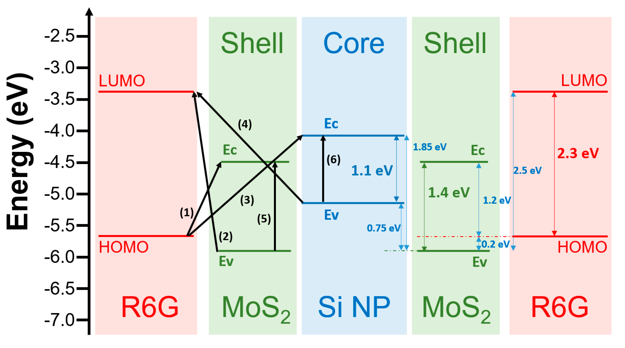
To date, many studies have demonstrated that the SERS mechanism of using 2D semiconductor material is CM and mainly due to charge transfer (CT) process happening on the interface between the molecule and the semiconductor [34,35,36,37]. There are two CT paths between molecule and semiconductor. One is that the electrons in the highest occupied molecular orbital (HOMO) of the molecules absorb enough light energy and then jump to the adjacent semiconductor conduction band to form free electrons, leaving a hole in the HOMO and forming an electron-hole pair, so called exciton. The other is that the electrons in the valence band of the semiconductor transit to the lowest unoccupied molecular orbital (LUMO) of the molecules. A schematic band diagram of the CT process between the R6G and the Si/MoS2 core-shell NP arrays is presented in Figure 5. The figure suggested that the electrons excited were transferred to a higher energy state upon absorption of light with a photon energy exceeding the energy differences via the possible transition paths (1)–(6), including (1) the HOMO of R6G to the conduction band of MoS2, (2) the valence band of MoS2 to the LUMO of R6G, (3) the HOMO of R6G to conduction band of the Si NP, (4) the valence band of Si NP to the LOMO of R6G, (5) the indirect energy gap of MoS2, and (6) the indirect energy gap of the Si NP. The corresponding energy difference is (1) 1.2 eV, (2) 2.5 eV, (3) 1.65 eV, (4) 1.75 eV, (5) 1.4 eV, and (6) 1.1 eV, respectively. Since the energy difference in path (2) is about 2.5 eV, which is larger than the photo energy 1.96 eV of the excited laser (~633 nm) we used in this study, the transition through path (2) could not happen. We believe that the opportunities of the transition path (3) and (4) are extremely low because the electrons excited via the paths have to spend much energy to pass through the thickness of MoS2 except for the R6G molecule that directly contacts the Si NP through the cracks on the surface of MoS2. Furthermore, the laser energy could penetrate either the R6G or MoS2 layers to excite electrons in the MoS2 thin film and Si NP during the SERS measurement process, leading to the path (5) and (6) related to the internal transition of indirect band gap. Therefore, the main reasons for the SERS enhancement mechanism of the Si/MoS2 core-shell NP arrays in the detection of R6G molecules may be attributed to CT process of path (1) and the exciton transitions of path (5) and (6). In comparison with the planar MoS2 thin film, we suggest that the Si/MoS2 core-shell NP arrays with higher surface-to-volume ratio could absorb more R6G molecules effectively and increase larger interface area between MoS2 and R6G. The larger interface area would further promote higher opportunity in CT and exciton resonance, leading to the enhancements R6G signals in SERS analysis. In the future, we would arrange systematically further optical experiments based on this result to understand the contribution and proportion in the SERS enhancement in terms of CT process and exciton transitions.
4. Conclusions
In conclusion, we fabricated the Si NP arrays with a diameter of about 240 nm by using the standard semiconductor process. A MoO3 layer was deposited on the Si NP arrays in an evaporation system and placed in a high-temperature furnace tube for sulfurization. Raman and XPS results confirm that the MoO3 layer around the Si NP completely transferred into MoS2 layer with a thickness of 23 nm and formed the Si/MoS2 core-shell NP arrays structure. Raman results show that using the Si/MoS2 core-shell NP arrays as a SERS substrate could enhance the R6G signals. In comparison with the planar MoS2 thin film, the superhydrophilic Si/MoS2 core-shell NP arrays with larger area could not only absorb more R6G molecules, but also cause R6G molecules difficult to stack with each other. Hence the core-shell NP arrays provide larger interface area between R6G and MoS2, leading higher opportunity of CT process and exciton transitions. The effect could enhance the SERS signals of R6G molecules. Our work indicates that the Si/MoS2 core-shell NP arrays is an excellent SERS substrate with great potential. Meanwhile, we believe this discovery will expand the application of 2D material core-shell nanostructure to the biomedical detection.
Supplementary Materials
The following are available online at https://www.mdpi.com/2079-4991/11/3/733/s1, Figure S1. SERS signals of the R6G molecules on the Si, MoS2 thin film and Si/MoS2 core-shell NP arrays substrates. An additional SERS signal of the R6G molecules (10 mM) on a Si substrate is included for comparison. The red SERS curves in (a)–(d) were measured from the different positons of the R6G molecules on the Si/MoS2 core-shell NP arrays substrates.
Author Contributions
Conceptualization and writing—original draft preparation, T.-S.K.; methodology, H.-Y.L., D.S., S.-H.C., Y.-L.C. and T.-S.K.; software, D.S., E.-T.L., H.-Y.L. and T.-S.K.; validation, T.-S.K. and D.S.; formal analysis, T.-S.K. and J.S.; investigation, T.-S.K. and J.S.; resources, J.S., S.-H.C. and T.-S.K.; data curation, T.-S.K.; writing—review and editing, J.S. and T.-S.K.; visualization, T.-S.K.; supervision, T.-S.K.; project administration, T.-S.K.; funding acquisition, T.-S.K. All authors have read and agreed to the published version of the manuscript.
Funding
This research was funded by Ministry of Science and Technology of Taiwan, grant numbers MOST 108-2221-E-018-007, MOST 109-2221-E-018-012, and MOST 110-2731-M-005-001 (ESCA00003100).
Institutional Review Board Statement
Not applicable.
Informed Consent Statement
Not applicable.
Data Availability Statement
Data is contained within the article or Supplementary Material.
Acknowledgments
The authors are also grateful to Taiwan Semiconductor Research of Institute for the semiconductor process support. The authors also thank J.-Y. Chen for the assistance on the Raman instrument and useful discussions.
Conflicts of Interest
The authors declare no conflict of interest.
References
- Wu, D.-Y.; Liu, X.-M.; Duan, S.; Xu, X.; Ren, B.; Lin, S.-H.; Tian, Z.-Q. Chemical Enhancement Effects in SERS Spectra: A Quantum Chemical Study of Pyridine Interacting with Copper, Silver, Gold and Platinum Metals. J. Phys. Chem. C 2008, 112, 4195–4204. [Google Scholar] [CrossRef]
- Yamada, H.; Nagata, H.; Toba, K.; Nakao, Y. Charge-transfer band and sers mechanism for the pyridine-Ag system. Surf. Sci. 1987, 182, 269–286. [Google Scholar] [CrossRef]
- Mosier-Boss, P.A. Review of SERS Substrates for Chemical Sensing. Nanomaterials 2017, 7, 142. [Google Scholar] [CrossRef] [PubMed] [Green Version]
- Schatz, G.C.; Young, M.A.; Duyne, R.P.V. Topics in Applied Physics. In Surface-Enhanced in Applied Physics; Kneipp, K., Moskovits, M., Kneipp, H., Eds.; Springer: Berlin/Heidelberg, Germany, 2006; Volume 19. [Google Scholar]
- Freeman, R.G.; Grabar, K.C.; Allison, K.J.; Bright, R.M.; Davis, J.A.; Guthrie, A.P.; Hommer, M.B.; Jackson, M.A.; Smith, P.C.; Walter, D.G.; et al. Self-Assembled Metal Colloid Monolayers: An Approach to SERS Substrates. Science 1995, 267, 1629–1632. [Google Scholar] [CrossRef] [PubMed]
- Singh, J.P.; Chu, H.Y.; Abell, J.; Tripp, R.A.; Zhao, Y. Flexible and mechanical strain resistant large area SERS active substrates. Nanoscale 2012, 4, 3410–3414. [Google Scholar] [CrossRef]
- Abdelsalam, M.E.; Bartlett, P.N.; Baumberg, J.J.; Cintra, S.; Kelf, T.A.; Russell, A.E. Electrochemical SERS at a structured gold surface. Electrochem. Commun. 2005, 7, 740–744. [Google Scholar] [CrossRef] [Green Version]
- Dridi, H.; Haji, L.; Moadhen, A. Studies of SERS efficiency of gold coated porous silicon formed on rough silicon backside. Appl. Surf. Sci. 2017, 426, 1190–1197. [Google Scholar] [CrossRef]
- Xia, L.; Chen, M.; Zhao, X.; Zhang, Z.; Xia, J.; Xu, H.; Sun, M. Visualized method of chemical enhancement mechanism on SERS and TERS. J. Raman Spectrosc. 2014, 45, 533–540. [Google Scholar] [CrossRef]
- Chen, R.; Jensen, L. Interpreting the chemical mechanism in SERS using a Raman bond model. J. Chem. Phys. 2020, 152, 024126. [Google Scholar] [CrossRef] [Green Version]
- Sharma, B.; Frontiera, R.R.; Henry, A.-I.; Ringe, E.; Duyne, R.P.V. SERS: Materials, applications, and the future. Mater. Today 2012, 15, 16–25. [Google Scholar] [CrossRef]
- Hvolbæk, B.; Janssens, T.V.W.; Clausen, B.S.; Falsig, H.; Christensen, C.H.; Nørskov, J.K. Catalytic Activity of Au nanoparticles. Nano Today 2007, 2, 14–18. [Google Scholar] [CrossRef]
- Guerrini, L.; Jurasekova, Z.; Domingo, C.; Pérez-Méndez, M.; Leyton, P.; Campos-Vallette, M.; Garcia-Ramos, J.V.; Sanchez-Cortes, S. Importance of Metal–Adsorbate Interactions for the Surface-enhanced Raman Scattering of Molecules Adsorbed on Plasmonic Nanoparticles. Plasmonic 2007, 2, 147–156. [Google Scholar] [CrossRef]
- Dery, S.; Berg, I.; Kim, S.; Cossaro, A.; Verdini, A.; Floreano, L.; Toste, F.D.; Gross, E. Strong Metal–Adsorbate Interactions Increase the Reactivity and Decrease the Orientational Order of OH-Functionalized N-Heterocyclic Carbene Monolayers. Langmuir 2020, 36, 697–703. [Google Scholar] [CrossRef] [PubMed]
- Xu, W.; Ling, X.; Xiao, J.; Dresselhaus, M.S.; Kong, J.; Xu, H.; Liu, Z.; Zhang, J. Surface enhanced Raman spectroscopy on a flat graphene surface. Proc. Natl. Acad. Sci. USA 2012, 109, 9281–9286. [Google Scholar] [CrossRef] [PubMed] [Green Version]
- Qiu, H.; Li, Z.; Gao, S.; Chen, P.; Zhang, C.; Jiang, S.; Li, H. Large-area MoS2 thin layers directly synthesized on Pyramid-Si substrate for surface-enhanced Raman scattering. RSC Adv. 2015, 5, 83899–83905. [Google Scholar] [CrossRef]
- Dai, Z.; Xiao, X.; Wu, W.; Zhang, Y.; Liao, L.; Guo, S.; Jiang, C. Plasmon-driven reaction controlled by the number of graphene layers and localized surface plasmon distribution during optical excitation. Light-Sci. Appl. 2015, 4, e342–e348. [Google Scholar] [CrossRef]
- Ling, X.; Fang, W.J.; Lee, Y.H.; Araujo, P.T.; Zhang, X.; Rodriguez-Nieva, J.F.; Lin, Y.X.; Zhang, J.; Kong, J.; Dresselhaus, M.S. Raman Enhancement Effect on Two-Dimensional Layered Materials: Graphene, h-BN and MoS2. Nano Lett. 2014, 14, 3033–3040. [Google Scholar] [CrossRef]
- Zhang, X.; Suo, H.; Zhang, R.; Niu, S.; Zhao, X.Q.; Zheng, J.; Guo, C. Photocatalytic activity of 3D flower-like MoS2 hemispheres. Mater. Res. Bull. 2018, 100, 249–253. [Google Scholar] [CrossRef]
- Vattikuti, S.V.P.; Byon, C.; Reddy, C.V.; Ravikumar, R.V.S.S.N. Improved photocatalytic activity of MoS2 nanosheets decorated with SnO2 nanoparticles. RSC Adv. 2015, 5, 86675–86684. [Google Scholar] [CrossRef]
- Liu, Y.; Hu, K.; Hu, E.; Guo, J.; Han, C.; Hu, X. Double hollow MoS2 nano-spheres: Synthesis, tribological properties, and functional conversion from lubrication to photocatalysis. Appl. Surf. Sci. 2017, 392, 1144–1152. [Google Scholar] [CrossRef]
- Gu, L.; Zheng, K.; Zhou, Y.; Li, J.; Mo, X.; Patzke, G.R.; Chen, G. Humidity sensors based on ZnO/TiO2 core/shell nanorod arrays with enhanced sensitivity. Sens. Actuators B Chem. 2011, 159, 1–7. [Google Scholar] [CrossRef] [Green Version]
- Heyne, M.H.; Chiappe, D.; Meersschaut, J.; Nuytten, T.; Conard, T.; Bender, H.; Huyghebaert, C.; Radu, I.P.; Caymax, M.; Marneffe, J.-F.D.; et al. Multilayer MoS2 growth by metal and metal oxide sulfurization. J. Mater. Chem. C 2016, 4, 1295–1304. [Google Scholar] [CrossRef] [Green Version]
- Kumar, P.; Singh, M.; Sharma, R.K.; Reddy, G.B. Sulfurization of α-MoO3 nanostructured thin film. AIP Conf. Proc. 2015, 1675, 030051. [Google Scholar]
- Lee, C.; Yan, H.; Brus, L.E.; Heinz, T.F.; Hone, J.; Ryu, S. Anomalous Lattice Vibrations of Single- and Few-Layer MoS2. ACS Nano 2010, 4, 2695–2700. [Google Scholar] [CrossRef] [Green Version]
- Li, H.; Yin, Z.; He, Q.; Li, H.; Huang, X.; Lu, G.; Fam, D.W.H.; Tok, A.I.Y.; Zhang, Q.; Zhang, H. Fabrication of Single- and Multilayer MoS2 Film-Based Field-Effect Transistors for Sensing NO at Room Temperature. Small 2012, 8, 63–67. [Google Scholar] [CrossRef]
- Chen, M.; Ji, B.; Dai, Z.; Du, X.; He, B.; Chen, G.; Liu, D.; Chen, S.; Lo, K.H.; Wang, S.; et al. Vertically-aligned 1T/2H-MS2 (M = Mo, W) nanosheets for surface-enhanced Raman scattering with long-term stability and large-scale uniformity. Appl. Sur. Sci. 2020, 527, 146769–146777. [Google Scholar] [CrossRef]
- Zhang, C.; Wang, Z.; Bhoyate, S.; Morey, T.; Neria, B.L.; Vasiraju, V.; Gupta, G.; Palchoudhury, S.; Kahol, P.K.; Mishra, S.R.; et al. MoS2 Decorated Carbon Nanofibers as Efficient and Durable Electrocatalyst for Hydrogen Evolution Reaction. C J. Carbon Res. 2017, 3, 33. [Google Scholar] [CrossRef] [Green Version]
- Vangelista, S.; Cinquanta, E.; Martella, C.; Alia, M.; Longo, M.; Lamperti, A.; Mantovan, R.; Basset, F.B.; Pezzoli, F.; Molle, A. Towards a uniform and large-scale deposition of MoS2 nanosheets via sulfurization of ultra-thin Mo-based solid films. Nanotechnology 2016, 27, 175703–175712. [Google Scholar] [CrossRef] [PubMed]
- Mahatha, S.K.; Menon, K.S.R. Inhomogeneous band bending on MoS2 (0001) arising from surface steps and dislocations. J. Phys. Condens. Matter 2012, 24, 305502–305507. [Google Scholar] [CrossRef] [PubMed]
- Torres, J.; Alfonso, J.E.; López-Carreño, L.D. XPS and X-ray diffraction characterization of MoO3 thin films prepared by laser evaporation. Phys. Stat. Sol. (C) 2005, 2, 3726–3729. [Google Scholar] [CrossRef]
- Bai, S.; Serien, D.; Hu, A.; Sugioka, K. 3D microfluidic surface-enhanced Raman spectroscopy (SERS) chips fabricated by all-femtosecond-laser-processing for real-time sensing of toxic substances. Adv. Funct. Mater. 2018, 28, 1706262–1706271. [Google Scholar] [CrossRef]
- Fan, J.-G.; Tang, X.-J.; Zhao, Y.-P. Water contact angles of vertically aligned Si nanorod arrays. Nanotechnology 2004, 15, 501–504. [Google Scholar] [CrossRef]
- Lombardi, J.R.; Birke, R.L. Theory of Surface-Enhanced Raman Scattering in Semiconductors. J. Phys. Chem. C 2014, 118, 11120–11130. [Google Scholar] [CrossRef]
- Lee, Y.; Kim, H.; Lee, J.; Yu, S.H.; Hwang, E.; Lee, C.; Ahn, J.H.; Cho, J.H. Enhanced Raman Scattering of Rhodamine 6G Films on Two-Dimensional Transition Metal Dichalcogenides Correlated to Photoinduced Charge Transfer. Chem. Mater. 2016, 28, 180–187. [Google Scholar] [CrossRef]
- Muehlethaler, C.; Considine, C.R.; Menon, V.; Line, W.-C.; Lee, Y.-H.; Lombardi, J.R. Ultrahigh Raman Enhancement on Monolayer MoS2. ACS Photonics 2016, 3, 1164–1169. [Google Scholar] [CrossRef]
- Kitadai, H.; Wang, X.; Mao, N.; Huang, S.; Ling, X. Enhanced Raman Scattering on Nine 2D van der Waals Materials. J. Phys. Chem. Lett. 2019, 10, 3043–3050. [Google Scholar] [CrossRef] [PubMed]
Figure 1.
Schematic illustration of the fabrication of Si/MoS2 core/shell NP arrays.

Figure 2.
SEM images of (a) Si NP arrays, (b) MoO3 thin films deposited on Si NP arrays, and (c) Si/MoS2 core/shell NP arrays. (d) Raman spectra and corresponding Gaussian fitting results of planar MoS2 thin film and Si/MoS2 core/shell NP arrays.
Figure 2.
SEM images of (a) Si NP arrays, (b) MoO3 thin films deposited on Si NP arrays, and (c) Si/MoS2 core/shell NP arrays. (d) Raman spectra and corresponding Gaussian fitting results of planar MoS2 thin film and Si/MoS2 core/shell NP arrays.
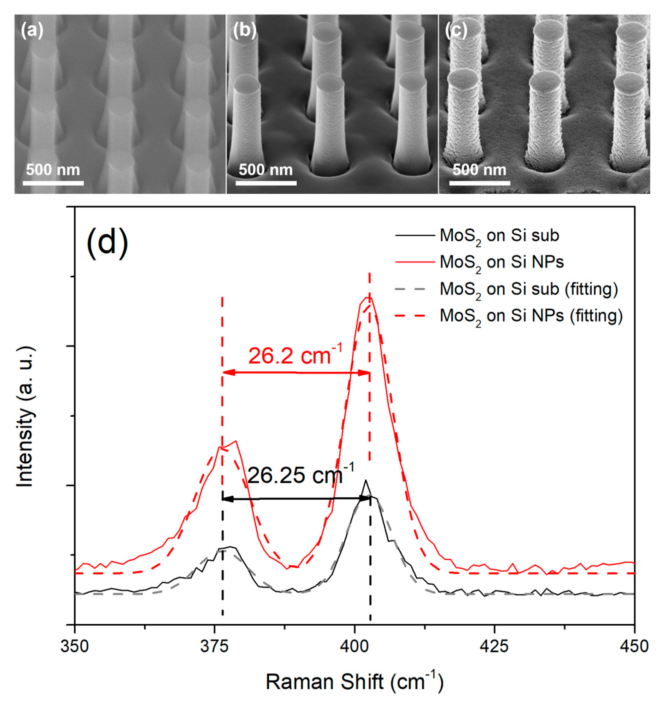
Figure 3.
Mo 3d (a) and S 2p (b) core level XPS spectra of planar MoS2 thin film and Si/MoS2 core/shell NP arrays.
Figure 3.
Mo 3d (a) and S 2p (b) core level XPS spectra of planar MoS2 thin film and Si/MoS2 core/shell NP arrays.
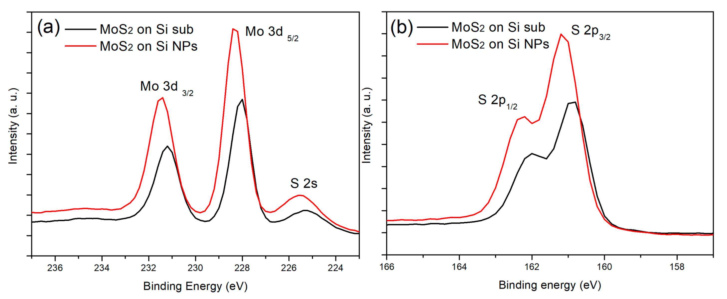
Figure 4.
Surface-enhanced Raman scattering (SERS) signals of the R6G molecules (1 mM) on the Si, MoS2 thin film, and Si/MoS2 core-shell NP arrays substrates.
Figure 4.
Surface-enhanced Raman scattering (SERS) signals of the R6G molecules (1 mM) on the Si, MoS2 thin film, and Si/MoS2 core-shell NP arrays substrates.
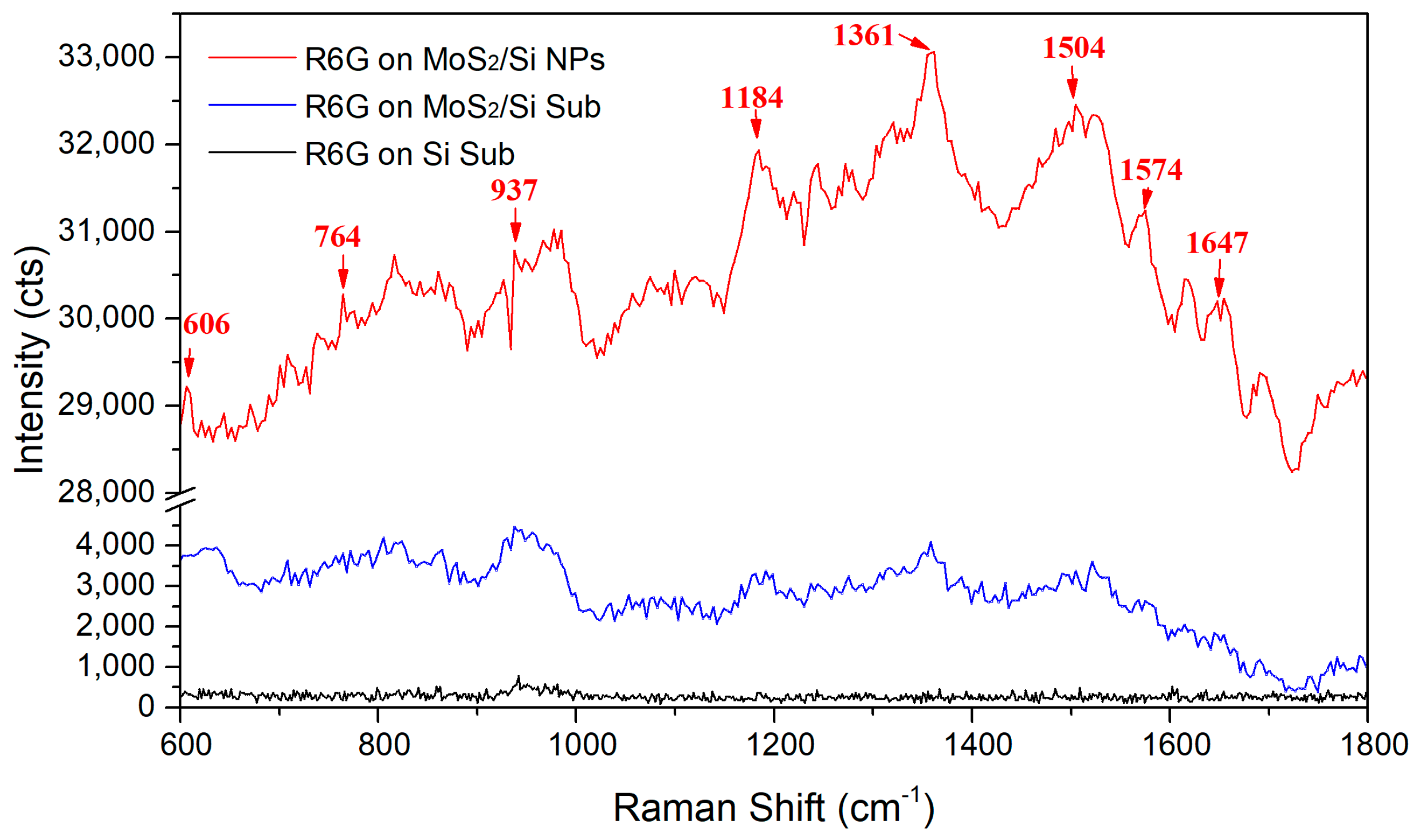
Figure 5.
Band diagram schematic of charge transfer (CT) process between R6G molecule and Si/MoS2 core-shell NP.
Figure 5.
Band diagram schematic of charge transfer (CT) process between R6G molecule and Si/MoS2 core-shell NP.
Publisher’s Note: MDPI stays neutral with regard to jurisdictional claims in published maps and institutional affiliations. |
© 2021 by the authors. Licensee MDPI, Basel, Switzerland. This article is an open access article distributed under the terms and conditions of the Creative Commons Attribution (CC BY) license (http://creativecommons.org/licenses/by/4.0/).
Share and Cite
MDPI and ACS Style
Ko, T.-S.; Liu, H.-Y.; Shieh, J.; Shieh, D.; Chen, S.-H.; Chen, Y.-L.; Lin, E.-T. Using Si/MoS2 Core-Shell Nanopillar Arrays Enhances SERS Signal. Nanomaterials 2021, 11, 733. https://doi.org/10.3390/nano11030733
AMA Style
Ko T-S, Liu H-Y, Shieh J, Shieh D, Chen S-H, Chen Y-L, Lin E-T. Using Si/MoS2 Core-Shell Nanopillar Arrays Enhances SERS Signal. Nanomaterials. 2021; 11(3):733. https://doi.org/10.3390/nano11030733
Chicago/Turabian StyleKo, Tsung-Shine, Han-Yuan Liu, Jiann Shieh, De Shieh, Szu-Hung Chen, Yen-Lun Chen, and En-Ting Lin. 2021. "Using Si/MoS2 Core-Shell Nanopillar Arrays Enhances SERS Signal" Nanomaterials 11, no. 3: 733. https://doi.org/10.3390/nano11030733
Note that from the first issue of 2016, this journal uses article numbers instead of page numbers. See further details here.