1. Introduction
Stencil computations invariably need large volumes of data, which have to be fetched from external memory, typically some form of external dynamic memory. In recent years, high-end Field-Programmable Gate Array (FPGA)-based computers have been shown to offer excellent performance and excellent energy efficiency as specialized co-processors. A typical usage of these FPGA-based co-processors is for streaming computations, in which data arrives sequentially, typically from a computer network. However, for stencil computations the external memory accesses, in addition to the sequential component, have other patterns as well. These may range from accessing columns or diagonals of matrices to accessing less regular patterns. Vector supercomputers of the 1970s–1990s, such as the Cray-1, Cray-2, CDC-205, Fujitsu VP2600/10, NEC SX series, Convey C1, etc., supported fast memory accesses with “strides”, i.e., fixed distances in the memory between accesses, as these are needed for matrix column and matrix diagonal accesses; however, these machines had static memory with fixed access time and non-dynamic memory. Such machines also supported “gather-scatter” operations, i.e., operations in which sequential accesses were in locations found within a vector register. Last but not least, such machines had a clock frequency around 100–200 MHz (approximately 80 MHz for the Cray-1 and getting faster in every generation).
As the technology has advanced, and nowadays FPGA supercomputers are aimed at the solution of some problems for which vector computers were used a few decades ago (e.g., computational fluid dynamics), it is worth revisiting the issue of main memory access. Is this particular problem solved, or, due to issues stemming from technology differences—and specifically from the different memory access time disparity and the external memory being dynamic and not static—should one hand-code memory accesses? In addition, memory access times are published by FPGA hybrid computer vendors for access patterns which demonstrate maximum capabilities, which may or may not apply to a user’s needs.
The contributions of this work are:
An experimental evaluation of the main memory subsystem of a high-end FPGA-based hybrid computer, namely the Convey HC-2ex under several access pattern scenarios, and
A comparison of the vendor-supported memory access through the (sophisticated) memory controller vs. hand-coded memory access sequencing and access aggregation for an application which does not have simple strides, namely Zuker’s algorithm for bioinformatics.
The aim of this work is to provide quantitative results which will aid the designer in organizing his/her memory data access code. The experimental measurements are both for single accesses in which the latency dominates and burst accesses which are handled by the controller. The purpose of this work is expressly to assess whether the vendor-provided memory access mechanisms are advantageous vs. hand-coded memory accesses. For this reason, the gather-scatter mechanisms which are very useful in dealing with very sparse matrices and other highly irregular data are not considered, as it is evident that the complete lack of structure would not give any incentive to the programmer to proceed with hand-coding, whereas the case studies that we have evaluated do have some structure which a smart memory controller could unveil.
The remainder of this paper is as follows:
Section 2 has a brief description of related work.
Section 3 briefly presents the Convey HC-x architecture, in order for the reader to understand the way in which the vendor-supported memory controllers work, and what is needed for the user to organize data in the memory.
Section 4 is the main section with measurements of the Convey HC-2ex memory, and
Section 5 has a comparison of the Convey memory controller performance vs. hand-coding of memory accesses for the Zuker bioinformatics algorithm, which does not have very straightforward access patterns. Finally,
Section 6 has conclusions from this work.
2. Related Work
So far there exist studies which compare high-end FPGA-based computers such as the HC-x architecture against Central Processing Unit (CPU) and Graphics Processing Unit (GPU) performance and energy efficiency on different benchmarks. Bakos [
1] was the first who focused on the comparison of the Convey HC-x with CPU and GPU. In his investigation different benchmarks such as double precision floating point operations or single precision multiplies were performed. The results showed that the Convey HC-1 outperforms the Xeon 5520 only in benchmarks that need strides in memory. In other benchmarks with floating point operations, Nvidia GPUs and even CPUs such as the Intel Xeon outperform the Convey HC-1.
Jones et al. [
2] and Luk et al. [
3] also investigated the same comparison with similar results. In their research, they used benchmarks that have different memory access patterns (different locality). Their results indicate that HC-1 and GPU outperform CPU for all their benchmarks. The main conclusion of their research is that GPUs perform faster than HC-1 in streaming applications. On the other hand, HC-1 is faster and more energy efficient from GPUs for applications that need non-sequential memory accesses [
3].
Nagar and Bakos [
4] performed an implementation for a double precision floating point sparse matrix-vector multiplier on the Convey HC-1. They also presented an improved FPGA architecture for floating point accumulation and integrated this with the Convey HC-1. Their results showed that the performance of the Convey is better than the performance of the Tesla S1070 GPU in most cases. However, the Convey HC-1 has limits in memory interconnection with FPGAs and as a result the implementation cannot be scaled arbitrarily. Weisz et al. [
5], Maas et al. [
6] and Jin [
7] have also studied the memory subsystem of the Convey HC-1 and HC-2(ex).
3. Convey HC-x Architecture
The Convey Computer Company (in their own words) introduces an innovative new way of obtaining extreme performance for High Performance Computing (HPC) applications: hybrid-core computing. Hybrid-core computing is based on an asymmetric architecture that combines the economies and programmability of industry standard processors with the performance and efficiency of a hardware-based, application-specific design. The Convey HC-x series includes a scalar instruction set, a cache coherent connection to the host processor, and a high-bandwidth local memory system. The coprocessor memory subsystem supports virtual-to-physical translation such that host memory and coprocessor memory references can be mapped in a single process “address space”.
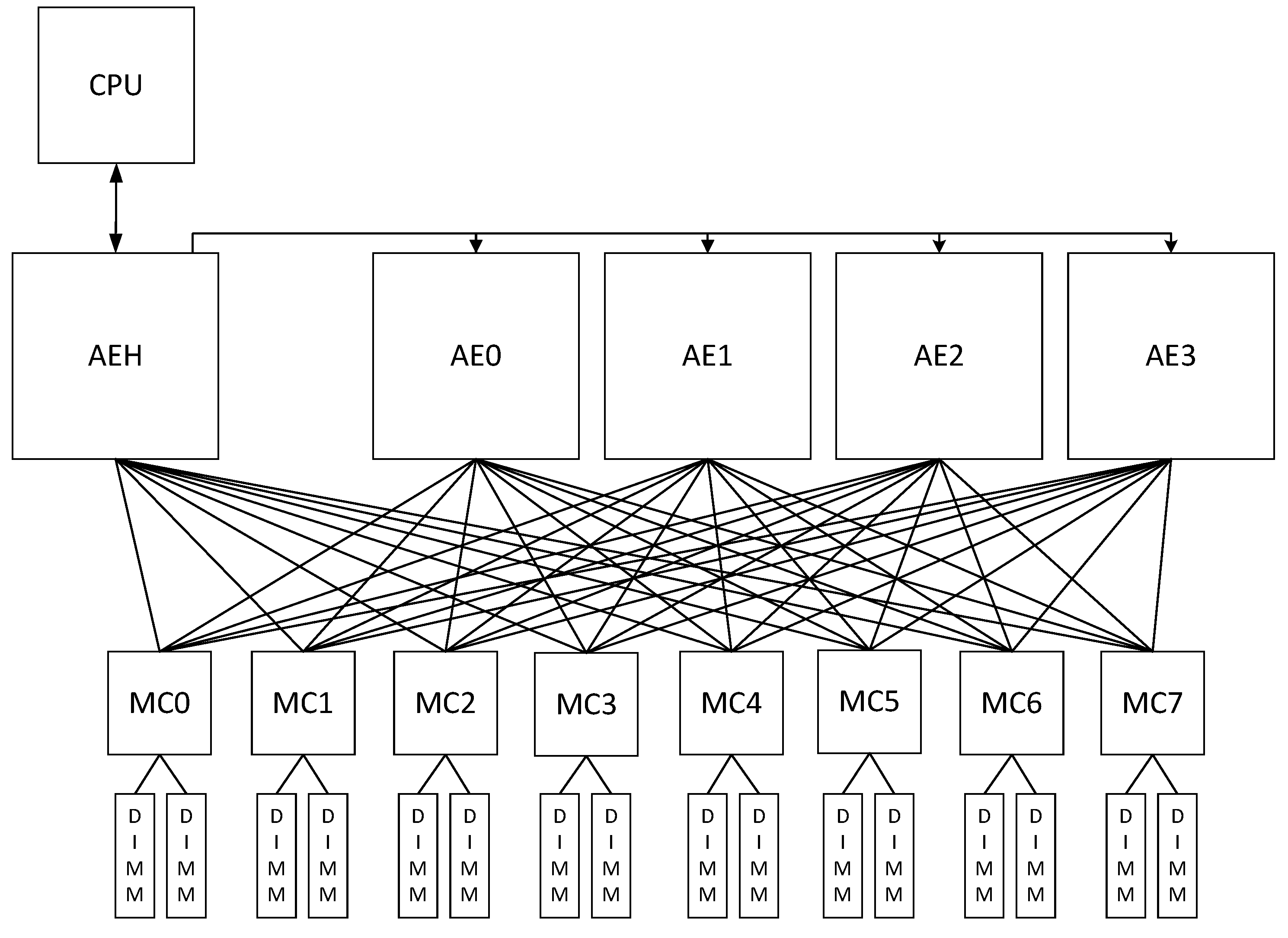
Convey’s hybrid-core technology is an example of a High Performance Reconfigurable Computer (HPRC) system that achieves a compromise between application-specific hardware and architectural integration. The Convey hybrid-core server, HC-2ex, has access to two pools of physical memory: the host memory pool with up to 128 GB of physical memory, located on the x86 motherboard, and the coprocessor memory pool with up to 128 GB of memory, located on the coprocessor board. The coprocessor contains three main components: the Application Engine Hub (AEH), the Memory Controllers (MCs), and the Application Engines (AEs).
Each Application Engine is connected to all eight memory controllers via a network of point-to-point links to provide high sustained bandwidth without a cache hierarchy. Each Memory Controller is physically connecting to one-eighth of the coprocessor memory through a 300 MHz DDR memory link. Each Memory Controller is divided in two Dual In-line Memory Modules (DIMMs) and these ports are clocked at 150 MHz. In fact, the available channels to the memory are 16 channels at 150 MHz each.
The interface of the crossbar, which is provided by the Convey HC-x, connects each AE with all MCs, as shown in
Figure 1. The crossbar decodes the address requests and allows the AEs to maintain an abstract idea for the allocation of data in the memory.
From
Figure 1 and the memory access bandwidth described above, it is obvious that streaming applications have abundant bandwidth. However, stencil computations have more complex patterns, which need to be evaluated, as described in
Section 4.
4. Experimental Memory Subsystem Evaluation
The Convey architecture, as shown in
Section 3, encompasses a sophisticated Memory Controller. It is therefore useful to ascertain the memory subsystem performance in different usage scenarios. The performance of any system of this nature is affected by several parameters. The most important parameter is the way in which the memory subsystem communicates with the remaining system, such as the x86 processor and the FPGA coprocessor. The communication part in the coprocessor end is of great importance in our research.
The advantage of this hybrid super-computer, as it is presented by Convey Computers, is the memory subsystem of the co-processor. The memory subsystem consists of two parts, the DDR2 memory and eight MCs with two ports to memory each.
Previous research in memory systems showed that there are two critical parameters affecting the performance, the latency and the bandwidth of memory. We performed a series of experiments to verify the communication between the memory and coprocessor (AEs) as shown in the Convey manuals. The Convey manuals and, more specifically, the Personality Development Kit (PDK) Reference manual [
8] provide the theoretical values of bandwidth that the Convey could achieve according to the capability of DDR2. However, the requirements to achieve those values are very constraining to the designer. All AEs have to send requests to the memory from every MC’s ports on every clock cycle without any MC stalls. One of the provided interleave schemes must be used to optimally distribute memory requests among the MCs, DIMMs and banks. These requirements are almost impossible to integrate in a common algorithm hardware design. Furthermore, the interface of the crossbar overloads the system with additional delays.
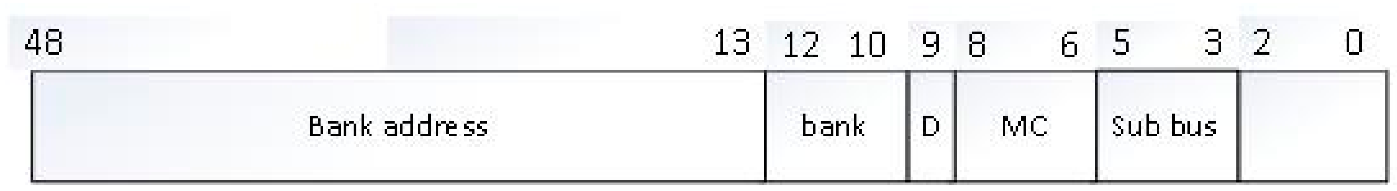
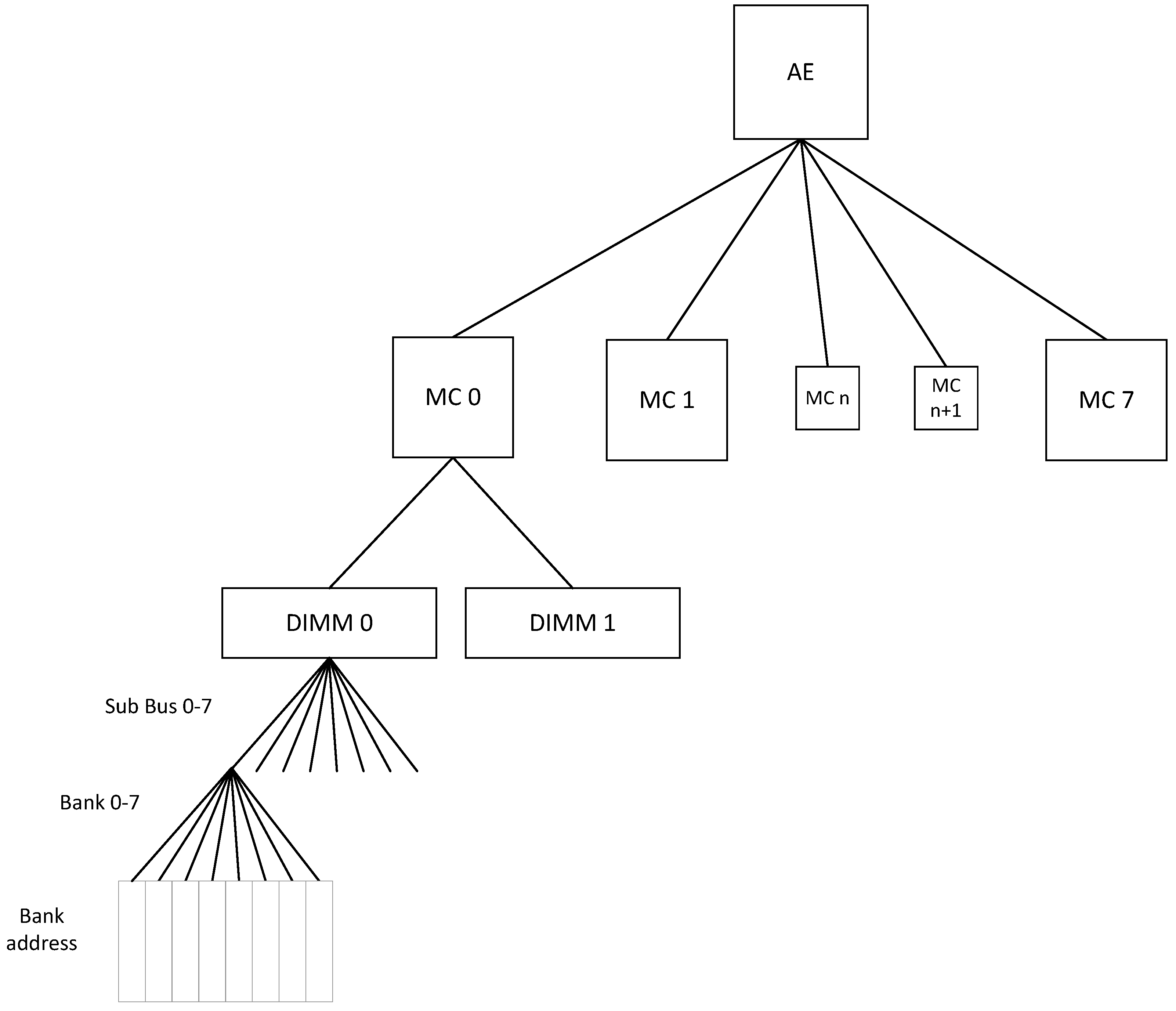
Figure 2 shows the binary interleave scheme which is used by Convey, whereas
Figure 3 shows the hierarchy itself. From the combination of these two figures we can glean how the designer needs to place the application data in the memory space in order for overlapping accesses to not conflict. The least significant bits are for byte addressing of the 64-bit word. Subsequently there are three bits for the “Sub bus”, three bits for the Memory Controller, one bit which chooses odd/even DIMM, and three bits for the Memory Bank. The comparison of
Figure 2 and
Figure 3 shows how the user’s address space gets mapped to actual DIMM circuits of DDR2 memory.
The methodology of our experiments is governed by specific rules. All measurements are repeated 1000 times and the results presented are the average number. In our experiments we used only one of the AEs but we can easily argue that our results extend proportionally in the whole system. The clock in our designs is bounded from the clock of MC ports which runs at 150 MHz.
Our work focuses mainly on the performance between the coprocessor memory and the coprocessor itself. The experimental testbed comprises three parts: the DDR2 memory, the eight MCs and the four AEs. The two figures of merit which are of interest are the bandwidth and the latency of the Convey HC-x memory subsystem.
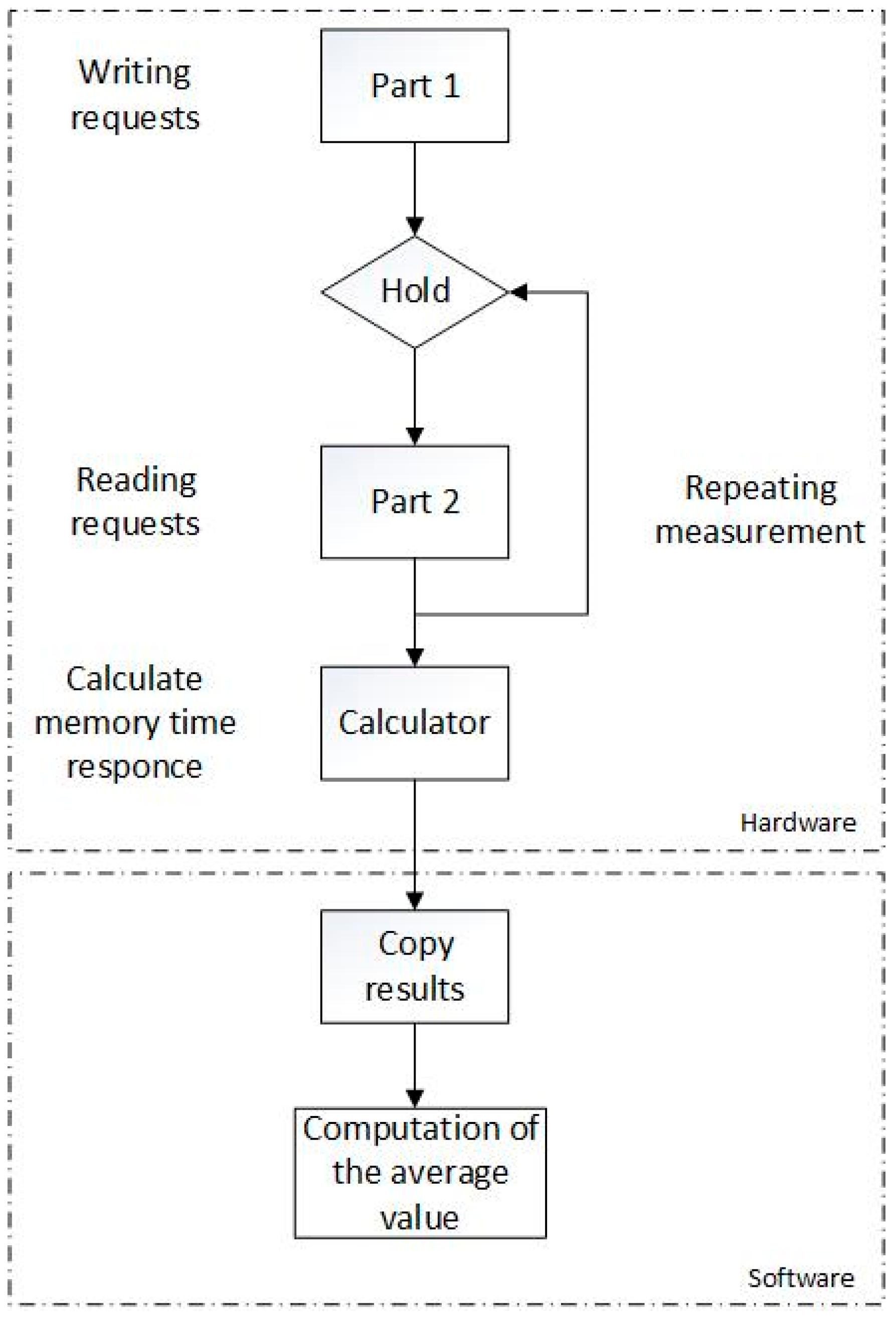
Our experimental setup consists of a hardware design that takes measurements of the bandwidth and latency of the memory subsystem on a coprocessor, and the way in which the measurements are made is shown in
Figure 4.
4.1. Latency Experiments
The initial experiments measure the latency of the memory subsystem. The latency is calculated by the time that an AE takes to send a read request to the memory and the requested data reach the AE. In the first experiment, latencies for random requests are measured. Our hardware design consists of two parts. In the first part our design sends several writing requests to the memory, which writes random numbers to different memory locations. The random number generator was also implemented in the hardware on the AEs. Each write request in the memory is independent and differs in memory location in order to test if locality affects the latency. In our experiments, four different sequences of addresses of writing requests were used, namely eight to 64 bytes, 64–1024 bytes, 1024–8192 bytes and >8192 bytes.
In the second part of this experiment, the design sends read requests to the memory, which are the same addresses written in the first part of the design. The response time of the memory subsystem for all read requests is measured by a counter that also checks if the data reads are the same with those written in the first part of the experiment. This measurement is repeated 1000 times and the average value is calculated by the software.
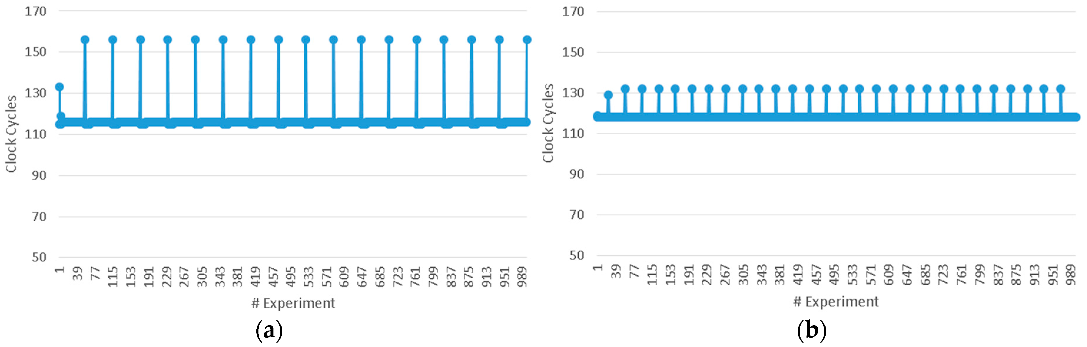
The average latency measured is 720 ns or 120 clock cycles. In order to present the results of the experiments, two typical examples of the measurements of latency are shown in
Figure 5a,b. In the first example, one MC is used for each series of experiments and their data addresses differ 64–1024 bytes, as shown in
Figure 5a.
Figure 5b shows the second example in which four MCs are used and their data addresses differ by 8–64 bytes. From the results it is deduced that the locality of data is reflected both in latency and in the variance of latency.
The latency of the memory subsystem varies through the experiments. The variance of the latency in our measurements is affected by the number of MCs used and the data location of the read requests in the memory. From the results it is assumed that in each measure of the experiment, when the addresses of the data read are between 8–64 bytes apart, the variance of the latency is quite low, as shown in
Figure 6a. On the contrary, when the requested data are in other DIMMs and served by a different MC port, the latency and the variance of latency are increased, as shown in
Figure 6b. From
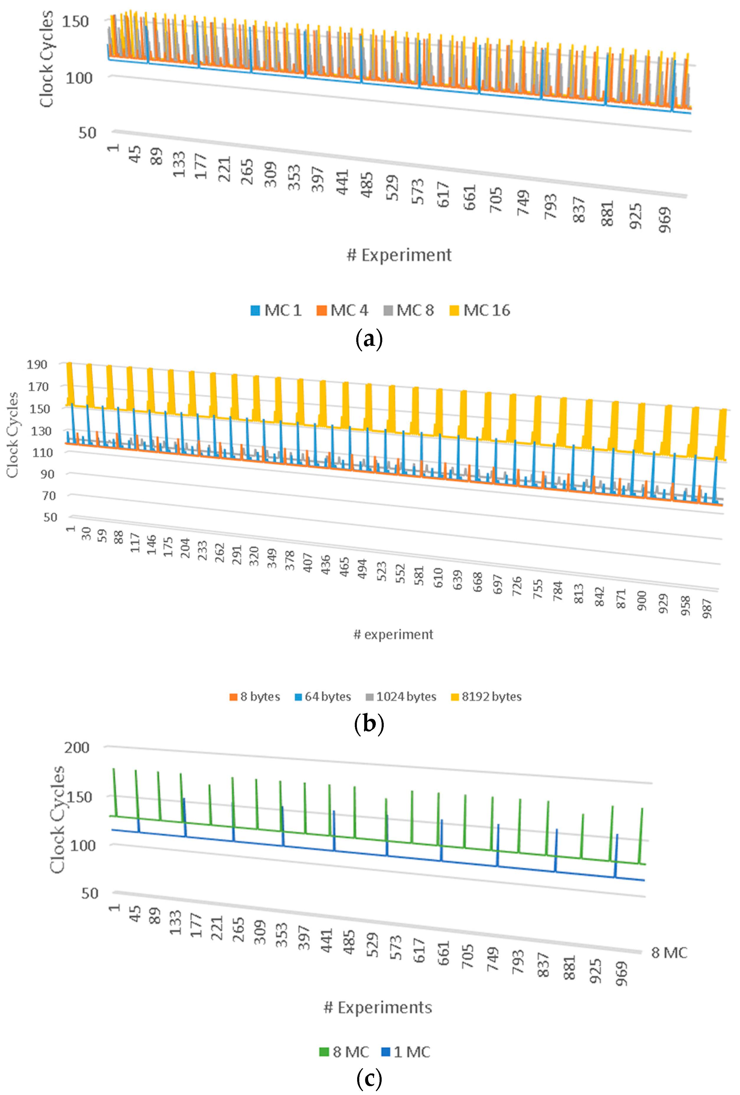
Figure 6a it is deduced that the addresses of the data reads are in the same DIMM and the latency is about 120 clock cycles, except for some peaks (of 160 clock cycles). Increased peaks appear due to stalls of MCs and show a further increase as the used MCs are increased.
Figure 6c shows that the latency is increased to 130 clock cycles, while peaks show a higher density. It also shown that the number of MCs affects the variance of latency; increased numbers of MCs results in an increase in the variance of the latency.
This number is extremely big, considering that we need new piece of data in every clock cycle in order to develop an efficient hardware design which could compare with designs in CPU or GPU in performance. The memory subsystem of the Convey HC-x is built for a large amount of memory requests and it has the ability to hide this latency. Knowing how the memory DDR2 integrated circuits work, we can claim that the MCs do some kind of buffering. The most likely scenario of buffering is that MCs hold in their buffers the whole block of each DIMM that is used each time. So we could suppose that if an AE is continuously sending requests for data in the same block of memory, the MC will respond quickly, thus hiding the latency. We tested this assumption in our subsequent experiments, in order to measure the bandwidth of the memory subsystem.
4.2. Bandwidth Experiments
The second important feature of the memory being measured is the bandwidth. The following experiments were conducted to measure the bandwidth for different data structures using different numbers of memory ports.
Two kinds of experiments were performed for reading burst data from the memory. The first sends a different number of reading requests to the memory and calculates the response time using only one memory port. The second one uses multiple ports to access the memory and calculates the response time as well.
The experiments were repeated for datasets of 1, 5, 10 and 50 MB.
4.2.1. Burst Data
In the first type of experiment, the response time of the memory was measured for three different numbers of reading requests, all using a single MC port to access memory. The requested data are in burst mode, and the addresses of subsequent requests differ by eight bytes. So the AE sends reading requests in all DIMMs. This happens because in our design we use the interface to the crossbar which allows one MC port of the hardware design to access all of the memory’s DIMMs. The use of the crossbar is possible to add some delay to our measurements, which could be increased when more memory ports are in use. In each measurement the MC port feeds the AE with approximately one requested datum in every clock cycle. Additionally, the AE sends many requests and the ratio of the data requests and the MC port response time is converging to one, i.e., the theoretical upper bound is actually reached for well-balanced burst-type accesses.
Table 1 shows that the measured bandwidth of the memory is 1.2 GB/s when only a single memory port is used. In contrast, the theoretical bandwidth of DDR2 is 2.5 GB/s according to the Convey HC-x manual. Hence we conclude that with a single port we can expect half of the maximum bandwidth, and this is what the experimental evaluation demonstrates. We can expect that the bandwidth of 2.5 GB/s would be reached if the AE sends requests from both ports of the MC. The reason why we measured a single port in this experiment is that in a typical user’s code, the requests may not be sufficiently “convenient” to use both ports in every cycle; however, it can be expected that one piece of data will be needed per cycle in a deeply pipelined design, such as stencil computing. We also note that the maximum bandwidth is achieved even in short bursts.
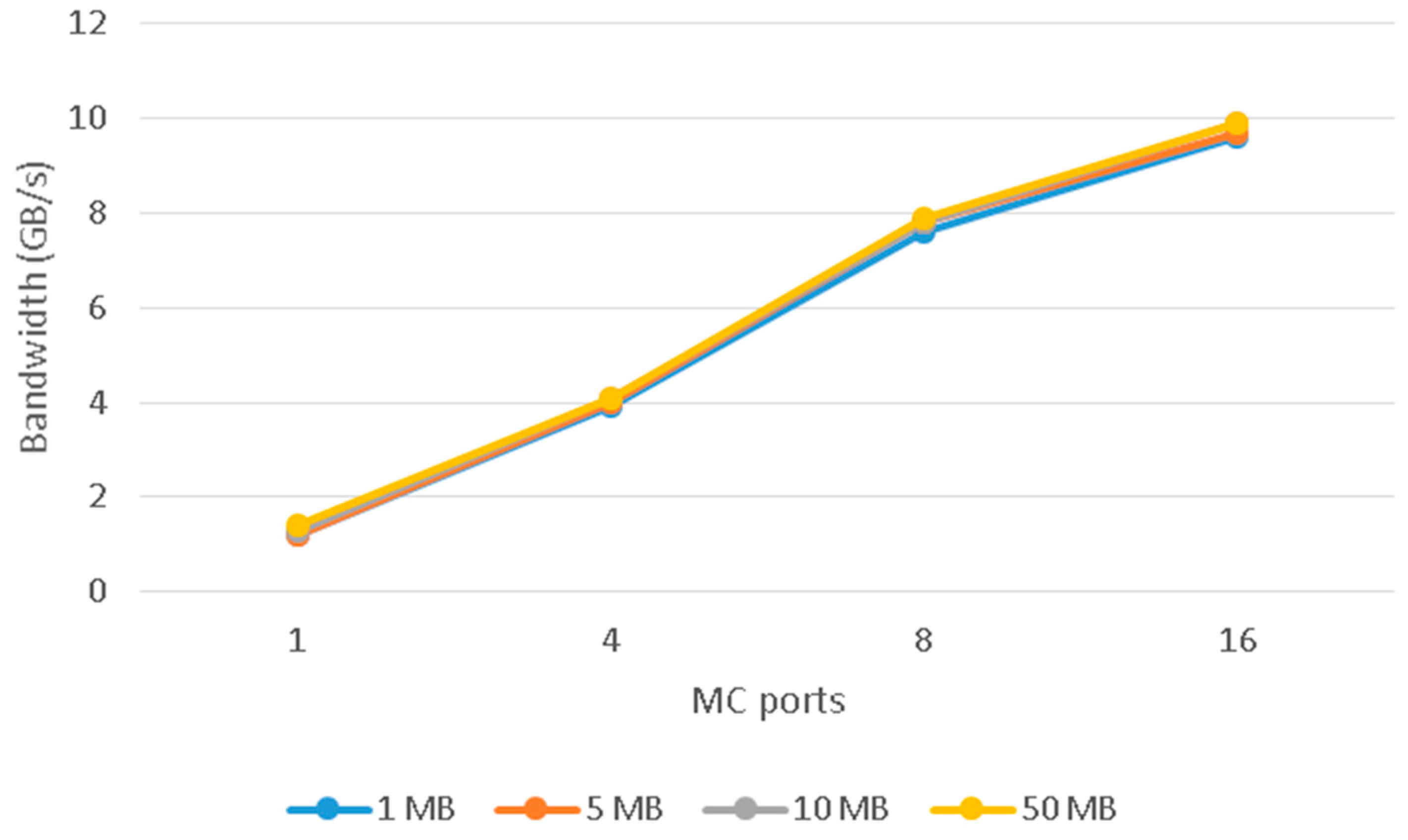
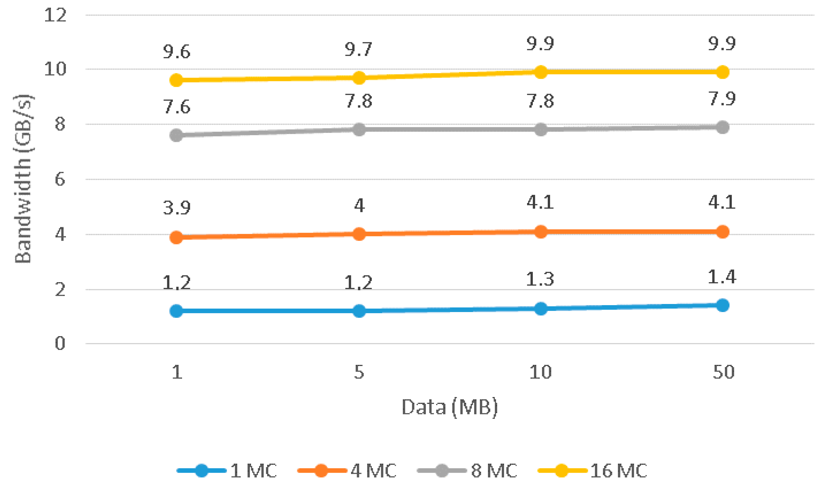
In the second burst experiment, a different number of memory ports are used to read in burst mode. In this group of measurements, the AE uses the interface of the crossbar and therefore all memory ports have access to all memory DIMMs. The bandwidth was expected (or at least it would be desirable) to increase linearly as the number of the MC ports was increasing. A linear increase of bandwidth will be close to the theoretical bandwidth of the DDR2 memory. In the results of this experiment, shown in
Table 2 and
Figure 7, we note that the memory bandwidth indeed increases as the number of MC ports used increases. However, the increase was not expected, no matter what dataset is used, as shown in
Figure 8.
The percentage reduction of usable memory bandwidth is caused by two reasons:
The requested data from each port are in consecutive addresses in the memory and as a result every MC port requests data from all DIMMs. Many stalls and collisions appear from this fact.
Our hardware design uses one Finite-State Machine (FSM) to control all MC ports. As a result, when a MC port is stalled, the other ports must wait for the stalled ones to be activated again.
When the design uses four MC ports, the result output for bandwidth is 3.9 GB/s instead of the expected theoretical bandwidth of 5 GB/s. When using eight MC ports, the result output is 7.4 GB/s instead of the theoretical bandwidth of 10 GB/s. The peak bandwidth being measured for using 16 MC ports is 9.6 GB/s instead of the expected 20 GB/s. The theoretical bandwidth could be achieved if the hardware design uses one FSM for each MC port which would send reading requests independently from stalls and collisions of other MC ports. Each MC port must send read requests to a different DIMM even though the design uses the interface of the crossbar.
The above experiment reveals that the memory bandwidth, which can be achieved for a realistic user code without too many considerations, is a good fraction of the maximum theoretical bandwidth; however, in order to cover the performance gap from the “quite good with no worries” performance to the “squeeze every byte out of the bandwidth” performance, the designer’s task is not trivial, as he/she cannot always know what conflicts are generated inside the Memory Controller vis-à-vis other requests which arrive from different AEs.
4.2.2. Data Strides
Experiments were also performed for other data structures involving data strides. Different strides were tested to measure the bandwidth of the memory. Our goal was to find the limits of the MC port in reading request data with strides. Previous work showed an efficient performance of the Convey HC-x for benchmarks with strides in memory. In our experimental study, different memory strides were tested in order to measure the bandwidth. The 512-byte stride is the bound of the memory port for an efficient hardware design as shown in
Table 3. The first three measurements for strides, namely 8, 64 and 512 bytes, showed that the MC port and the whole memory subsystem serve the AE requests as fast as with sequential burst accesses. The use of one MC port for these strides feeds the AE with different data in almost every clock cycle. The AE uses the interface of the crossbar and as a result the MC port has access to all DIMMs. However, for bigger strides, which would make sequential accesses all go to a single DIMM, namely for strides of 1024 and 8192 bytes, the bandwidth is dramatically reduced, as expected. This is a very obvious issue, known for many decades, and there are solutions dating back to the 1980s in order to address it (e.g., adding a “dummy” memory column to a matrix). The important results from these measurements are that when strides get mapped to different DIMMs, the performance is identical to sequential burst memory accesses, and the MCs do a good job in this case.
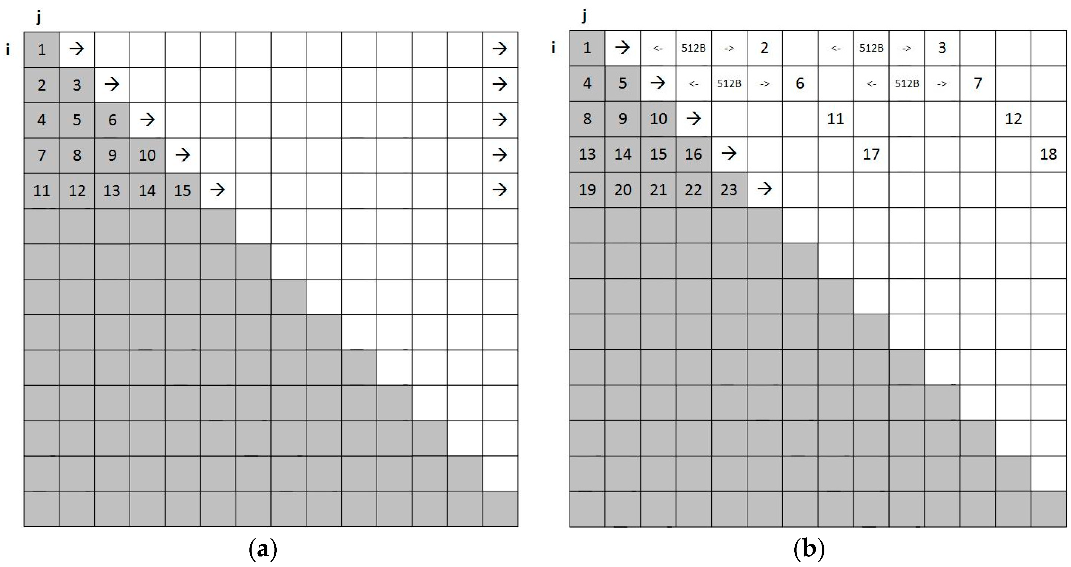
5. Triangular Data Structures
The last one of our experiments was a comparison between hand-coded memory accesses vs. memory accesses from code produced by the vendor’s tools. For this experiment we used a well-known algorithm from bioinformatics, Zuker’s algorithm. The prediction of the RNA secondary structure is a challenging task in computational biology. The methodology of Zuker’s UNAFold algorithm has been introduced to contribute to this task. The analysis of Zuker’s UNAFold algorithm was the motivation for the study of memory response time for different data structures such as triangular tables [
9,
10]. Multiple accesses from large triangular matrices are required for the calculation of the algorithm.
Our experiments aim to measure the efficiency of MC ports in structures that need irregular accesses in memory. In the present study, two techniques of reading data of a triangular matrix are proposed. In both techniques the design uses one MC port to read the entire matrix.
In the first technique, our design sends read requests only for the data of the lower triangular table and measures the time response of the memory subsystem.
Using the results of the measurements for data accesses, a technique is proposed where the design sends read requests needed for the lower triangular table memory accesses in smaller address increments, namely 512 bytes.
These two experiments are shown in
Figure 9a,b, respectively. We note by observing these figures that the access patterns in
Figure 5a are not comprised of strides in the classical sense (e.g., when we want to access the diagonal of a m × n matrix the stride is fixed to m + 1 words). Rather, we have sequential accesses of different sizes each. In
Figure 9b we have a data placement which is similar to a stride, as we place some of the data in addresses differing by 512 bytes.
In these experiments two different sizes of matrices were used, namely 0.1 and 0.7 GB. The purpose of our measurements is to read only the data of the lower triangular matrix as fast as possible. The bandwidth that the MC port succeeds is 1.2 GB/s in both techniques for both matrix sizes. However, the first technique is a bit faster. This means that the MC port “feeds” the AE with new data in every clock cycle. The results show that the memory subsystem responds efficiently in these data structures and there is no need for additional intervention in the way of reading the data from the designer.
In order to evaluate how hand-coded designs would fare vs. the vendor-supported MCs, we conducted an additional series of experiments, in which FSMs in the AEs would schedule the memory accesses. These designs actually performed worse than those with the vendors’ tools (after several refinements the results were close to the ones reported above, but still they were worse). We believe that there are two reasons: the controller seems to do some caching of fetched data, and this was lost in the user’s code; also, the controller can schedule requests around conflicts and serialize the requests in order to deliver data to the user. Both of these features were lost, whereas in fact the user code may have inadvertently caused conflicts which reduced the performance.
6. Conclusions
In this work we performed an extensive experimental evaluation of the Convey HC-x architecture memory subsystem, using a Convey HC-2ex hybrid FPGA supercomputer. The experiments were for both random and burst accesses, and showed that the vendor-provided memory controller takes good advantage of the memory subsystem capabilities, that the hierarchy with odd/even banks of DIMMs works together with multiple ports, and the “sub-banks” concept and the actual interleave banks deliver for many cases almost all of the memory bandwidth, even when a single port is used. In addition, the memory controllers do a good job in sequencing and caching requests, as shown by the experiment in which manually scheduling memory requests performed no better than the vendor-produced code.
Acknowledgments
This work was partially funded by the following projects: EU H2020 project “COSSIM-Novel, Comprehensible, Ultra-Fast, Security-Aware CPS Simulator”, Project Reference 644042, under the ICT-01-2014 call if the RIA-Research and Innovation Action, and, by the General Secretariat of Research and Technology of Greece (GSRT) under the project “AFORMI-Allowing for Reconfigurable Hardware to Efficiently Implement Algorithms of Multidisciplinary Importance”, funded in the call “ARISTEIA” of the framework “Education and Lifelong Learning”, with code 2427.
Author Contributions
Initial work on how data structures map to memory access patterns was performed by A. Dollas and I. Papaefstathiou under the project AFORMI. This work was continued by the same authors under project COSSIM, in which the study was done expressly towards speeding up simulators with high-end hybrid reconfigurable processors. The codes to test the memory subsystem under various access pattern scenarios were developed by the first author, K. Kalaitzis, who also conducted the experiments. The second author, E. Sotiriadis, participated in the code development and provided expert help in solving technical problems on the Convey HC-2ex. The entire project was supervised by A. Dollas and I. Papaefstathiou.
Conflicts of Interest
The authors declare no conflict of interest.
References
- Bakos, J.D. High-performance heterogeneous computing with the Convey HC-1. Comput. Sci. Eng. 2010, 12, 80–87. [Google Scholar] [CrossRef]
- Jones, D.H.; Powell, A.; Bouganis, C.-S.; Cheung, P.Y.K. GPU versus FPGA for high productivity computing. In Proceedings of the 2010 International Conference on Field Programmable Logic and Applications (FPL), Milano, Italy, 31 August–2 September 2010.
- Betkaoui, B.; Thomas, D.B.; Luk, W. Comparing performance and energy efficiency of FPGAs and GPUs for high productivity computing. In Proceedings of the 2010 International Conference on Field-Programmable Technology (FPT), Beijing, China, 8–10 December 2010.
- Nagar, K.K.; Bakos, J.D. A sparse matrix personality for the convey HC-1. In Proceedings of the 2011 IEEE 19th Annual International Symposium on Field-Programmable Custom Computing Machines (FCCM), Salt Lake City, UT, USA, 1–3 May 2011.
- Weisz, G.; Melber, J.; Wang, Y.; Fleming, K.; Nurvitadhi, E.; Hoe, J.C. A Study of Pointer-Chasing Performance on Shared-Memory Processor-FPGA Systems. In Proceedings of the 2016 ACM/SIGDA International Symposium on Field-Programmable Gate Arrays, Monterey, CA, USA, 21–23 February 2016.
- Maas, M.; Love, E.; Stefanov, E.; Tiwari, M.; Shi, E.; Asanovi, K.; Kubiatowicz, J.; Song, D. A high-performance oblivious RAM controller on the convey HC-2ex heterogeneous computing platform. In Proceedings of the Workshop on the Intersections of Computer Architecture and Reconfigurable Logic (CARL), Davis, CA, USA, 7 December 2013.
- Jin, Z. Memory Interface Synthesis for FPGA-Based Computing. Ph.D. Thesis, University of South Carolina, Columbia, SC, USA, 8 September 2014. [Google Scholar]
- Convey. Convey Personality Development Kit Reference Manual; Version 5.2; Convey Computer: Richardson, TX, USA, 2012. [Google Scholar]
- Zuker, M.; Patrick, S. Optimal computer folding of large RNA sequences using thermodynamics and auxiliary information. Nucleic Acids Res. 1981, 9, 133–148. [Google Scholar] [CrossRef] [PubMed]
- Markham, N.R.; Michael, Z. UNAFold. In Bioinformatics; Humana Press: Totowa, NJ, USA, 2008; pp. 3–31. [Google Scholar]
© 2016 by the authors; licensee MDPI, Basel, Switzerland. This article is an open access article distributed under the terms and conditions of the Creative Commons Attribution (CC-BY) license (http://creativecommons.org/licenses/by/4.0/).


