Article

The Electronic Properties of Silicon Nanowires during Their Dissolution under Simulated Physiological Conditions

1
Institute of Electron Devices and Circuits, Ulm University, 89081 Ulm, Germany
2
Institute of Analytical and Bioanalytical Chemistry, Ulm University, 89081 Ulm, Germany
3
Electron Microscopy of Materials Science, Ulm University, 89081 Ulm, Germany
*
Authors to whom correspondence should be addressed.
Current address: Division of Biomaterials and Regenerative Medicine, Department of Medical Biochemistry and Biophysics, Karolinska Institutet, 171 77 Stockholm, Sweden.
Current address: Department of Cellular Biophysics, Max Planck Institute for Medical Research, 70569 Stuttgart, Germany.
§
Current address: Microsystems Technology Group, Ilmenau University of Technology, 98693 Ilmenau, Germany.
Appl. Sci. 2019, 9(4), 804; https://doi.org/10.3390/app9040804
Submission received: 20 December 2018 / Revised: 8 February 2019 / Accepted: 20 February 2019 / Published: 25 February 2019
(This article belongs to the Special Issue Silicon Nanowires and Their Applications)

Abstract

:

Featured Application

The present results have implications for the long-term usage of silicon nanowire-based field-effect transistors as biochemical sensing devices.

Abstract

Silicon nanowires are considered promising future biomedical sensors. However, their limited stability under physiological conditions poses a challenge in sensor development and necessitates a significantly improved knowledge of underlying effects as well as new solutions to enhance silicon nanowire durability. In the present study, we deduced the dissolution rates of silicon nanowires under simulated physiological conditions from atomic force microscopy measurements. We correlated the relevant change in nanowire diameter to changes in the electronic properties by examining the I-V characteristics of kinked silicon nanowire p–n junctions. Contact potential difference measurements and ambient pressure photoemission spectroscopy additionally gave insights into the electronic surface band structure. During the first week of immersion, the Fermi level of n-type silicon nanowires shifted considerably to higher energies, partly even above the conduction band edge, which manifested in an increased conductivity. After about a week, the Fermi level stabilized and the conductivity decreased consistently with the decreasing diameter caused by continuous nanowire dissolution. Our results show that a physiological environment can substantially affect the surface band structure of silicon nanowire devices, and with it, their electronic properties. Therefore, it is necessary to study these effects and find strategies to gain reliable biomedical sensors.

Graphical Abstract

1. Introduction

Silicon nanowires (SiNWs) have emerged as promising nanoscale transducers for biomedical sensor applications [1,2]. Several studies demonstrate the exceptional sensitivity and versatility of ion-sensitive and ion-selective nanowire field-effect-transistors (FETs) combined with the overall compatibility with conventional metal-oxide-semiconductor (CMOS) technologies [3,4,5,6,7]. However, the physiological environment that is prevalent for said biomedical sensing applications presents challenges to materials scientists. The insulating silicon oxide that typically encapsulates silicon nanowires and that is in principle required for a FET configuration dissolves slowly in aqueous solution as siloxane bonds are hydrolyzed [8]. This effect has long been known for silica nanomaterials [9]. Specifically, in an oxygen-containing environment, the underlying nanowire material is consumed as the oxide layer is recovered through oxidation of the interfacial silicon [10]. This degradation of SiNW FETs has recently been described [11] but is often neglected.
In the present study, we therefore took a closer look at the dissolution process and its impact on the electronic properties of SiNWs that are central for any perspective SiNW FET application. I-V measurements of p–n junctions, and the absolute reconstruction of the electronic surface band structure from contact potential difference (CPD) measurements and ambient pressure photoemission spectroscopy (APS), revealed considerable changes in the SiNW surface band structure that were accompanied by an altered SiNW conductivity.

2. Materials and Methods

2.1. Sample Preparation

2.1.1. Kinked p–n Junctions for Measurements of Single SiNWs

SiNWs with an embedded p–n junction for single SiNW dissolution experiments were grown from 50 nm gold nanoparticles (AuNPs; BBInternational, Crumlin, UK) on single-crystalline (100) Si wafer pieces covered by a thermal oxide layer (500 nm). After cleaning with acetone and 2-propanol in an ultrasonic bath for 5 min each, the wafer pieces were subjected to O 2 -plasma treatment ( μ -etch; 5 min, 0.1 torr, 100 Watt). The AuNPs were adsorbed to the surface using poly-l-lysine, which was removed prior to growth through O 2 -plasma treatment as described above. In the SiNW chemical vapor deposition (CVD) set-up, the samples were heated in Ar atmosphere to 475 ° C, after which vapor–liquid–solid (VLS) growth was initiated by introducing 100 sccm SiH 4 /He and 10 sccm H 2 at 75 mbar. The p–n junctions were implemented by admixing the dopant gas and changing it from 20 sccm B 2 H 6 for the p-type branch to PH 3 for the n-type branch during growth. To introduce the kink, this dopant change was accompanied by a sudden drop in pressure [12]. SiNWs grown in this manner have been shown to grow along the <111> axis, thereby exposing {211} and {110} faces on the sides [13,14,15]. The SiNWs were successively transferred from the growth substrate to a chip by releasing them into ethanol (p.a., Merck, Darmstadt, Germany) in an ultrasonic bath and dropwise addition of the resulting dispersion to the respective chip. Then, 100 nm thick Au electrical contacts with 5 nm Ti as adhesive layer were placed by thermal evaporation using electron beam (e-beam) lithography in a lift-off process with polymethyl methacrylate e-beam resist. Previous experiments have shown that thus integrated nanowires with an equivalent level of doping typically show ohmic contact behavior [16].

2.1.2. Samples Densely Covered with SiNWs

The n-type SiNWs for the reconstruction of the surface band structure were grown from an Au layer instead of AuNPs to achieve a high nanowire density on the growth substrate. A 5 nm thick Au layer was deposited on cleansed wafer pieces by thermal (Leybold L560, Köln, Germany) or electron beam evaporation (Temescal FC-1800, Vactec, München, Germany).The layer was dewetted into gold droplets that act as catalyst in the VLS process when heated up in the furnace of the CVD set-up. Admixing 20 sccm PH 3 to the CVD gas mixture over the whole growth phase of the process introduced n-type doping. The CVD process reaction conditions were the same as for the p–n junction nanowires described above and were expected to result in highly doped n-type SiNWs.
The nanowire samples for the study on the Si release were grown at 150 sccm SiH 4 (2% in He), 100 sccm H 2 and a pressure of 100 mbar for 30 min. The growth rate was about 1.5 μ m/min for the given growth parameters. The process resulted in nominally intrinsic SiNW that densely covered the growth substrate.

2.2. Sample Immersion

SiNW samples were immersed at 37 ° C in phosphate buffered saline (PBS at pH 7.2; Prolabo, VWR, Darmstadt, Germany) in polypropylene centrifuge tubes (VWR) to prevent artifacts from silicate that dissolves from glassware. For atomic force microscopy (AFM) and electrical measurements, a 10 mm × 10 mm chip carrying the SiNWs was immersed in 20 mL PBS that was exchanged at least every second day to provide a constant driving force for dissolution, as would be the case for physiological conditions. For CPD and APS measurements, the 10 mm × 10 mm growth substrates with a high density of n-doped SiNWs were immersed in 50 mL PBS and stored at 37 ° C. Here again, the PBS solution was exchanged at least every second day. Before each CPD and APS measurement, the SiNW substrates were rinsed several times with double deionized water to remove the buffer salts, and dried in a nitrogen stream.
ICP-AES measurements were conducted with a Horiba Ultima 2. The samples were diluted with purified water to have the minimum volume of 3 mL for analysis.

2.2.1. Electron Microscopy

Scanning electron microscopy (SEM) was performed using a Zeiss Leo instrument (Zeiss, Oberkochen, Germany) with a sample covered with SiNWs mounted onto a stub holder without further sample preparation.
The transmission electron microscopy (TEM) specimen were prepared by placing drops of the SiNW dispersion onto a lacey carbon 200 mesh Cu grid (Plano, Germany) and letting it dry.TEM analysis was performed using a Philips CM20 transmission electron microscope with thermionic LaB 6 gun at 200 kV and a 1 k × 1 k slow-scan CCD-camera.

2.2.2. Electrical Characterization

A Keithley 4200 SCS parameter analyzer (Tektronix, Germany) was employed for electrical characterization. Each SiNW was sampled three times at each time point in the range from −1.5 V to 1.5 V, with the tungsten needles used to create an electrical contact placed in a different position on the contact pad for each measurement.

2.2.3. AFM Measurements

AFM measurements were conducted using a Digital Instruments Dimension 3100 AFM with Veeco Otespaw probes. Four SiNWs were monitored for 70 days. Each SiNW was scanned over a 10 μ m × 10 μ m area. Data analysis was conducted using Gwyddion 2.44 with its data leveling and profile extracting functions [17]. For each time point of each SiNW, 2–6 profiles were analyzed. Given are the mean values and standard deviations.

2.2.4. Reconstruction of the Nanowire Surface Band Structure
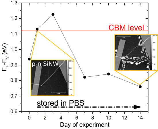
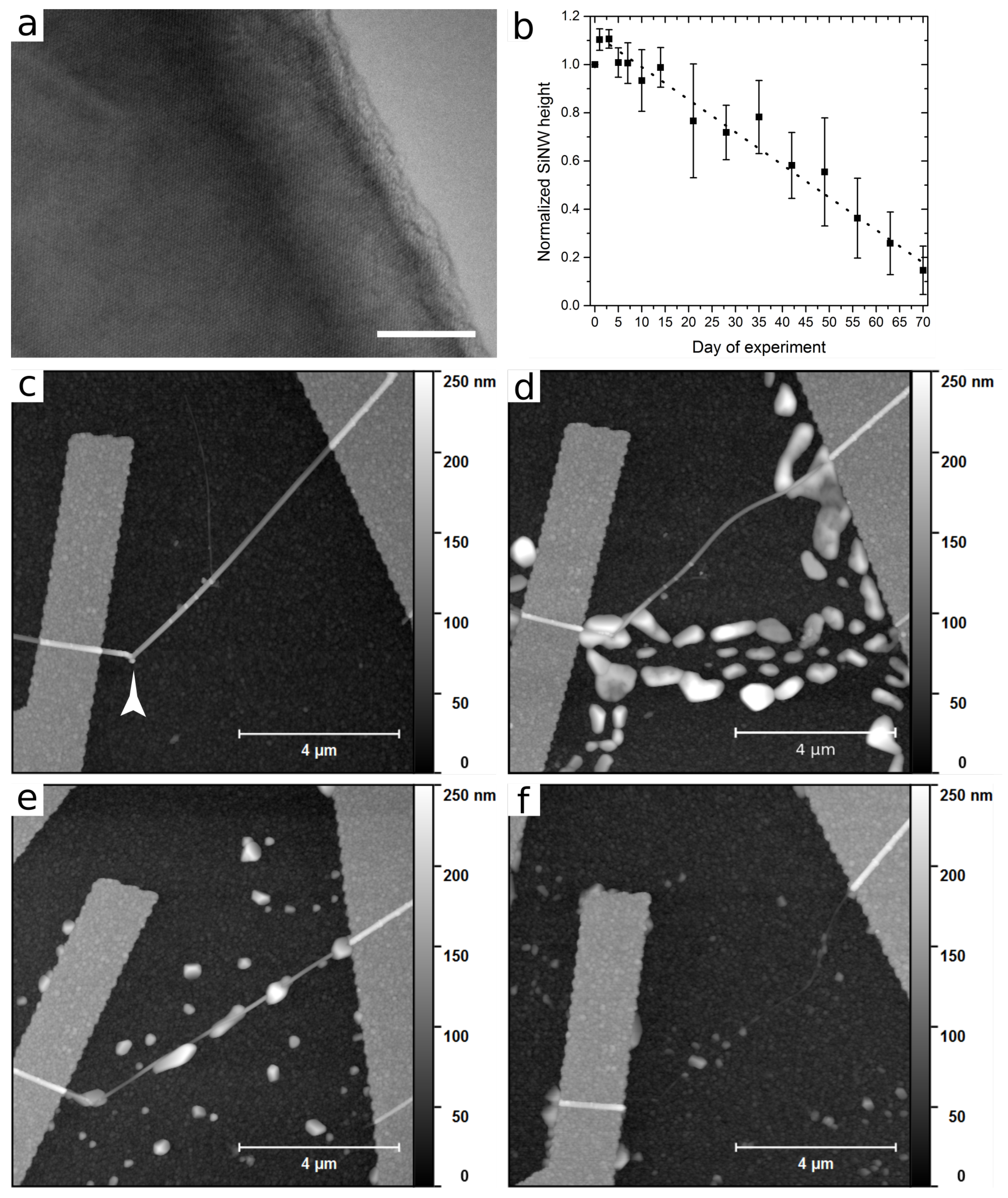
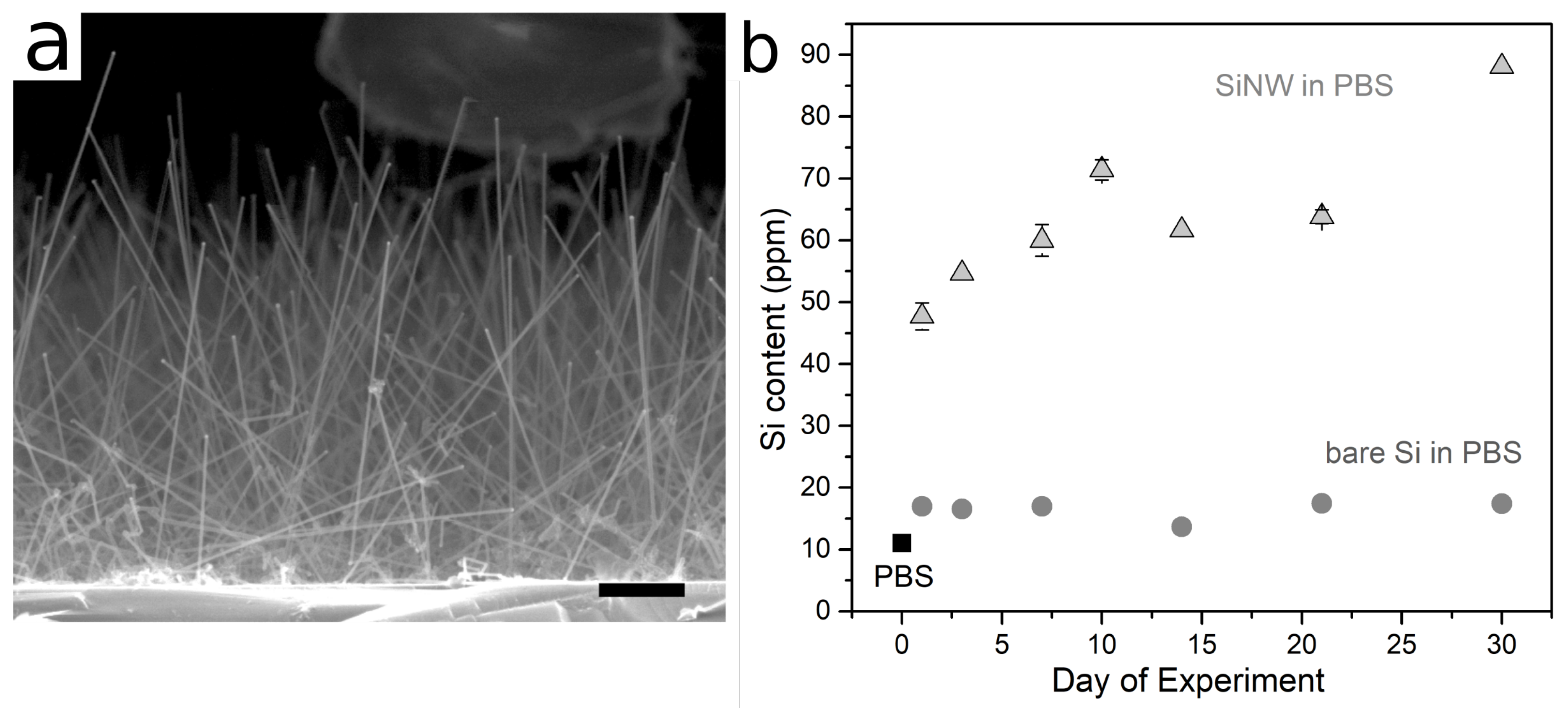
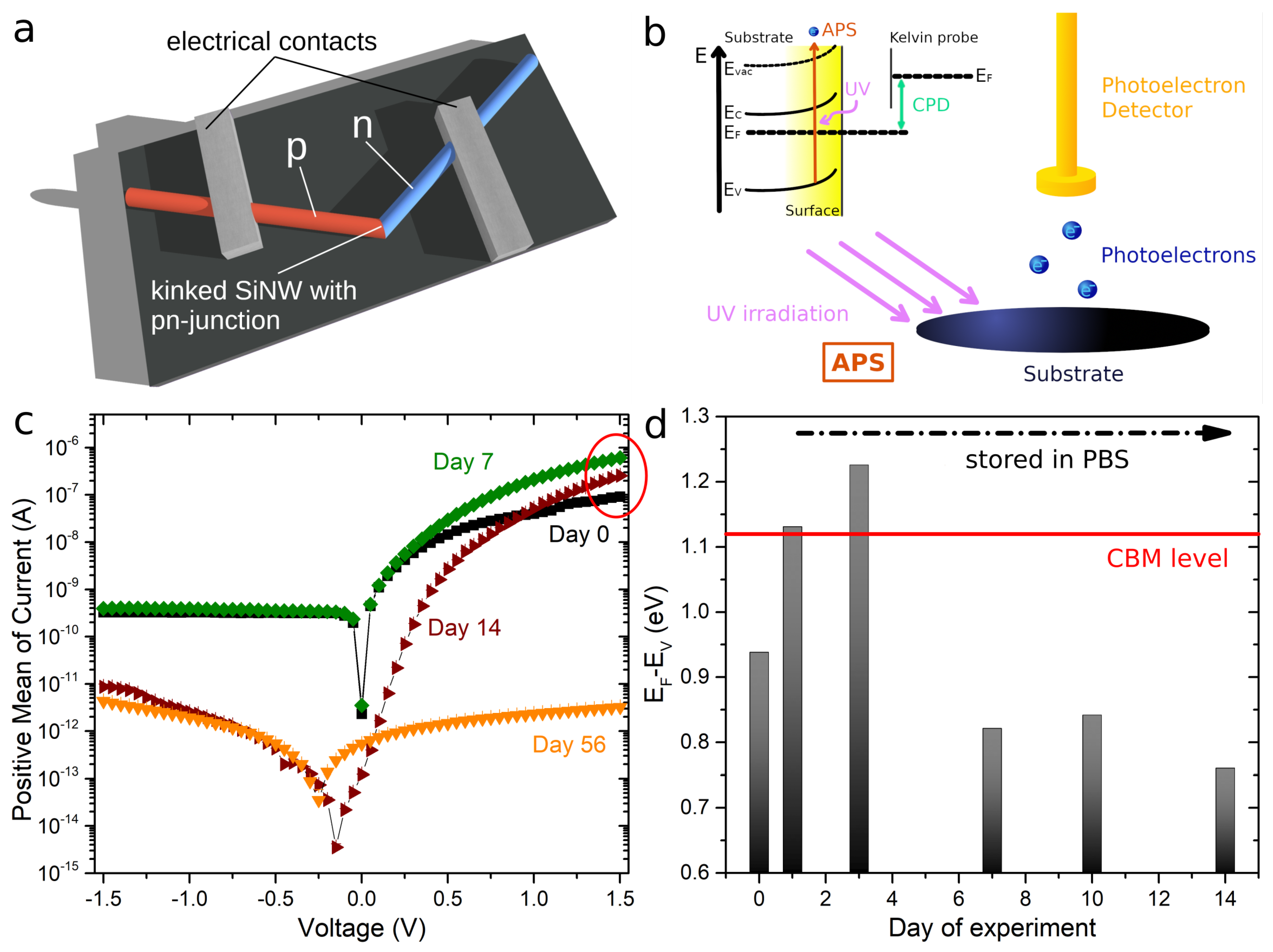
A non-contact and non-destructive ambient Kelvin probe station (KP Technology Ltd., Wick, UK) was used to determine the SiNW work function from the contact potential difference (CPD) between a vibrating gold tip and the SiNWs growth substrate, as recently demonstrated [18]. Prior to each measurement, the work function of the gold coated tip was calibrated using a standard gold substrate and ambient photoelectron spectroscopy with absolute energy calibration. For each SiNW sample, two CPD measurements were carried out at different positions of the respective substrate. Thus, each CPD or APS measurement represents an average measurement across a considerable number of nanowires (ca. 5 × 10 9 nanowires per measurement at an estimated density of ca. 175 nanowires/ μ m 2 ). The method therefore has the advantage of complementing the single nanowire measurements in diminishing the influence of nanowire-to-nanowire variations. Wavelengths ranging from 180 nm to 320 nm were applied for the APS measurements. Based on the theory of photoemission for metals and semiconductors, the absolute surface position of the Fermi level and the valence band edge could be determined, respectively [19]. All data were plotted and fitted using Origin 9.0 software, (Additive, Friedrichsdorf, Germany).

3. Results

It has been shown that Si nanomaterials are not stable in an aqueous environment [11,20]. We verified the assumption that the dissolution reaction at the surface of silicon oxide will become more pronounced with a higher surface to volume ratio by measuring the Si release into the surrounding solution using inductively coupled plasma atomic emission spectroscopy (ICP-AES; Figure 1b). This elemental analysis revealed that a bulk Si surface covered with silicon oxide released a small amount of Si into the surrounding solution. However, when the surface area was increased by decorating the bare silicon surface with SiNWs (Figure 1a), all of which were covered with native oxide of roughly 1.5 nm in thickness [21] (see Figure 2a), the release of Si drastically increased by up to 4.5 folds in the surrounding PBS (Figure 1b, gray triangles compared to dark gray dots).
This preliminary experiment supported the notion that SiNWs degraded in a (simulated) physiological environment by a dissolution reaction at their oxide surface. To characterize the dissolution rate quantitatively and elucidate the relevant changes in SiNWs for biochemical sensor applications, we monitored the diameter of single SiNWs employing atomic force microscopy (AFM). We took the height of a SiNW as a representative measure for the diameter, as the height would be least affected by artifacts emerging from the scanning tip geometry compared to lateral measurements. Phosphate buffered saline (PBS) and a temperature of 37 ° C were chosen to simulate typical physiological test conditions.
Transmission electron microscopy (TEM) analysis (Figure 2a) revealed the morphology of the SiNWs before immersion in PBS. The images confirm the single-crystalline structure of the SiNW and the presence of a thin (ca. 2 nm thick) amorphous layer around the nanowire, most likely corresponding to the native oxide layer [21].
The AFM measurements (Figure 2c–f) showed that it took about 10 weeks until SiNWs with an initial diameter of 75–95 nm were no longer discernible from the surrounding substrate roughness. The height values extracted from the AFM analysis are shown in in Figure 2b. To consider the varying initial diameters of individual SiNWs, the measured height was individually normalized to the respective Day 0 value. Whereas initially the diminutive changes in SiNW height were not discernible at the large variation of height values measured (see Figure S1 in the supporting information), the cumulative changes became apparent after around two weeks.
The variation between the measured values was high even for values measured on a single SiNW. This was partly due to the intrinsic variation of the material and the measurement method but might also be attributed to the SiNWs bending upwards away from the substrate surface instead of lying flat. The clearly visible temporary side bending of the SiNW in Figure 2c–f may serve as an indication for this assumption. Due to our use of height values as a measure for the diameter, the diameter in the present data might have been overestimated. However, as this is a systematic error, a dissolution rate derived from the relative comparison of the different data points should nevertheless represent the true dissolution rate. Such a linear fit of our data yielded a dissolution or etching rate of (1 ± 0.1) nm/day for SiNWs in PBS at 37 ° C.
The most relevant properties of SiNWs in terms of sensing applications are electrical properties. These were monitored in parallel to the AFM measurements using the same SiNWs by recording I-V characteristics at 14 time points between 1 and 70 days of immersion. In the simplest scenario, the conductance of a homogeneously doped SiNW should decrease, if the diameter and consequently the cross-section shrinks due to dissolution. Besides the conductance, the transconductance, commonly utilized as output value for SiNW sensors in FET configuration, should also be affected. However, changes in the leakage current, e.g., due to salt deposition and surface contamination, would also affect the measurements but the measurement of their contribution is non-trivial. To overcome this, we used SiNWs with an encoded p–n junction. As we grew SiNWs in a bottom-up manner, the implementation of p–n junctions was facile and the synthesis did not differ in principle from the one of SiNWs used as FET sensors. To enable localization of the p–n junctions within the SiNWs, we introduced the aforementioned crystal kink at the p–n junction interface (marked with an arrow in Figure 2c) [12]. For a schematic of the measurement set-up, please refer to Figure 3a.
I-V curves are shown in Figure 3c. For improved visibility, only selected but representative curves for a single p–n junction SiNW are depicted (all measured curves for this SiNW can be found in Figure S2). Based on a continuous decrease of the diameter of about 1 nm/day, one would expect in a first assumption to see a decrease of forward current due to an increase of the SiNW resistance. However, on the contrary, we observed an initial increase in forward current after the first days of immersion in PBS. The most pronounced increase by almost one order of magnitude was measured after seven days (circle in Figure 3c, green diamonds compared to black squares of Day 0; see Figure S3 for a plot of relative changes in forward currents).
After this increase in forward current, the expected decrease occurred, which was accordingly also visible in the reverse current. After 56 days, the current at both forward and reverse bias was lower than 10 11 A. At this point, with a symmetric shape of the curve, the typical rectifying diode characteristics of the p–n junction was no longer present and the measured current most likely a result of leakage current.
The counterintuitive behavior in conductivity may be rooted in a change in silicon surface states present at the interface between silicon and its oxide. These surface states lead to the well-known Fermi level pinning, typically in the mid-bandgap region [22], and consequently lead to charge carrier depletion or space charge region formation at the silicon surface. As the initial native oxide layer formed in air is dissolved and rebuilt in an aqueous environment, silicon surface states might be better passivated. This would lower the degree of surface charge carrier depletion and could hence enhance the conductivity despite the diameter decrease [23,24].
To test this hypothesis and examine the electronic surface band structure during dissolution more closely, we performed CPD measurements and APS (Figure 3b). The silicon growth substrate densely covered with n-type SiNWs was measured prior to immersion in PBS at 37 ° C and then repeatedly at different time intervals. With the data obtained in the CPD and APS measurements, the values of the valence band maximum (VBM, corresponding to E V ), surface Fermi level position (E F ) and conduction band minimum (CBM) could be calculated using the common room temperature band gap energy for silicon of 1.12 eV.
Figure 3d shows the difference between the energy levels of the surface valence band edge and the Fermi level (E F -E V ) over immersion, as deduced from the reconstructed electronic surface band structure of n-doped SiNWs when immersed in PBS. Day 0 corresponds to the band structure of n-type SiNW in air. The measurements showed that the Fermi level was shifted towards the conduction band before the immersion. This was in accordance with the high donor doping concentration.
Immersing the SiNWs led to considerable increases in the distance between the valence band edge and Fermi level. The Fermi level intermittently even rose above the CMB level. After seven days of immersion, however, the Fermi level shifted back toward the valence band and stabilized at around 0.8 eV above the valence band, still well above the middle of the band gap expected at 0.56 eV considering the silicon band gap of 1.12 eV.
As recent literature shows, coating SiNW devices with Al 2 O 3 could enhance their lifetime significantly [11]. Therefore, we compared this dissolution rate to the one of SiNWs with a 3.5 nm Al 2 O 3 coating deposited by atomic layer deposition (ALD). Additionally, we tested a submonolayer coating of Al 2 O 3 to verify if a mixed oxide from aluminium and silicon could prevent the dissolution reaction, as suggested by Iler [20]. Again, we measured the SiNW height using AFM (Figure S4). In this experiment, the tested Al 2 O 3 coatings did not have a considerable impact on the longevity of the SiNWs. However, optimizing the ALD deposition might yield improvements, which will be the subject of future studies.

4. Discussion

We confirmed that SiNWs degrade in a simulated physiological environment (PBS) and release Si into the surrounding solution. The degradation of single SiNWs can be monitored by using AFM measurements to estimate the etch rate. We extrapolated that, under the present conditions, SiNWs lose about 1 nm in diameter per day. This rate is well within the range of dissolution rates given for silicon oxide layers that were investigated at different temperatures, including non-physiological ones, demonstrating the temperature dependence of the dissolution process [25,26]. Literature on the dissolution of SiNW under similar conditions [11,27] seem to show comparable dissolution rates, albeit under presumably static conditions, i.e. without a regular exchange of PBS, and with the use of other methods to determine the SiNW diameter.
The SiNW devices were functional for up to seven weeks in PBS at the physiological temperature of 37 ° C. The magnitude of current that was flowing through the device, however, varied by orders of magnitude during degradation. This indicates a variability in conductivity that is detrimental to the reproducibility of silicon nanowire transducer signal interpretation, if SiNWs are used for long-term analytical applications.
Electrical characterization of SiNWs with encoded p–n junctions in parallel with the AFM measurements support the overall diameter decrease. However, the changes in electrical properties do not correlate simply with decreasing diameter. In particular within the first 48 h, immersion in PBS had a drastic effect on the SiNW surface band structure as determined by CPD and APS measurements. During this period, the Fermi level shifted towards the conduction band and was finally situated inside the conduction band itself. This implies a significant accumulation of majority charge carriers, here electrons, at the nanowire surface and thus a significant increase in SiNW conductivity, which is fully supported by the increased forward current of the measured p–n junctions. The exact reason for this Fermi level shift remains to be found, but three aspects are discussed here. First, it is well known that SiO 2 can passivate surface states which are present at the silicon surface, thus reducing charge carrier trapping [28]. The effectiveness of this passivation is directly linked to the oxide quality and the preparation method. The hydrolytic dissolution of the SiNWs is accompanied by the dissolution of the native oxide, followed by a re-oxidation of the silicon [10]. Considering the estimated etch rate, it is reasonable to assume that the initial native oxide grown in air is exchanged within the first 48 h by an oxide grown in the liquid. Thus, with the re-arrangement of the oxide layer, the passivation of surface states may change. A second aspect that can be discussed is the evolution of a fixed positive interface charge in SiO 2 [22,28] that would lead to an electron accumulation as observed. The oxide-recovering oxidation reaction may be the source of such a charge imbalance and may lead to the observed increased Fermi level [29]. The third point is the PBS electrolyte itself and the ions that should in principle balance the overall charge situation. The electrolyte, however, potentially also affects the formation of surface states. Alkali metal cations can replace hydrogen on the silanol hydroxyl groups and the deposition of cations such as sodium and potassium may lead to a strong accumulation of electrons at the surface. As a side effect, this replacement can promote an increasing bond angle and therefore facilitate the access of water molecules to the surface, which in turn increase the dissolution rate [30]. However, further studies are required to determine the origin for the observed initial change in surface band structure to fully explain the observed behavior including the significant shift of the Fermi level well above the conduction band edge.
After a week of immersion, the band structure seemed to stabilize. This corresponds well with the steady decrease in forward current observed in the I-V measurements. From this point on, the electrical properties seem to be dominated by the anticipated increase in resistance due to the reduction in SiNW diameter.
Next to the SiNW dissolution, electrical contact degradation is a critical issue for the electronic properties of the device that could affect the measured total resistance of the system. Pinholes in the metal contact for example could lead to an increased contact resistance due to PBS entering the metal–semiconductor interface and diminishing the electrical contact. However, failure of the metal–semiconductor interface is expected to cause an abrupt resistance change rather than a slow change that is well aligned with the SiNW dissolution and with changes in the SiNW surface band structure, as in the present case. We could neither observe any pinholes in our contact metalization nor any delamination due to total or partial adhesion loss using SEM and AFM. Therefore, the measured electrical behavior was probably governed by the p–n junction in the kinked SiNW rather than by the electrical ohmic contacts.
The observed drastic changes in surface band structure and resulting electronic properties reveal that SiNW instability not only has consequences for their durability but also reliability and reproducibility in sensor applications. These changes already occurred in one of the simpler systems to simulate physiological conditions, namely PBS. Conditions in vitro and considerably more so in vivo present themselves as more complex. The proteins that additionally are present under these conditions potentially influence the dissolution process as well as the surface potential of nanosensors, increasing the involved parameters. Future experiments will have to deconvolute the influence of these components on the properties of nanosensors.
However, even if SiNWs turn out to be less applicable for long-term sensor applications in physiological conditions, they may still be used as readily integrated, highly efficient and label-free sensors in lab-on-chip systems [31], where one-time usage may eventually even be highly desired, e.g., in trace-analytic applications and therapeutic point-of-care diagnostics. The dissolution of SiNWs as electronic building blocks by releasing non-toxic products might also be beneficial with a view to the emerging field of green and disposable electronics [32,33]. Additionally, short-term in vitro applications as highly sensitive and localized sensors have the potential to progress medical research by providing nano-sized analytical tools [34,35,36,37].

5. Conclusions

We have shown that SiNWs dissolve under simulated physiological conditions and exhibit unexpected changes in electrical properties during this process. The absolute reconstruction of the surface band structure using CPD measurements and APS demonstrated considerable changes in the underlying surface band structure that are in accordance with the observed conductivity changes. However, the exact role of the interactions of the SiNWs with the surrounding ionic solutions in causing the drastic changes in surface band structure remains to be examined in future studies. A more profound knowledge about these processes may eventually lead to reliable biomedical nanosensors that combine the high sensitivity of nanoscale devices with increased robustness.

Supplementary Materials

The following are available online at https://www.mdpi.com/2076-3417/9/4/804/s1, Figure S1: Absolute values of AFM height measurements, Figure S2: Complete series of I–V measurements of a p–n junction, Figure S3: Relative change of forward and reverse currents over time, Figure S4: Al 2 O 3 coatings and their dissolution.

Author Contributions

Conceptualization, A.M.S. and S.S.; Validation, all authors; Formal Analysis, A.M.S., T.S., M.N. and X.H.; Investigation, A.M.S., T.S., M.N., X.H., R.S., D.G. and A.M.; Writing—Original Draft Preparation, A.M.S.; Writing—Review and Editing, all authors; Visualization, A.M.S. and T.S.; Supervision, S.S.; Project Administration, S.S.; and Funding Acquisition, S.S.

Funding

This research was funded by the Bundesministerium für Bildung und Forschung (BMBF), Germany, grant number NanoMatFutur: FKZ 13N12545 and the Deutsche Forschungsgemeinschaft (DFG), Germany, grant number STE 2545-1/1.

Acknowledgments

The authors would like to thank S. Jenisch and P. Muralidhar, Institute of Electron Devices and Circuits, Ulm University, and F. Huber and K. Thonke, Institute of Quantum Matter, Ulm University, for experimental support, and M. Lang and B. Mizaikoff, Service Center Elementanalytik, Ulm University, for ICP-AES measurements. The authors further would like to thank M.N. Holme, Karolinska Institutet, for critically proofreading the manuscript.

Conflicts of Interest

The authors declare no conflict of interest.

Abbreviations

The following abbreviations are used in this manuscript:
AFMatomic force microscopy
ALDatomic layer deposition
APSambient pressure photoemission spectroscopy
AuNPgold nanoparticle
CBMconduction band minimum
CMOScomplementary metal-oxide-semiconductor
CPDcontact potential difference
CVDchemical vapor deposition
E F Fermi level
E V valence band energy level
FETfield-effect transistor
ICP-AESinductively coupled plasma atomic emission spectroscopy
PBSphosphate buffered saline
SEMscanning electron microscopy
SiNWsilicon nanowire
TEMtransmission electron microscopy
TMAtrimethyl aluminium
VBMvalence band maximum
VLSvapor–liquid–solid

References

  1. Cui, Y.; Wei, Q.; Park, H.; Lieber, C.M. Nanowire Nanosensors for Highly Sensitive and Selective Detection of Biological and Chemical Species. Science 2001, 293, 1289–1292. [Google Scholar] [CrossRef] [PubMed]
  2. Chen, K.I.; Li, B.R.; Chen, Y.T. Silicon nanowire field-effect transistor-based biosensors for biomedical diagnosis and cellular recording investigation. Nano Today 2011, 6, 131–154. [Google Scholar] [CrossRef]
  3. Hahm, J.I.; Lieber, C.M. Direct Ultrasensitive Electrical Detection of DNA and DNA Sequence Variations Using Nanowire Nanosensors. Nano Lett. 2004, 4, 51–54. [Google Scholar] [CrossRef]
  4. Zhang, G.J.; Zhang, L.; Huang, M.J.; Luo, Z.H.H.; Tay, G.K.I.; Lim, E.J.A.; Kang, T.G.; Chen, Y. Silicon nanowire biosensor for highly sensitive and rapid detection of Dengue virus. Sens. Actuators B Chem. 2010, 146, 138–144. [Google Scholar] [CrossRef]
  5. Wu, J. Semiconducting silicon nanowire array fabrication for high throughput screening in the biosciences. In Semiconducting Silicon Nanowires for Biomedical Applications; Coffer, J.L., Ed.; Woodhead Publishing: Sawston, UK, 2014; Chapter 9; pp. 171–191. [Google Scholar]
  6. Luo, L.; Jie, J.; Zhang, W.; He, Z.; Wang, J.; Yuan, G.; Zhang, W.; Wu, L.C.M.; Lee, S.T. Silicon nanowire sensors for Hg2+ and Cd2+ ions. Appl. Phys. Lett. 2009, 94, 193101. [Google Scholar] [CrossRef]
  7. Elfström, N.; Juhasz, R.; Sychugov, I.; Engfeldt, T.; Karlström, A.E.; Linnros, J. Surface Charge Sensitivity of Silicon Nanowires: Size Dependence. Nano Lett. 2007, 7, 2608–2612. [Google Scholar] [CrossRef] [PubMed]
  8. Lis, D.; Backus, E.H.G.; Hunger, J.; Parekh, S.H.; Bonn, M. Liquid flow along a solid surface reversibly alters interfacial chemistry. Science 2014, 344, 1138–1142. [Google Scholar] [CrossRef] [PubMed]
  9. Iler, R. The Chemistry of Silica—Solubility, Polymerization, Colloid and Surface Properties, and Biochemistry; Wiley-Interscience: Hoboken, NJ, USA, 1979. [Google Scholar]
  10. Morita, M.; Ohmi, T.; Hasegawa, E.; Kawakami, M.; Ohwada, M. Growth of native oxide on a silicon surface. J. Appl. Phys. 1990, 68, 1272–1281. [Google Scholar] [CrossRef]
  11. Zhou, W.; Dai, X.; Fu, T.M.; Xie, C.; Liu, J.; Lieber, C.M. Long Term Stability of Nanowire Nanoelectronics in Physiological Environments. Nano Lett. 2014, 14, 1614–1619. [Google Scholar] [CrossRef] [PubMed] [Green Version]
  12. Xu, L.; Jiang, Z.; Qing, Q.; Mai, L.; Zhang, Q.; Lieber, C.M. Design and Synthesis of Diverse Functional Kinked Nanowire Structures for Nanoelectronic Bioprobes. Nano Lett. 2013, 13, 746–751. [Google Scholar] [CrossRef] [PubMed] [Green Version]
  13. Wagner, R.S.; Ellis, W.C. Vapor-liquid-solid mechanism of single crystal growth. Appl. Phys. Lett. 1964, 4, 89–90. [Google Scholar] [CrossRef]
  14. Cui, Y.; Lauhon, L.J.; Gudiksen, M.S.; Wang, J.; Lieber, C.M. Diameter-controlled synthesis of single-crystal silicon nanowires. Appl. Phys. Lett. 2001, 78, 2214–2216. [Google Scholar] [CrossRef]
  15. Wu, Y.; Cui, Y.; Huynh, L.; Barrelet, C.J.; Bell, D.C.; Lieber, C.M. Controlled Growth and Structures of Molecular-Scale Silicon Nanowires. Nano Lett. 2004, 4, 433–436. [Google Scholar] [CrossRef]
  16. Steinbach, A.M.; Sandner, T.; Mizaikoff, B.; Strehle, S. Gas phase silanization for silicon nanowire sensors and other lab-on-a-chip systems. Phys. Status Solidi C 2015, 13, 135–141. [Google Scholar] [CrossRef]
  17. Nečas, D.; Klapetek, P. Gwyddion: An open-source software for SPM data analysis. Cent. Eur. J. Phys. 2012, 10, 181–188. [Google Scholar] [CrossRef]
  18. Challinger, S.; Baikie, I.; Birdwell, A.G.; Strehle, S. Construction of the Energy Band Diagram of Hydrogen Terminated Diamond and Silicon Nanowires. Phys. Status Solidi C 2017, 14, 1700152. [Google Scholar]
  19. Baikie, I.D.; Grain, A.C.; Sutherland, J.; Law, J. Ambient pressure photoemission spectroscopy of metal surfaces. Appl. Surf. Sci. 2014, 323, 45–53. [Google Scholar] [CrossRef] [Green Version]
  20. Iler, R.K. The Occurrence, Dissolution, and Deposition of Silica. In The Chemistry of Silica—Solubility, Polymerization, Colloid and Surface Properties, and Biochemistry; Wiley-Interscience: Hoboken, NJ, USA, 1979; Chapter 1; pp. 3–115. [Google Scholar]
  21. Philipp, H.; Taft, E. An optical characterization of native oxides and thin thermal oxides on silicon. J. Appl. Phys. 1982, 53, 5224–5229. [Google Scholar] [CrossRef]
  22. Mizsei, J. Fermi-level pinning and passivation on the oxide-covered and bare silicon surfaces and interfaces. Vacuum 2002, 67, 59–67. [Google Scholar] [CrossRef]
  23. Helms, C.R.; Poindexter, E.H. The silicon-silicon dioxide system: Its microstructure and imperfections. Rep. Prog. Phys. 1994, 57, 791. [Google Scholar] [CrossRef]
  24. Schmidt, V.; Senz, S.; Gösele, U. Influence of the Si/SiO2 interface on the charge carrier density of Si nanowires. Appl. Phys. A 2007, 86, 187–191. [Google Scholar] [CrossRef]
  25. Kang, S.; Hwang, S.; Cheng, H.; Yu, S.; Kim, B.H.; Kim, J.; Huang, Y.; Rogers, J.A. Dissolution Behaviors and Applications of Silicon Oxides and Nitrides in Transient Electronics. Adv. Funct. Mater. 2014, 24, 4427–4434. [Google Scholar] [CrossRef]
  26. Fang, H.; Zhao, J.; Yu, K.J.; Song, E.; Farimani, A.B.; Chiang, C.H.; Jin, X.; Xue, Y.; Xu, D.; Du, W.; et al. Ultrathin, transferred layers of thermally grown silicon dioxide as biofluid barriers for biointegrated flexible electronic systems. Proc. Natl. Acad. Sci. USA 2016, 113, 11682–11687. [Google Scholar] [CrossRef] [PubMed] [Green Version]
  27. Peled, A.; Pevzner, A.; Peretz Soroka, H.; Patolsky, F. Morphological and chemical stability of silicon nanostructures and their molecular overlayers under physiological conditions: Towards long-term implantable nanoelectronic biosensors. J. Nanobiotechnol. 2014, 12, 7. [Google Scholar] [CrossRef] [PubMed]
  28. Glunz, S.W.; Biro, D.; Rein, S.; Warta, W. Field-effect passivation of the SiO2Si interface. J. Appl. Phys. 1999, 86, 683–691. [Google Scholar] [CrossRef]
  29. Velusamy, T.; Mitra, S.; Macias-Montero, M.; Svrcek, V.; Mariotti, D. Varying Surface Chemistries for p-Doped and n-Doped Silicon Nanocrystals and Impact on Photovoltaic Devices. ACS Appl. Mater. Interfaces 2015, 7, 28207–28214. [Google Scholar] [CrossRef] [PubMed]
  30. Lee, Y.K.; Yu, K.J.; Kim, Y.; Yoon, Y.; Xie, Z.; Song, E.; Luan, H.; Feng, X.; Huang, Y.; Rogers, J.A. Kinetics and Chemistry of Hydrolysis of Ultrathin, Thermally Grown Layers of Silicon Oxide as Biofluid Barriers in Flexible Electronic Systems. ACS Appl. Mater. Interfaces 2017, 9, 42633–42638. [Google Scholar] [CrossRef] [PubMed]
  31. Zhang, G.J.; Ning, Y. Silicon nanowire biosensor and its applications in disease diagnostics: A review. Anal. Chim. Acta 2012, 749, 1–15. [Google Scholar] [CrossRef] [PubMed]
  32. Kang, S.K.; Koo, J.; Lee, Y.K.; Rogers, J.A. Advanced Materials and Devices for Bioresorbable Electronics. Acc. Chem. Res. 2018, 51, 988–998. [Google Scholar] [CrossRef] [PubMed]
  33. Hwang, S.W.; Tao, H.; Kim, D.H.; Cheng, H.; Song, J.K.; Rill, E.; Brenckle, M.A.; Panilaitis, B.; Won, S.M.; Kim, Y.S.; et al. A Physically Transient Form of Silicon Electronics. Science 2012, 337, 1640–1644. [Google Scholar] [CrossRef] [PubMed] [Green Version]
  34. Cohen-Karni, T.; Casanova, D.; Cahoon, J.F.; Qing, Q.; Bell, D.C.; Lieber, C.M. Synthetically Encoded Ultrashort-Channel Nanowire Transistors for Fast, Pointlike Cellular Signal Detection. Nano Lett. 2012, 12, 2639–2644. [Google Scholar] [CrossRef] [PubMed] [Green Version]
  35. Tian, B.; Cohen-Karni, T.; Qing, Q.; Duan, X.; Xie, P.; Lieber, C.M. Three-Dimensional, Flexible Nanoscale Field-Effect Transistors as Localized Bioprobes. Science 2010, 329, 830–834. [Google Scholar] [CrossRef] [PubMed] [Green Version]
  36. Qing, Q.; Jiang, Z.; Xu, L.; Gao, R.; Mai, L.; Lieber, C.M. Free-standing kinked nanowire transistor probes for targeted intracellular recording in three dimensions. Nat. Nanotechnol. 2013, 9, 142–147. [Google Scholar] [CrossRef] [PubMed] [Green Version]
  37. Gao, R.; Strehle, S.; Tian, B.; Cohen-Karni, T.; Xie, P.; Duan, X.; Qing, Q.; Lieber, C.M. Outside Looking In: Nanotube Transistor Intracellular Sensors. Nano Lett. 2012, 12, 3329–3333. [Google Scholar] [CrossRef] [PubMed] [Green Version]
Figure 1. (a) SEM image of SiNW densely grown onto a Si wafer piece. Scale bar 1 μ m. (b) Si release from a sample covered densely with SiNW (triangles) to the surrounding PBS in the course of immersion at a temperature of at 37 ° C as measured with ICP-AES, compared to a bare silicon wafer piece serving as control (dots). For comparison, the Si content of PBS alone is plotted at Day 0 (square).
Applsci 09 00804 g001
Figure 2. (a) TEM analysis of a SiNW covered with a native oxide layer prior to immersion in PBS. Scale bar 10 nm. (b) Decrease of SiNW height (corresponding to the diameter) as measured with AFM over time during immersion in PBS at 37 ° C. The error bars denote the standard deviation and the dotted line represents a linear fit of the data. (cf) Height scans of a single SiNW after immersion in PBS at 37 ° C for: 3 days (c); 14 days (d); 35 days (e); and 63 days (f) as measured with AFM. The p–n junction encoded as a kink is marked with an arrow in sub-figure (c).
Applsci 09 00804 g002
Figure 3. (a) Schematic of the I-V measurement set-up with the kinked SiNW in red (p-type branch) and blue (n-type branch) integrated on a chip (black) as a p–n junction. (b) Schematic of the working principle of the surface band structure (upper left, pale yellow area) reconstruction. Using CPD measurements and APS, it is possible to determine the surface Fermi level and the ionization potential. With these two values and the knowledge of the material’s band gap energy, the surface band structure can be reconstructed. The APS method uses UV irradiation (violet) to liberate photoelectrons (blue) from the material, which are then registered by the detector (gold). (c) Decay of the electrical properties of a single SiNW p–n junction plotted as I-V curves on a logarithmic scale. For better legibility, only selected time points are shown. The circle highlights the increase in forward current during the first days of immersion. The complete measurement series is shown in Figure S2. (d) Time dependent changes in electronic surface band structure of n-type SiNWs during immersion in PBS at 37 ° C. For comparison the conduction band minimum (CBM) for the common band gap energy of Si of 1.12 eV is given as a red line.
Applsci 09 00804 g003

