Article

Numerical Study on the Absorption Characteristics of Subwavelength Metallic Gratings Covered with a Lossy Dielectric Layer

Reality Display Device Research Group, Electronics and Telecommunications Research Institute, Daejeon 34129, Korea
*
Authors to whom correspondence should be addressed.
Appl. Sci. 2018, 8(9), 1445; https://doi.org/10.3390/app8091445
Submission received: 14 July 2018 / Revised: 14 August 2018 / Accepted: 22 August 2018 / Published: 24 August 2018
(This article belongs to the Special Issue Photonic Metamaterials)

Abstract

:
Optical absorbers have been a topic of intense research due to their importance in many applications. In particular, multi-band and perfect absorption features in a desired frequency range are essential in broadband applications. In this work, we numerically studied the absorption properties of subwavelength metallic gratings coated with a dielectric layer. Here, the structure is considered to be an integration between a resonant cavity and a subwavelength metallic grating. Two appropriately designed structures can exhibit multi-band absorption properties. In addition to the numerical simulation results, we elaborate on determining the appropriate structural parameters that yield the desired spectral absorption profile in the visible range. We also numerically identify critical coupling conditions for perfect absorption.

Graphical Abstract

1. Introduction

Optical absorbers are an essential optical component that can be fabricated by using various materials and structures [1,2,3,4,5]. Absorbing structures have been used in a number of diverse applications, including solar-energy harvesting [6,7,8,9,10], light modulation [11,12,13,14,15], and optical sensing and detection [16,17,18,19]. There are several principles and methods used to fabricate electromagnetic wave absorbers, such as stacked metal-dielectric-metal (MIM) structures [20,21,22,23], metamaterials and metasurfaces [1,2,3,4,10,24,25,26,27,28,29,30], asymmetric Fabry–Pérot (FP) cavities with ultrathin high-absorption dielectric layers [12,31,32], and subwavelength metallic gratings [1,9,14,15,17,18,33,34,35,36,37].
Among them, reflection-type subwavelength metallic gratings have been widely adopted due to their relatively simple geometry and practical applicability. It is interesting that visible light can be strongly confined in deep-subwavelength scale grating grooves with width and depth of a few nanometers [34]. Incident waves are absorbed due to coupling in the metallic grating as a gap surface plasmon (GSP) mode [1,18,33,34,35,36,37,38,39,40,41,42,43,44,45]. Light is subsequently trapped within the grating cavity, thereby being absorbed due to metallic Ohmic loss. These types of structures have advantages in that they are capable of perfect absorption, and they are robust in terms of their angular dependence. For these reasons, many studies have focused on effective use of these structures in specific frequency ranges. In addition to absorber applications, it was recently shown that reflection-type spatial light modulation can be implemented by using appropriately designed subwavelength gratings and tunable materials [14,15].
In this paper, we numerically studied the absorption properties of a subwavelength metallic grating coated with a lossy dielectric layer. The roles of the grating and coated dielectric in overall absorbance are analyzed by regarding the subwavelength grating as a homogeneous semi-infinite effective medium. Moreover, we show that subwavelength grating reflectors can be used to create critically coupled perfect absorption conditions. Although these kinds of grating-related structures have been actively studied, detailed numerical studies on the absorption characteristics of lossy dielectric coated subwavelength metallic gratings have not been reported to the best of our knowledge. The presented results can provide a useful platform for understanding and designing structures that include reflective subwavelength gratings.

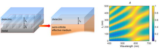
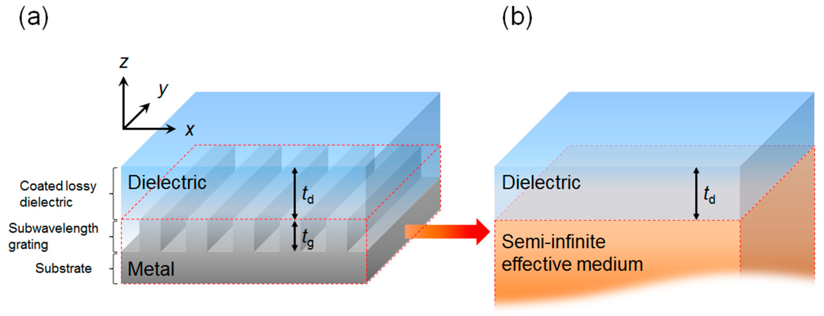
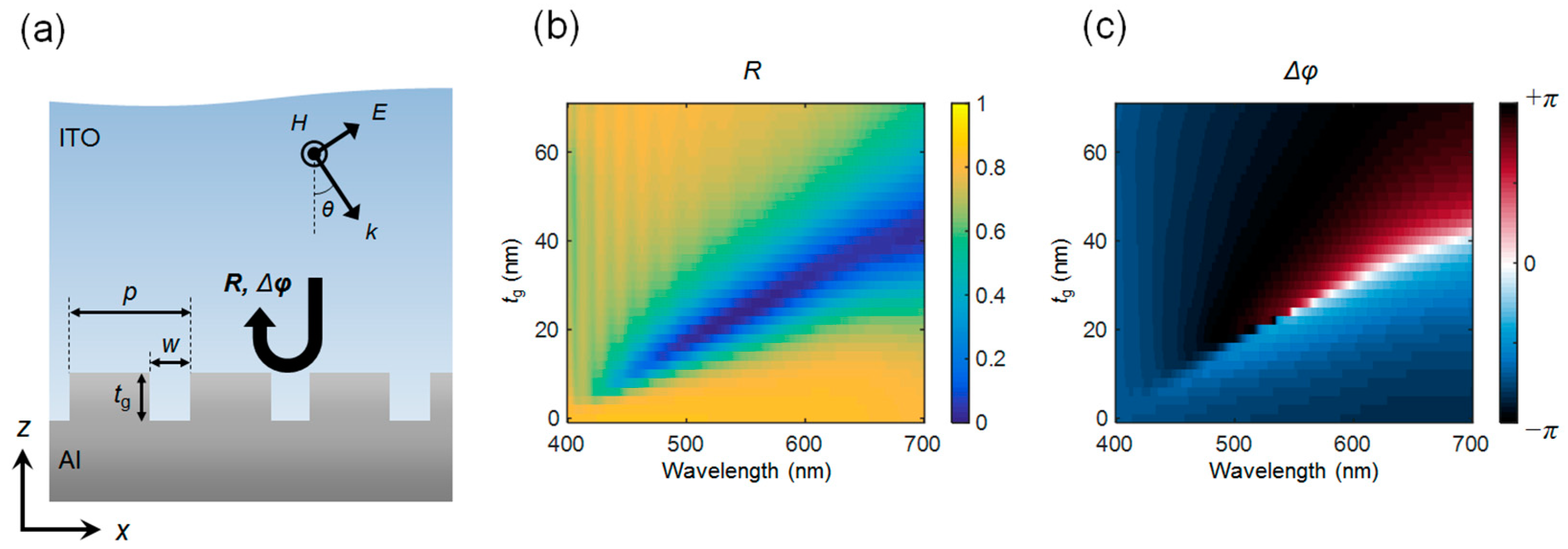
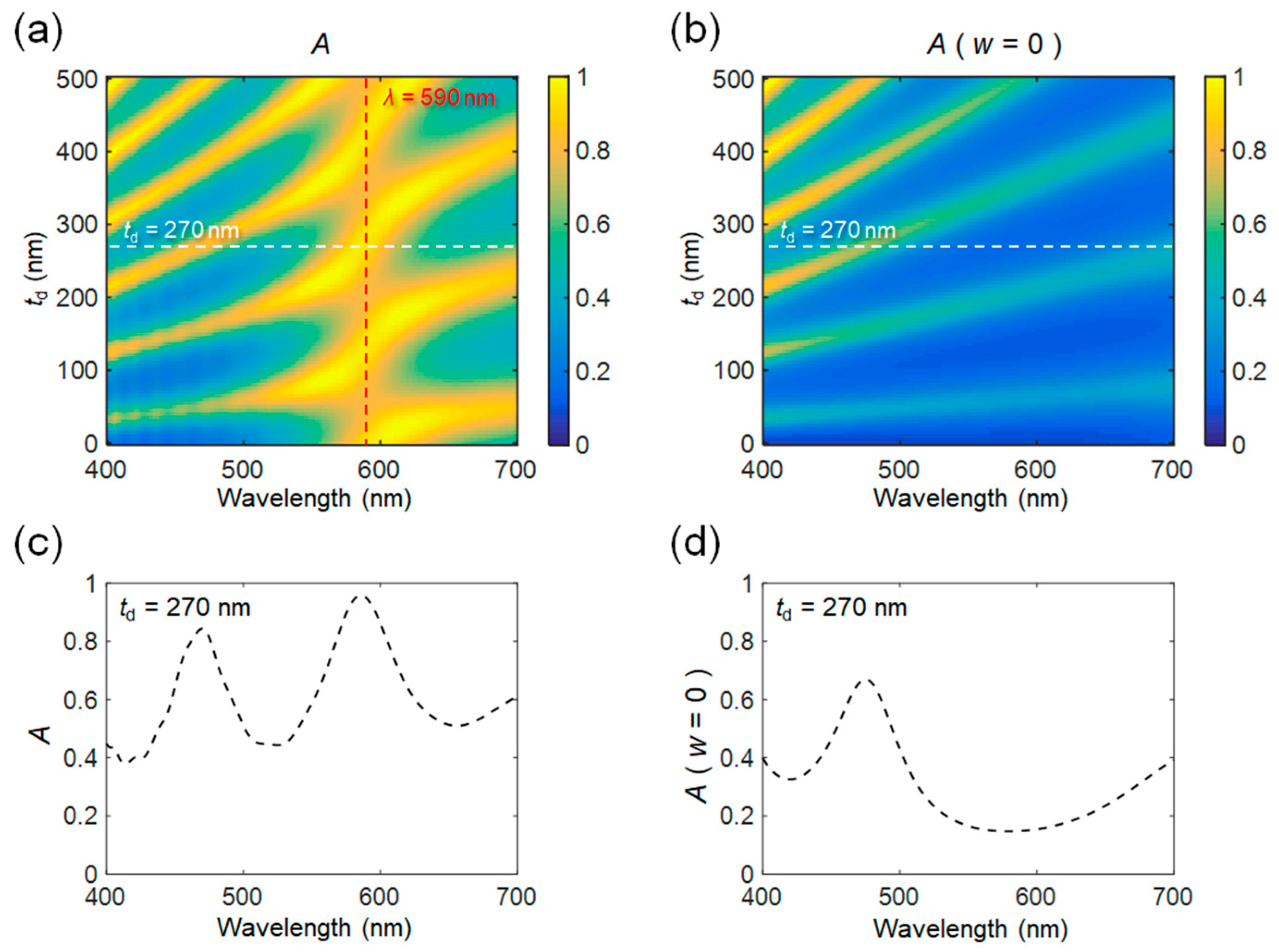
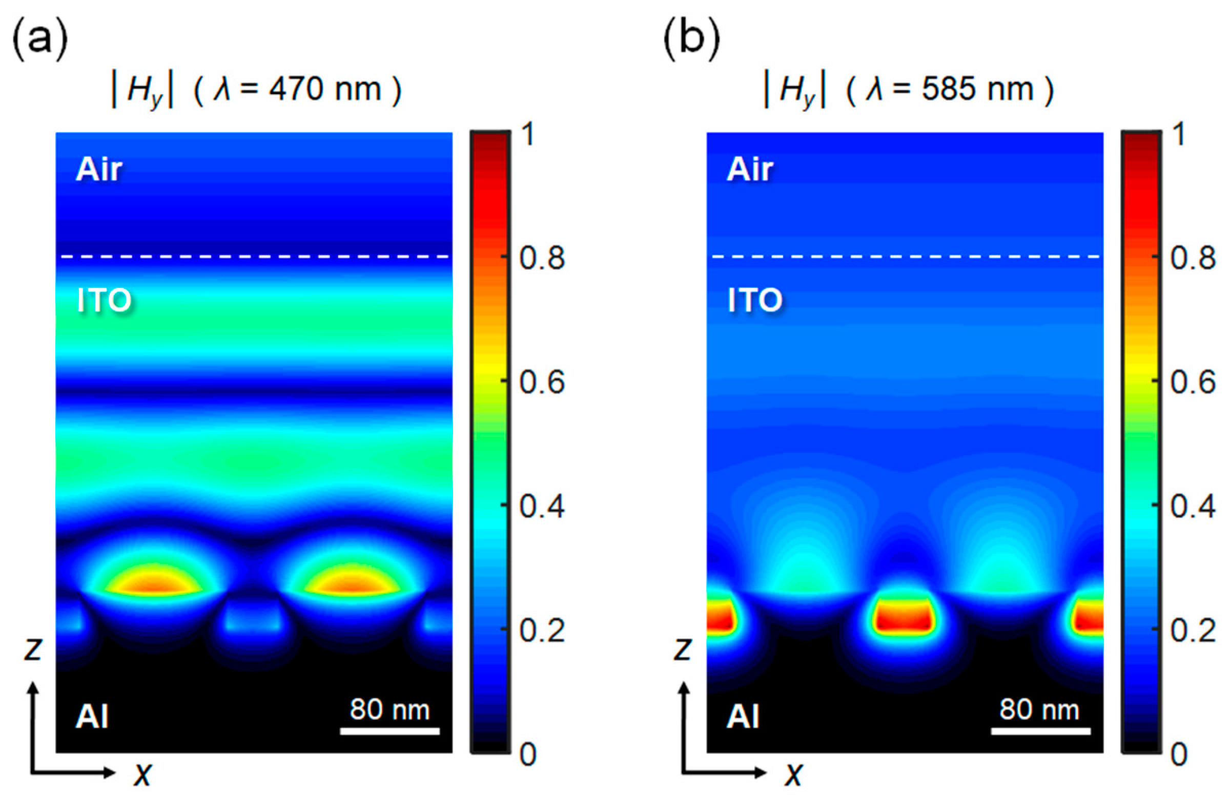
2. Absorption Characteristics of a Subwavelength Metallic Grating Covered with a Lossy Dielectric Layer

A subwavelength metallic grating covered with a dielectric layer is illustrated in Figure 1a. This structure contains stacked dielectric resonant cavity, metallic subwavelength grating, and metal substrate layers. Since the subwavelength grating reflects light without generating higher-order diffraction peaks, the grating and substrate can be equivalently replaced by a semi-infinite effective medium substrate, as shown in Figure 1b. In this model, which is an asymmetric FP resonant cavity, the reflection coefficient between the dielectric resonant cavity and effective medium substrate can be obtained by numerically calculating the modulated amplitude and phase profiles created by the grating. We note that the magnitude of the reflection coefficient is associated with absorption due to localized GSP modes within the grating cavities.
Calculation of the reflection coefficient for the semi-infinite effective medium can be implemented with the model shown in Figure 2a. The one-dimensional grating in this model is periodic along the x-axis and is embedded in a background dielectric medium. The period and thickness of the grating are labelled p and tg, respectively, and w is the width of the grating cavity. Aluminum (Al) and indium tin oxide (ITO) are used as the metal and lossy dielectric, respectively. We note that lossy dielectric materials other than ITO are also applicable, which may result in more desirable absorption. The metal substrate is 100 nm thick, thus we can assume there is no transmission of visible light. Transverse magnetic (TM) plane waves are incident with angle θ. Here, we only consider TM polarized incident plane waves since this is necessary to generate GSP modes in the grating cavity at normal incidence (θ = 0).
Due to the polarization selectivity of plasmonic resonance [46], one-dimensional plasmonic gratings have unique applications, such as controlled thermal emitters and polarimetric detectors [47,48,49,50]. To implement polarization-insensitivity, the structure should be extended to two-dimensional configurations with four-fold rotational symmetry [18,37]. This is because both TM and TE (transverse electric) polarized light can be coupled to GSP modes in grating cavities arranged along two orthogonal directions. Polarization insensitivity based on geometric symmetry can be found in other types of two-dimensional plasmonic structures, e.g., in patterned MIM absorbers [20,21].
The simulated spectral reflectance and phase shift maps are shown in Figure 2b,c, where the effect of the upper ITO layer is not considered. The optical response of the grating is calculated using the transfer matrix method (TMM) [51]. In order to reduce the number of design variables, we set the pitch and width of the grating to p = 160 nm and w = 40 nm throughout this work, respectively. Although we only investigated the effect of grating thickness, it is notable that the resonance condition in reflective gratings is also closely related to its period and width, as can be found in relevant previous studies [14,18,37]. As shown in Figure 2b, reflection dips in the visible spectrum can be tuned by selecting the proper grating thickness. Since we can ignore the transmitted components, these reflection dips directly correspond to absorption peaks. Thus, the grating thickness can be chosen in accordance with an absorption band of interest. It is expected that these absorption properties will be maintained when the grating is coated with an ITO layer with finite thickness.
Absorption in the Al grating coated with ITO of finite thickness can be calculated using the reflection results at the interface between the Al grating and ITO. Figure 3a shows the reflection and transmission coefficients at two interfaces of the structure in which the grating and substrate layers are equivalently replaced by the semi-infinite effective medium. Here, we take tg = 30 nm, and the corresponding magnitude and phase profiles of the reflection coefficient from ITO to the effective medium (reff) are shown in Figure 3c,d. Figure 3e–h show the magnitude and phase profiles of the Fresnel reflection and transmission coefficients at the interface between air and the ITO layer. Optical constants for ITO and Al used to calculate the coefficients are presented in Figure 3b and were determined experimentally from ellipsometry measurements.
The analytical expression for reflectance from the structure shown in Figure 3a can be calculated using [52].
R = | r 12   + t 12 t 21 r eff exp ( i 2 k 0 n ˜ ITO t d ) 1 r 21 r eff exp ( i 2 k 0 n ˜ ITO t d ) | 2
where k0 = 2π/λ is the free-space wavenumber, λ is the free-space wavelength, n ˜ ITO is the complex refractive index of ITO, and reff, r12, r21, t12, and t21 are the coefficients presented in Figure 3c–h, respectively. Figure 4a shows a spectral absorption map calculated using Equation (1) as a function of the upper ITO layer thickness. The red-colored vertical dashed line indicates a wavelength of 590 nm, at which point the grating is highly absorptive. The corresponding spectral absorption map without the grating (w = 0) is presented in Figure 4b for comparison. We find from the two results that the spectral absorbance shown in Figure 4a has both the absorption characteristics of the Al grating as well as that of the ITO resonant cavity on the flat Al substrate. In particular, as can be seen from Figure 4a, strong absorption in the Al grating around 590 nm is preserved, albeit there are slight shifts in the resonance frequency due to the effect of the finitely thick ITO layer. Figure 4c,d show the absorption profiles of the two structures at td = 270 nm, as denoted by the dashed lines in Figure 4a,b. There are absorption peaks near 470 nm in both cases, while the absorption peak at 585 nm can only be found when the grating exists. It is clear from these results that the absorption peak at 470 nm primarily stems from the optical losses in the coated ITO layer. On the other hand, most of the light with wavelength near 585 nm is absorbed by the subwavelength grating.
Visualizing field distributions in the actual structure provides an intuitive confirmation of the relative contributions of the coated lossy dielectric layer and subwavelength grating. Figure 5 shows the simulated distributions of the magnetic field with respect to normally incident light with two different free-space wavelengths of 470 and 585 nm. In Figure 5a, for incident light with 470 nm wavelength, the magnetic field is primarily confined in the coated ITO layer and at the upper interface of the grating. On the contrary, as shown in Figure 5b, illumination with 585 nm light results in strong localization within the subwavelength grating cavity. It is notable that nearly perfect absorption of TM polarized light can occur at a specific wavelength due to strong confinement of the GSP mode in the grating, and the target wavelength can be tuned at will by tailoring the thickness of the grating cavity (tg).
So far, normally incident light has been assumed when studying the basic absorption characteristics of the structure. However, absorption depending on the illumination angle, and the angular characteristic of a specific absorption band relies on the corresponding dominant absorption mechanism. Hence, we can expect that absorption bands can show different angular dependencies. Figure 6 shows the simulated spectral absorption map when the incident angle θ varies from 0 to 80°. The calculation has been conducted by using the TMM. The simulated structure is the same as that shown in Figure 5. The absorption band is centered at 470 nm, which is primarily caused by optical loss within the coated lossy dielectric, and the band starts to shift slightly from its original position as the angle of incidence increases beyond 20°. For incident angles greater than 40°, this absorption band is overlaid by new absorption modes that emerge for incident angles greater than 20°. These modes redshift as θ increases, which are denoted by the dashed oval and green-colored arrows in Figure 6a,b, respectively. On the other hand, the absorption band centered at 585 nm maintains its profile at normal incidence up to approximately 60°. These results suggest that light absorption based on strong localization of GSPs in the grating exhibits a wider acceptance angle.
From an experimental perspective, fabrication of the investigated structures would demand sophisticated techniques. The subwavelength grooves on the metal surfaces can be patterned by electron-beam lithography or, alternatively, by exploiting the spacer patterning technique, which is compatible with CMOS (complementary metal-oxide-semiconductor) processes. The ITO coating, including filling of ITO in very tiny spaces with a size of several tens of nanometers, would be possible via atomic layer deposition. Deposition should be followed by planarization of the top surface by chemical mechanical polishing.

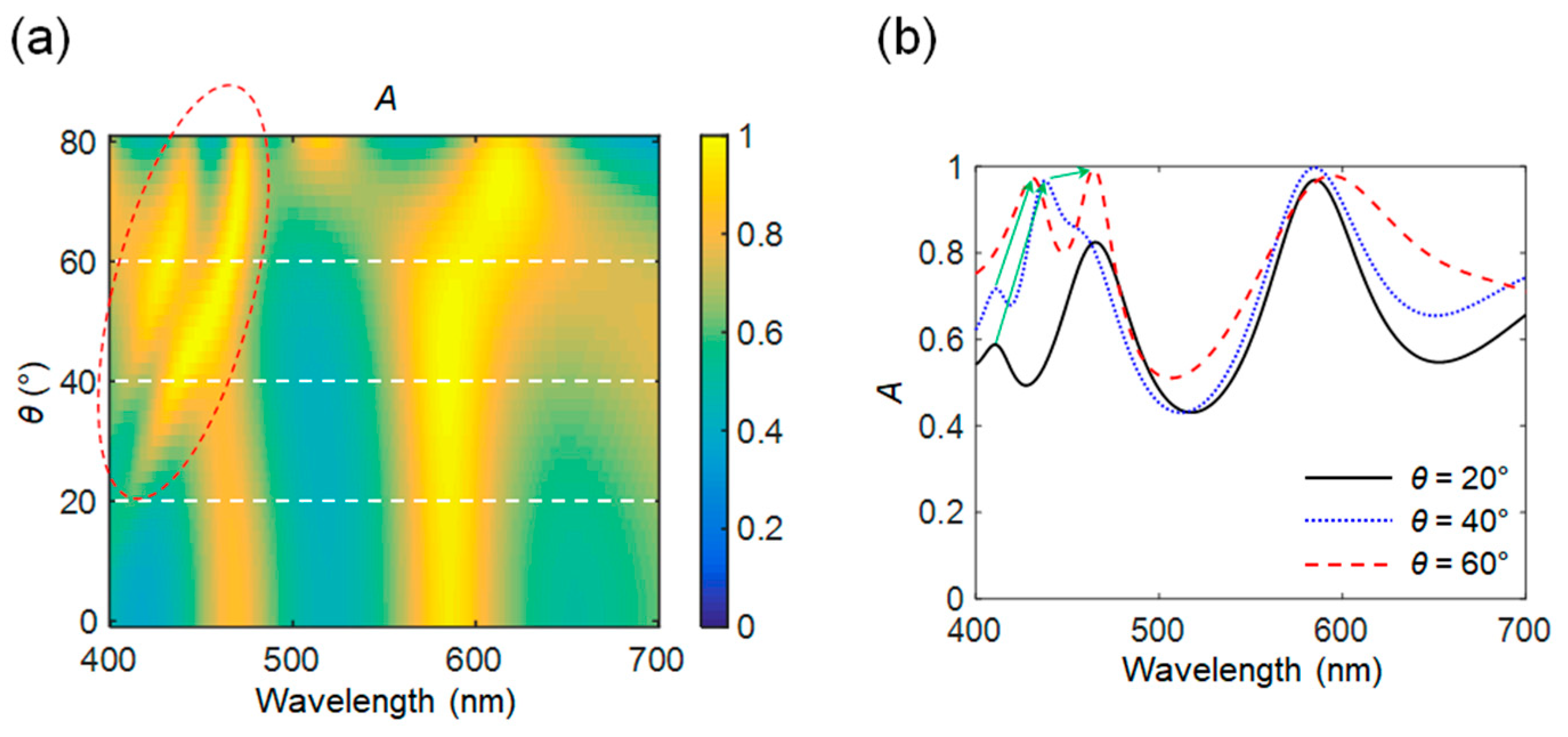
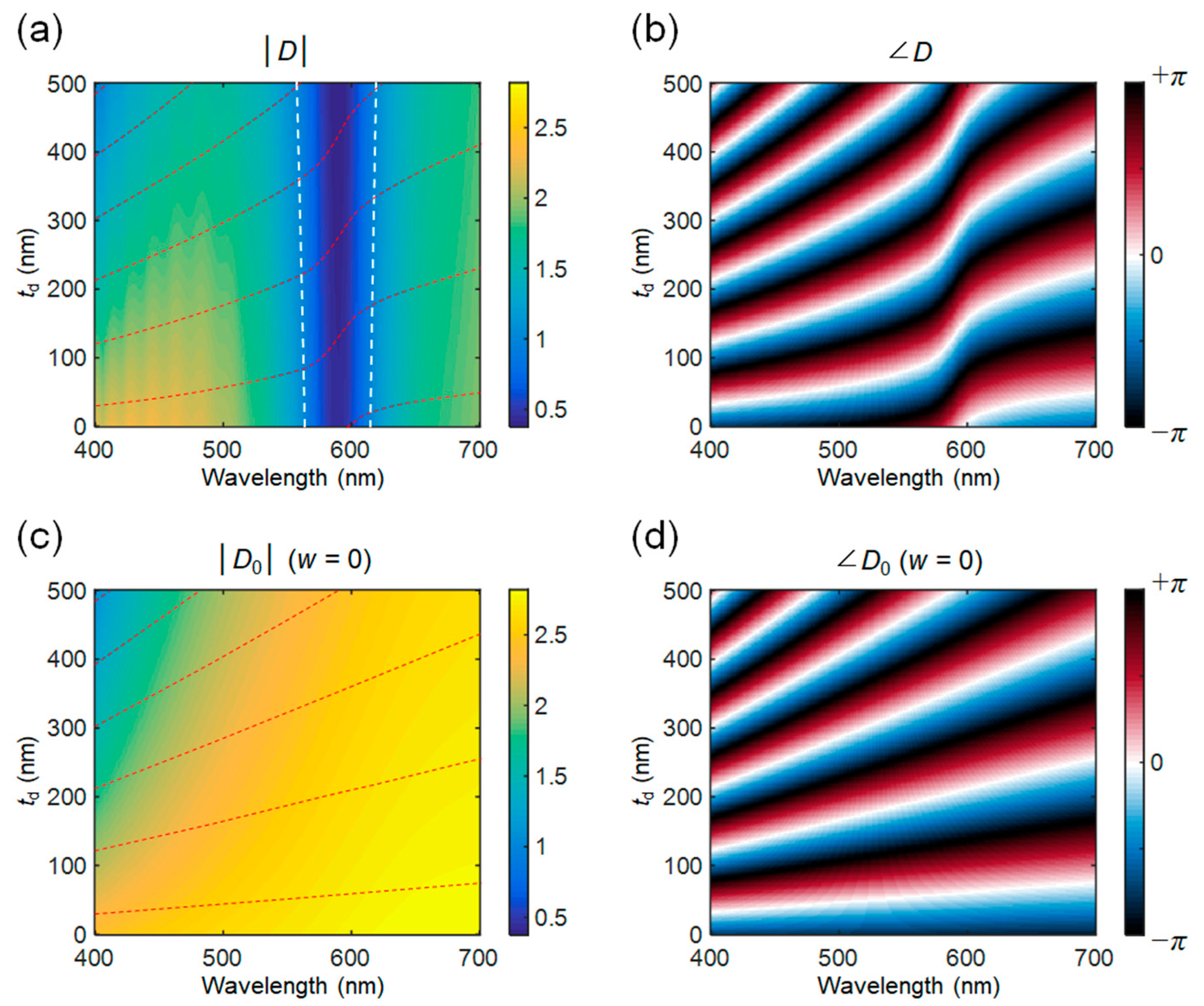
3. Conditions for Complete Optical Absorption by Critical Coupling

Examining the critical coupling behavior can be useful for obtaining perfect absorption at a desired frequency. Perfect absorption occurs when the overall reflectance of the structure is zero, which can be derived from the Equation (1) as
r 12   = r eff ( r 12 r 21 t 12 t 21 ) exp ( i 2 k 0 n ˜ ITO t d )
To find the conditions satisfying the Equation (2), we define the function D(td,λ) as follows:
D ( t d , λ ) = ( r eff / r 12 ) ( r 12 r 21 t 12 t 21 ) exp ( i 2 k 0 n ˜ ITO t d ) .
In Equation (3), the critical coupling condition is satisfied for td and λ that forces the magnitude and phase of D(td,λ) to be 1 and the integer multiples of 2π, respectively. Figure 7a,b show the magnitude and phase plots of D(td,λ). In Figure 7a, the white-colored and red-colored dashed lines indicate where the magnitude and phase of D(td,λ) are 1 and 2πm(m being an integer), respectively. The points where two dashed lines cross correspond to the unity absorption. These points are distributed near 590 nm, at which the magnitude of the reflection coefficient between the ITO and grating (reff) is minimized. For comparison, the magnitude and phase of D0(td,λ) for a flat Al reflector (w = 0) are presented in Figure 7c,d, respectively. Here, D0(td,λ) can be achieved by replacing reff as r0 = ( n ˜ ITO n ˜ Al ) / ( n ˜ ITO + n ˜ Al ) in Equation (3), where n ˜ Al represents the complex refractive index of Al. As can be seen from the plots, perfect absorption is unattainable in our calculation range without the subwavelength grating reflector since the unity magnitude condition on D0(td,λ) cannot be fulfilled. By exploiting this tendency, we can determine the structural parameters of visible light absorbers with desired absorption profiles.

4. Conclusions

We numerically investigated light absorption in metallic subwavelength gratings covered with a lossy dielectric medium. TMM was used to simulate the structure, where ITO and Al were chosen for a lossy dielectric and metal, respectively. The results show that subwavelength grating reflectors can be considered as semi-infinite homogeneous effective media whose optical responses can be obtained through numerical calculation. Based on these results, light absorption in dielectric-coated subwavelength gratings was calculated using an analytic expression for the reflectance of an asymmetric FP resonant cavity. Comparative numerical simulations allow us to determine how the coated dielectric film and subwavelength grating contribute to overall absorption. In addition, perfect absorption conditions were studied, revealing that the subwavelength grating structure can support critical coupling by acting as a dispersive absorbing substrate, which can be artificially engineered. We are convinced that our numerical study will provide a useful reference for designing subwavelength grating-based optical devices.

Author Contributions

Conceptualization, C.-Y.H.; Numerical Simulation, C.-Y.H.; Discussion, C.-Y.H., Y.-H.K., J.H.C., C.S.H.; Writing-Original Draft Preparation, C.-Y.H.; Writing-Review & Editing, C.-Y.H., Y.H.K., J.H.C., G.H.K., J.-H.Y., J.-E.P., H.-O.K., C.-S.H.; Project Administration, Y.-H.K.; C.-S.H.

Funding

This research was funded by the Korea government (MSIT).

Acknowledgments

This work was supported by The Cross-Ministry Giga KOREA Project (1711073921, Development of Telecommunications Terminal with Digital Holographic Table-top Display) and (1711072846, Development of Full-3D Mobile Display Terminal and Its Contents).

Conflicts of Interest

The authors declare no conflict of interest.

References

  1. Cui, Y.; He, Y.; Jin, Y.; Ding, F.; Yang, L.; Ye, Y.; Zhong, S.; Lin, Y.; He, S. Plasmonic and metamaterial structures as electromagnetic absorbers. Laser Photonics Rev. 2014, 8, 495–520. [Google Scholar] [CrossRef] [Green Version]
  2. Hedayati, M.K.; Faupel, F.; Elbahri, M. Review of plasmonic nanocomposite metamaterial absorber. Materials 2014, 7, 1221–1248. [Google Scholar] [CrossRef] [PubMed]
  3. Watts, C.M.; Liu, X.; Padilla, W.J. Metamaterial electromagnetic wave absorbers. Adv. Mater. 2012, 24, OP98–OP120. [Google Scholar] [CrossRef] [PubMed]
  4. Alaee, R.; Albooyeh, M.; Rockstuhl, C. Theory of metasurface based perfect absorbers. J. Phys. D. 2017, 50, 503002. [Google Scholar] [CrossRef] [Green Version]
  5. Kats, M.A.; Capasso, F. Optical absorbers based on strong interference in ultra-thin films. Laser Photonics Rev. 2016, 10, 735–749. [Google Scholar] [CrossRef] [Green Version]
  6. Atwater, H.A.; Polman, A. Plasmonics for improved photovoltaic devices. Nat. Mater. 2010, 9, 205–213. [Google Scholar] [CrossRef] [PubMed]
  7. Brongersma, M.L.; Cui, Y.; Fan, S. Light management for photovoltaics using high-index nanostructures. Nat. Mater. 2014, 13, 451–460. [Google Scholar] [CrossRef] [PubMed]
  8. Guo, C.F.; Sun, T.; Cao, F.; Liu, Q.; Ren, Z. Metallic nanostructures for light trapping in energy-harvesting devices. Light Sci. Appl. 2014, 3, e161. [Google Scholar]
  9. Sergeant, N.P.; Agrawal, M.; Peumans, P. High performance solar-selective absorbers using coated subwavelength gratings. Opt. Express 2010, 18, 5525–5540. [Google Scholar] [CrossRef] [PubMed]
  10. Azad, A.K.; Kort-Kamp, W.J.M.; Sykora, M.; Weisse-Bernstein, N.R.; Luk, T.S.; Taylor, A.J.; Dalvit, D.A.R.; Chen, H.T. Metasurface Broadband Solar Absorber. Sci. Rep. 2016, 6, 20347. [Google Scholar] [CrossRef] [PubMed] [Green Version]
  11. Lee, K.T.; Seo, S.; Guo, L.J. High-color-purity subtractive color filters with a wide viewing angle based on plasmonic perfect absorbers. Adv. Mater. 2015, 3, 347–352. [Google Scholar] [CrossRef]
  12. Kats, M.A.; Blanchard, R.; Genevet, P.; Capasso, F. Nanometre optical coatings based on strong interference effects in highly absorbing media. Nat. Mater. 2012, 12, 20–24. [Google Scholar] [CrossRef] [PubMed]
  13. Li, Z.; Butun, S.; Aydin, K. Large-area, lithography-free super absorbers and color filters at visible frequencies using ultrathin metallic films. ACS Photonics 2015, 2, 183–188. [Google Scholar] [CrossRef]
  14. Hwang, C.Y.; Yi, Y.; Choi, C.G. Reflection-type spatial amplitude modulation of visible light based on a sub-wavelength plasmonic absorber. Opt. Lett. 2016, 41, 990–993. [Google Scholar] [CrossRef] [PubMed]
  15. Hwang, C.Y.; Lee, S.Y.; Kim, Y.H.; Kim, T.Y.; Kim, G.H.; Yang, J.H.; Pi, J.E.; Choi, J.H.; Choi, K.; Kim, H.O.; et al. Switchable subwavelength plasmonic structures with phase-change materials for reflection-type active metasurfaces in the visible region. Appl. Phys. Lett. 2017, 10, 122201. [Google Scholar] [CrossRef] [Green Version]
  16. Liu, N.; Mesch, M.; Weiss, T.; Hentschel, M.; Giessen, H. Infrared perfect absorber and its application as plasmonic sensor. Nano Lett. 2010, 10, 2342–2348. [Google Scholar] [CrossRef] [PubMed]
  17. Dhawan, A.; Canva, M.; Vo-Dinh, T. Narrow groove plasmonic nano-gratings for surface plasmon resonance sensing. Opt. Express 2011, 19, 787–813. [Google Scholar] [CrossRef] [PubMed]
  18. Zhou, W.; Li, K.; Song, C.; Hao, P.; Chi, M.; Yu, M.; Wu, Y. Polarization-independent and omnidirectional nearly perfect absorber with ultra-thin 2D subwavelength metal grating in the visible region. Opt. Express 2015, 23, A413–A418. [Google Scholar] [CrossRef] [PubMed]
  19. Suen, J.Y.; Fan, K.; Montoya, J.; Bingham, C.; Stenger, V.; Sriram, S.; Padilla, W.J. Multifunctional metamaterial pyroelectric infrared detectors. Optica 2017, 4, 276–279. [Google Scholar] [CrossRef]
  20. Hao, J.M.; Wang, J.; Liu, X.L.; Padilla, W.J.; Zhou, L.; Qiu, M. High performance optical absorber based on a plasmonic metamaterial. Appl. Phys. Lett. 2010, 96, 251104. [Google Scholar] [CrossRef]
  21. Aydin, K.; Ferry, V.E.; Briggs, R.M.; Atwater, H.A. Broadband polarization-independent resonant light absorption using ultrathin plasmonic super absorbers. Nat. Commun. 2011, 2, 517. [Google Scholar] [CrossRef] [PubMed] [Green Version]
  22. Deng, H.; Li, Z.; Stan, L.; Rosenmann, D.; Czaplewski, D.; Gao, J.; Yang, X. Broadband perfect absorber based on one ultrathin layer of refractory metal. Opt. Lett. 2015, 40, 2592–2595. [Google Scholar] [CrossRef] [PubMed]
  23. Shu, S.; Li, Z.; Li, Y.Y. Triple-layer Fabry-Perot absorber with near-perfect absorption in visible and near-infrared regime. Opt. Express 2013, 21, 25307–25315. [Google Scholar] [CrossRef] [PubMed]
  24. Landy, N.I.; Sajuyigbe, S.; Mock, J.J.; Smith, D.R.; Padilla, W.J. Perfect Metamaterial Absorber. Phys. Rev. Lett. 2008, 100, 207402. [Google Scholar] [CrossRef] [PubMed]
  25. Liu, X.; Starr, T.; Starr, A.F.; Padilla, W.J. Infrared Spatial and Frequency Selective Metamaterial with Near-Unity Absorbance. Phys. Rev. Lett. 2010, 104, 207403. [Google Scholar] [CrossRef] [PubMed]
  26. Zhang, B.; Hendrickson, J.; Guo, J. Multispectral near-perfect metamaterial absorbers using spatially multiplexed plasmon resonance metal square structures. J. Opt. Soc. Am. B 2013, 30, 656–662. [Google Scholar] [CrossRef]
  27. Sun, J.; Liu, L.; Dong, G.; Zhou, J. An extremely broad band metamaterial absorber based on destructive interference. Opt. Express 2011, 19, 21155–21162. [Google Scholar] [CrossRef] [PubMed]
  28. Chen, H.T. Interference theory of metamaterial perfect absorbers. Opt. Express 2012, 20, 7165–7172. [Google Scholar] [CrossRef] [PubMed]
  29. Hao, J.; Zhou, L.; Qiu, M. Nearly total absorption of light and heat generation by plasmonic metamaterials. Phys. Rev. B 2011, 83, 165107. [Google Scholar] [CrossRef]
  30. Guo, W.; Liu, Y.; Han, T. Ultra-broadband infrared metasurface absorber. Opt. Express 2016, 24, 20586–20592. [Google Scholar] [CrossRef] [PubMed]
  31. Kats, M.A.; Sharma, D.; Lin, J.; Genevet, P.; Blanchard, R.; Yang, Z.; Qazilbash, M.M.; Basov, D.N.; Ramanathan, S.; Capasso, F. Ultra-thin perfect absorber employing a tunable phase change material. Appl. Phys. Lett. 2012, 101, 221101. [Google Scholar] [CrossRef]
  32. Long, Y.; Su, R.; Wang, Q.; Shen, L.; Li, B.; Zheng, W. Deducing critical coupling condition to achieve perfect absorption for thin-film absorbers and identifying key characteristics of absorbing materials needed for perfect absorption. Appl. Phys. Lett. 2014, 104, 091109. [Google Scholar] [CrossRef]
  33. Le Perchec, J.; Quémerais, P.; Barbara, A.; López-Ríos, T. Why metallic surfaces with grooves a few nanometers deep and wide may strongly absorb visible light. Phys. Rev. Lett. 2008, 100, 066408. [Google Scholar] [CrossRef] [PubMed]
  34. Chern, R.L.; Chen, Y.T.; Lin, H.Y. Anomalous optical absorption in metallic gratings with subwavelength slits. Opt. Express 2010, 18, 19510–19521. [Google Scholar] [CrossRef] [PubMed]
  35. Zhai, Y.; Chen, G.; Xu, J.; Qi, Z.; Li, X.; Wang, Q. Multiple-band perfect absorbers based on the combination of Fabry–Perot resonance and the gap plasmon resonance. Opt. Commun. 2017, 399, 28–33. [Google Scholar] [CrossRef]
  36. Lin, C.H.; Chern, R.L.; Lin, H.Y. Polarization-independent broad-band nearly perfect absorbers in the visible regime. Opt. Express 2011, 19, 415–424. [Google Scholar] [CrossRef] [PubMed]
  37. Wu, T.; Lai, J.; Wang, S.; Li, X.; Huang, Y. UV-visible broadband wide-angle polarization-insensitive absorber based on metal groove structures with multiple depths. Appl. Opt. 2017, 56, 5844–5848. [Google Scholar] [CrossRef] [PubMed]
  38. Miyazaki, H.T.; Kurokawa, Y. Squeezing visible light waves into a 3-nm-thick and 55-nm-long plasmon cavity. Phys. Rev. Lett. 2006, 96, 097401. [Google Scholar] [CrossRef] [PubMed]
  39. Kurokawa, Y.; Miyazaki, H.T. Metal-insulator-metal plasmon nanocavities: Analysis of optical properties. Phys. Rev. B 2007, 75, 035411. [Google Scholar] [CrossRef]
  40. Genet, G.; Ebbesen, T.W. Light in tiny holes. Nature 2007, 445, 39–46. [Google Scholar] [CrossRef] [PubMed]
  41. Garcia-Vidal, F.J.; Martin-Moreno, L.; Ebbesen, T.W.; Kuipers, L. Light passing through subwavelength apertures. Rev. Mod. Phys. 2010, 82, 729–787. [Google Scholar] [CrossRef] [Green Version]
  42. Porto, J.A.; Garcia-Vidal, F.J.; Pendry, J.B. Transmission resonances on metallic gratings with very narrow slits. Phys. Rev. Lett. 1999, 83, 2845–2848. [Google Scholar] [CrossRef]
  43. Neutens, P.; Van Dorpe, P.; De Vlaminck, I.; Lagae, L.; Borghs, G. Electrical detection of confined gap plasmons in metal–insulator–metal waveguides. Nat. Photonics 2009, 3, 283–286. [Google Scholar] [CrossRef]
  44. Schuller, J.A.; Barnard, E.S.; Cai, W.; Jun, Y.C.; White, J.S.; Brongersma, M.L. Plasmonics for extreme light concentration and manipulation. Nat. Mater. 2010, 9, 193–204. [Google Scholar] [CrossRef] [PubMed]
  45. White, J.S.; Veronis, G.; Yu, Z.; Barnard, E.S.; Chandran, A.; Fan, S.; Brongersma, M.L. Extraordinary optical absorption through subwavelength slits. Opt. Lett. 2009, 34, 686–688. [Google Scholar] [CrossRef] [PubMed]
  46. Chen, S.; Li, G.; Wong, W.; Pun, E.Y.B.; Cheah, K.K. Sharp plasmonic resonance on gold gratings in amplitude and phase domains. Appl. Opt. 2012, 51, 8563–8566. [Google Scholar] [CrossRef] [PubMed]
  47. Ikeda, K.; Miyazaki, H.T.; Kasaya, T.; Yamamoto, K.; Inoue, Y.; Fujimura, K.; Kanakugi, T.; Okada, M.; Hatade, K.; Kitagawa, S. Controlled thermal emission of polarized infrared waves from arrayed plasmon nanocavities. Appl. Phys. Lett. 2008, 92, 021117. [Google Scholar] [CrossRef]
  48. Miyazaki, H.T.; Ikeda, K.; Kasaya, T.; Yamamoto, K.; Inoue, Y.; Fujimura, K.; Kanakugi, T.; Okada, M.; Hatade, K.; Kitagawa, S. Thermal emission of two-color polarized infrared waves from integrated plasmon cavities. Appl. Phys. Lett. 2008, 92, 141114. [Google Scholar] [CrossRef]
  49. Bouchon, P.; Pardo, F.; Portier, B.; Ferlazzo, L.; Ghenuche, P.; Dagher, G.; Dupuis, C.; Bardou, N.; Haïdar, R.; Pelouard, J. Total funneling of light in high aspect ratio plasmonic nanoresonators. Appl. Phys. Lett. 2011, 98, 191109. [Google Scholar] [CrossRef]
  50. Ogawa, S.; Kimata, M. Direct fabrication and characterization of high-aspect-ratio plasmonic nanogratings using tapered-sidewall molds. Opt. Mater. Express 2017, 7, 633–640. [Google Scholar] [CrossRef]
  51. Kim, H.; Park, J.; Lee, B. Fourier Modal Method and Its Applications in Computational Nanophotonics, 1st ed.; CRC Press: Boca Raton, Florida, USA, 2012. [Google Scholar]
  52. Born, M.; Wolf, E. Principles of Optics: Electromagnetic Theory of Propagation, Interference and Diffraction of Light; Cambridge University Press: Cambridge, UK, 1999. [Google Scholar]
Figure 1. (a) A subwavelength metallic grating coated with a dielectric layer. The thicknesses of the upper dielectric layer and grating are td and tg, respectively. (b) The optically equivalent model, in which the grating and substrate are replaced by a semi-infinite effective medium.
Applsci 08 01445 g001
Figure 2. (a) Calculation geometry for determining reflection and phase shift characteristics in the subwavelength Al grating covered with ITO. (b) Spectral reflectance and (c) phase shift of the metallic grating for normally illuminated visible light (θ = 0) with respect to grating thicknesses ranging from 0 to 70 nm.
Applsci 08 01445 g002
Figure 3. (a) Diagram showing the reflection and transmission coefficients for calculation of the optical response of the metallic grating coated with a lossy dielectric using the numerical effective medium approach. (b) Experimentally measured optical constants of ITO and Al. (c) Magnitude and (d) phase profiles of the reflection coefficient at the interface between ITO and effective medium. (e) Magnitude and (f) phase profiles of the Fresnel reflection coefficients, and (g) magnitude and (h) phase profiles of the Fresnel transmission coefficients at the interface between air and ITO. All coefficients are calculated for normally incident light at visible frequencies.
Applsci 08 01445 g003
Figure 4. (a) Spectral absorption in the visible region with respect to the thickness of the upper dielectric medium deposited on the Al subwavelength grating (p = 160 nm, w = 40 nm, tg = 30 nm), and (b) corresponding map for a flat Al reflector (w = 0). Spectral absorption profiles when td = 180 nm (c) with and (d) without the grating structure.
Applsci 08 01445 g004
Figure 5. Distributions of the magnetic field within the structure when (a) 470 and (b) 585 nm transverse magnetic (TM) polarized plane waves illuminate the structure at normal incidence. The structural parameters are p = 160 nm, w = 40 nm, tg = 30 nm, and td = 270 nm. The calculation domain includes two unit cell elements, and the color scale is properly normalized to compare the field magnitudes.
Applsci 08 01445 g005
Figure 6. (a) The spectral absorption map with respect to the incident angle up to 80°. The structural parameters are the same as those used in Figure 5 (p = 160 nm, w = 40 nm, tg = 30 nm, and td = 270 nm). Absorption modes generated at oblique incidence are marked with the dashed red-colored oval. (b) Absorption profiles for three incident angles of θ = 20, 40, and 60°. Absorption peak shifts of new modes with increasing incidence angle are indicated by green-colored arrows.
Applsci 08 01445 g006
Figure 7. Plots of (a) magnitude and (b) phase of D(td,λ) defined in Equation (3) in order to investigate the critical coupling condition for perfect absorption. (c) and (d) show the corresponding results for the case of a flat Al reflector without the grating structure (w = 0). In (a,c), white- and red-colored dashed lines indicate where the magnitude is 1 and the phase is 2πm (m is an integer), respectively.
Applsci 08 01445 g007

