Bias Stability Enhancement in Thin-Film Transistor with a Solution-Processed ZrO2 Dielectric as Gate Insulator

 , and
, and
Abstract
:1. Introduction
2. Materials and Methods
2.1. Preparation of ZrO2 Film
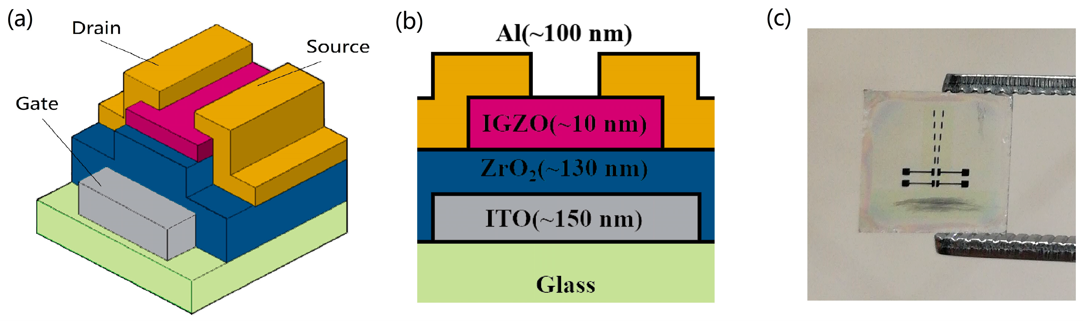
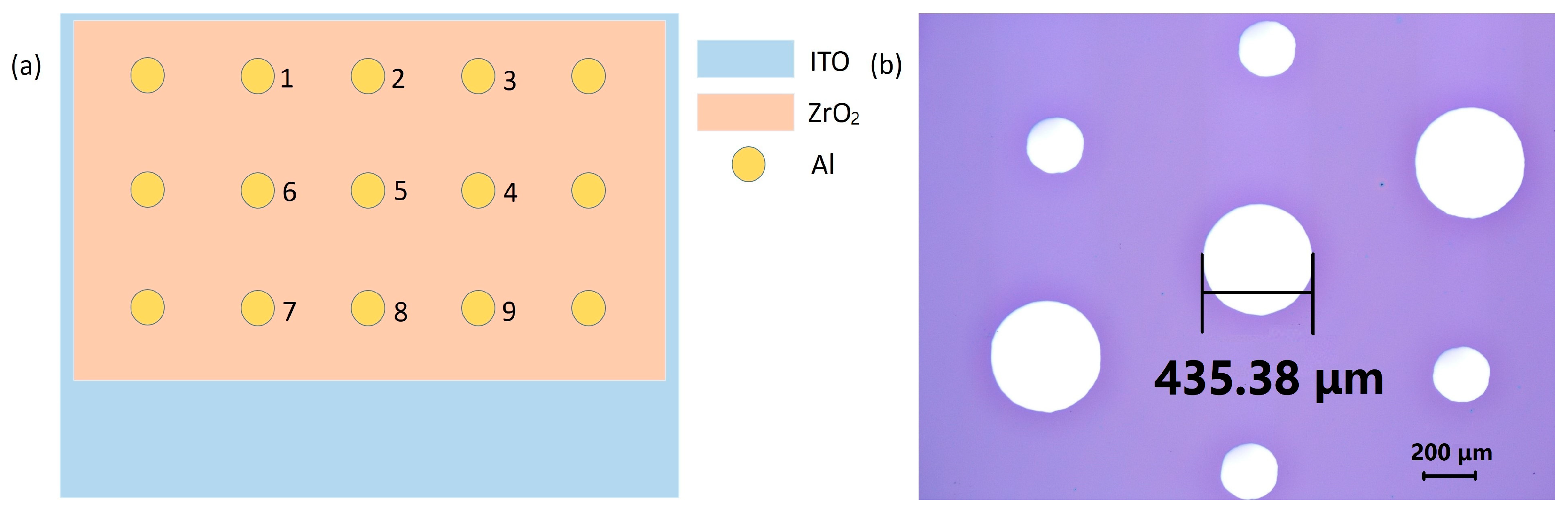
2.2. Fabrication of TFTs
2.3. Characterization
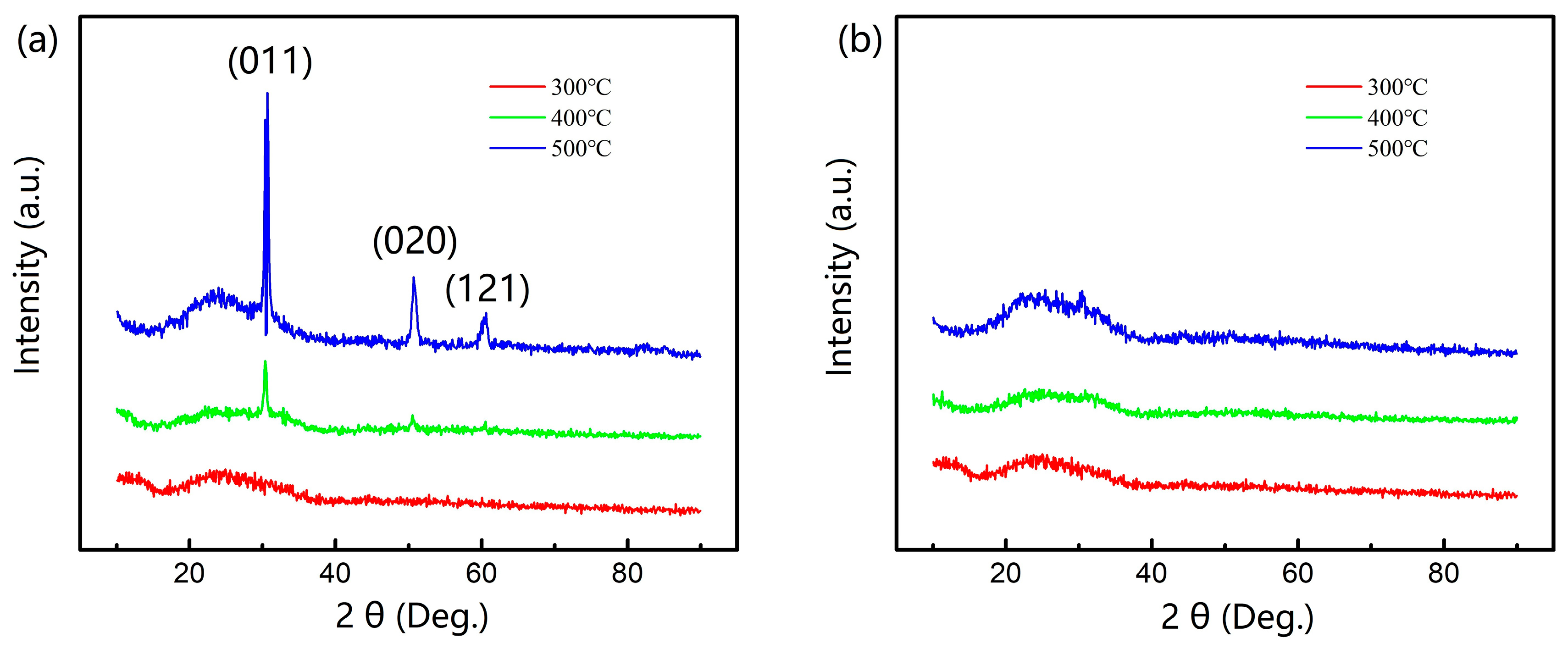
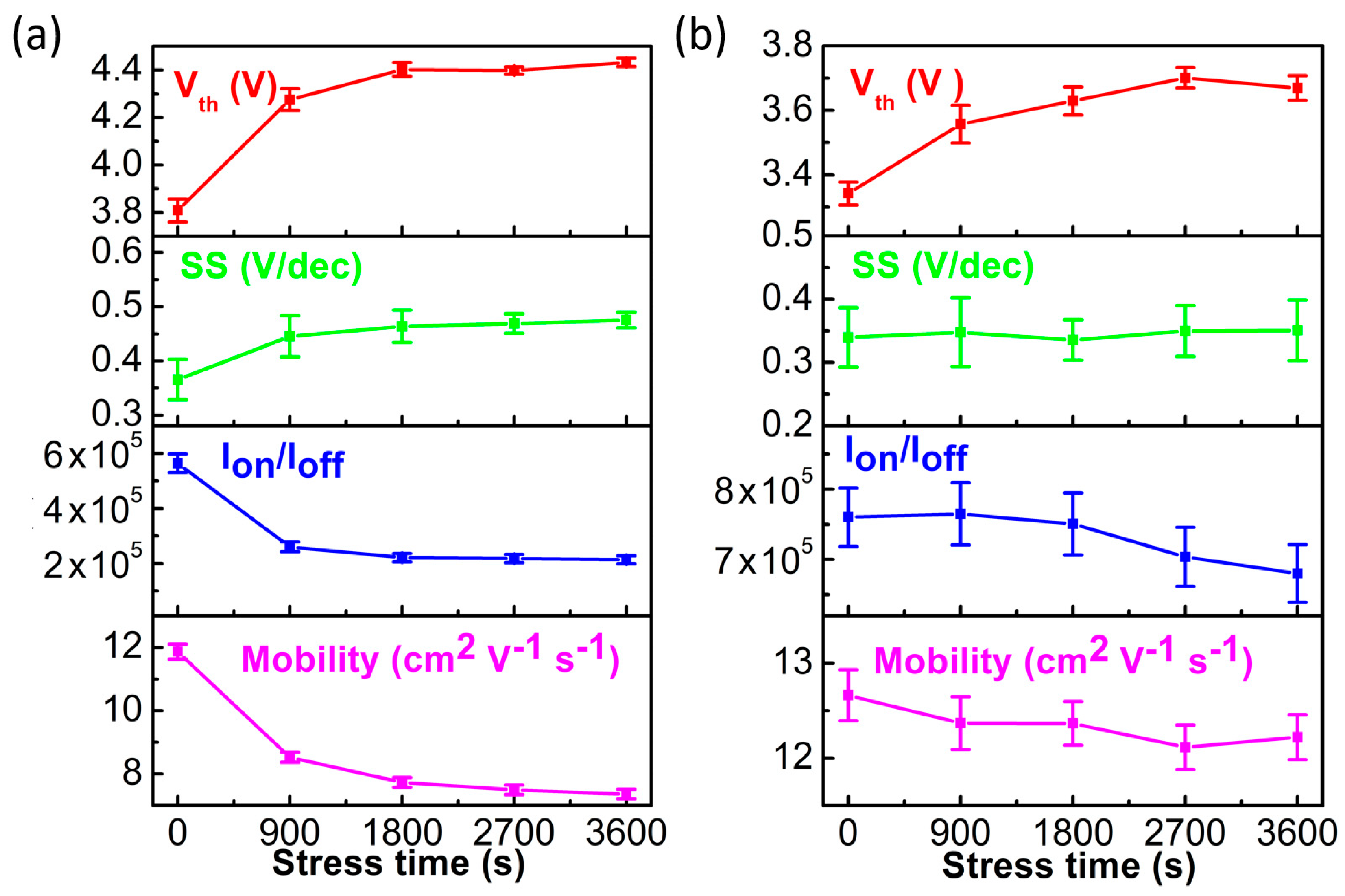
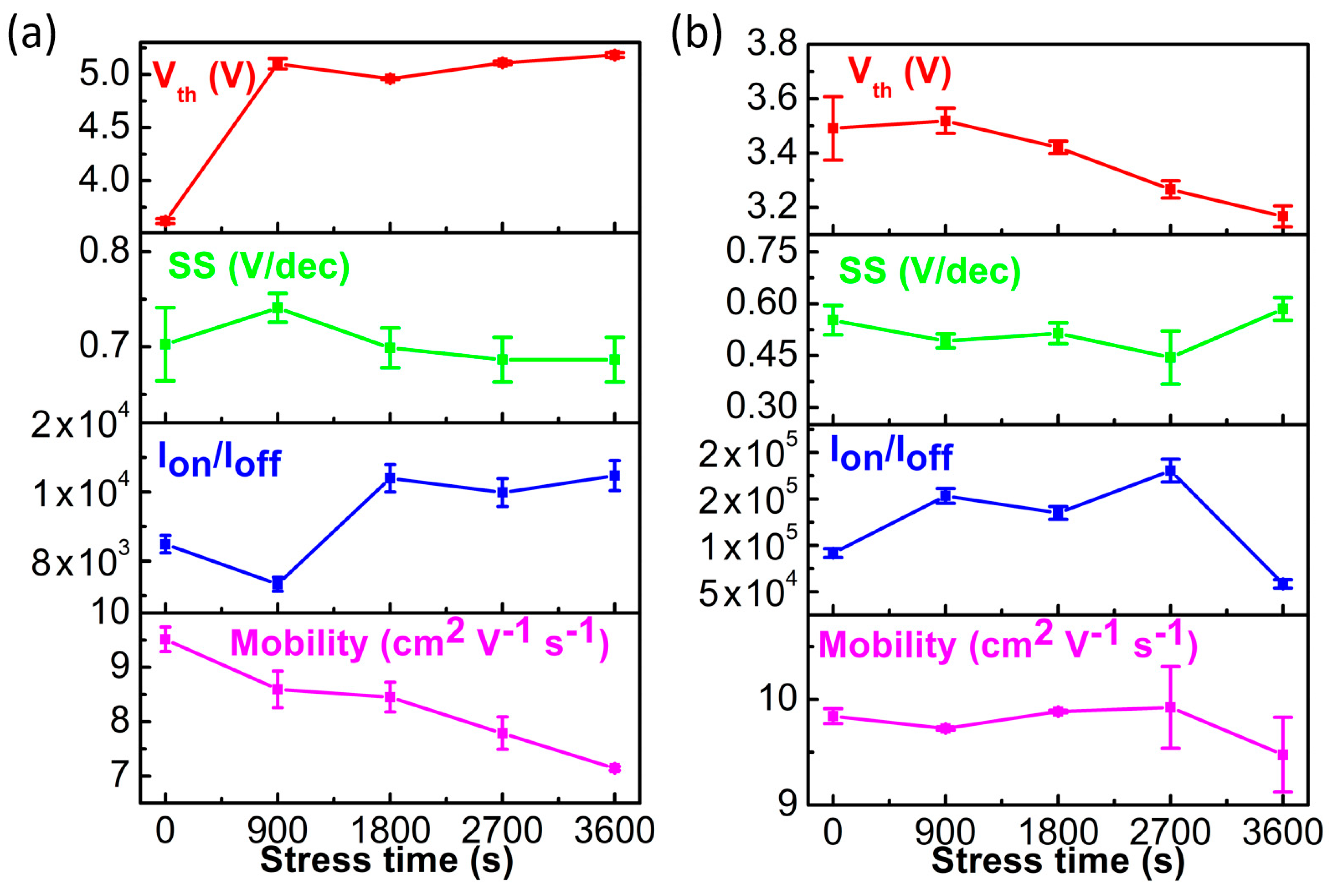
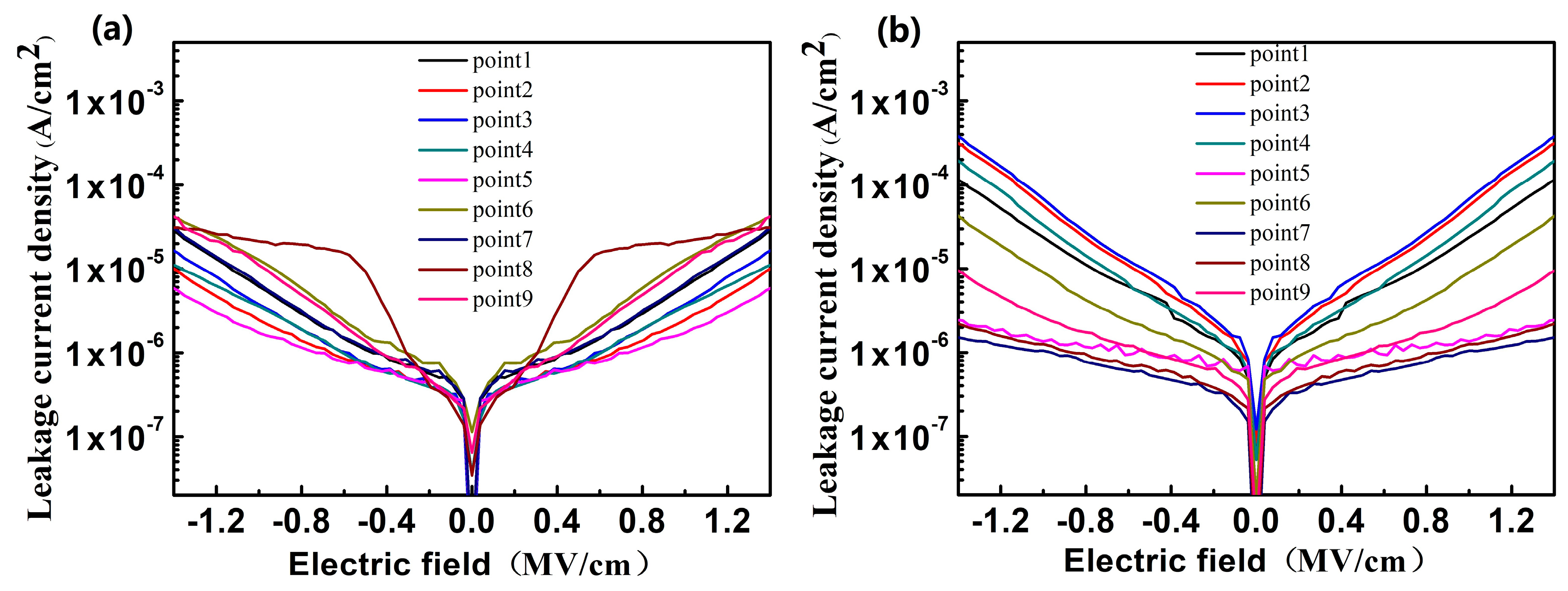
3. Results and Discussion
4. Conclusions
Author Contributions
Acknowledgments
Conflicts of Interest
References
- Park, J.S.; Maeng, W.-J.; Kim, H.-S.; Park, J.-S. Review of recent developments in amorphous oxide semiconductor thin-film transistor devices. Thin Solid Films 2012, 520, 1679–1693. [Google Scholar] [CrossRef]
- Fortunato, E.; Barquinha, P.; Martins, R. Oxide Semiconductor Thin-Film Transistors: A Review of Recent Advances. Adv. Mater. 2012, 24, 2945–2986. [Google Scholar] [CrossRef] [PubMed]
- Xu, W.; Dai, M.; Liang, L.; Liu, Z.; Sun, X.; Wan, Q.; Cao, H. Anomalous bias-stress-induced unstable phenomena of InZnO thin-film transistors using Ta2O5 gate dielectric. J. Phys. D Appl. Phys. 2012, 45. [Google Scholar] [CrossRef]
- Nomura, K.; Ohta, H.; Takagi, A.; Kamiya, T.; Hirano, M.; Hosono, H. Room-temperature fabrication of transparent flexible thin-film transistors using amorphous oxide semiconductors. Nature 2004, 432, 488–492. [Google Scholar] [CrossRef] [PubMed]
- Park, S.; Kim, C.-H.; Lee, W.-J.; Sung, S.; Yoon, M.-H. Sol-gel metal oxide dielectrics for all-solution-processed electronics. Mater. Sci. Eng. R Rep. 2017, 114, 1–22. [Google Scholar] [CrossRef]
- Li, X.F.; Xin, E.L.; Zhang, J.H. Low-Temperature Solution-Processed Zirconium Oxide Gate Insulators for Thin-Film Transistors. IEEE Trans. Electron Devices 2013, 60, 3413–3416. [Google Scholar]
- Chen, R.S.; Zhou, W.; Zhang, M.; Kwok, H.S. High performance self-aligned top-gate ZnO thin film transistors using sputtered Al2O3 gate dielectric. Thin Solid Films 2012, 520, 6681–6683. [Google Scholar] [CrossRef]
- Cho, J.; Choi, P.; Lee, N.; Kim, S.; Choi, B. Dielectric Properties of Solution-Processed ZrO2 for Thin-Film Transistors. J. Nanosci. Nanotechnol. 2016, 16, 10380–10384. [Google Scholar] [CrossRef]
- Lin, W.K.; Liu, K.C.; Chang, S.T.; Li, C.S. Room temperature fabricated transparent amorphous indium zinc oxide based thin film transistor using high-kappa HfO2 as gate insulator. Thin Solid Films 2012, 520, 3079–3083. [Google Scholar] [CrossRef]
- Bobade, S.M.; Shin, J.H.; Cho, Y.J.; You, J.S.; Choi, D.K. Room temperature fabrication Oxide TFT with Y2O3 as a gate oxide and Mo contact. Appl. Surf. Sci. 2009, 255, 7831–7833. [Google Scholar] [CrossRef]
- Liao, L.; Bai, J.; Lin, Y.-C.; Qu, Y.; Huang, Y.; Duan, X. High-Performance Top-Gated Graphene-Nanoribbon Transistors Using Zirconium Oxide Nanowires as High-Dielectric-Constant Gate Dielectrics. Adv. Mater. 2010, 22, 1941–1945. [Google Scholar] [CrossRef] [PubMed]
- Zhang, W.; Cui, Y.; Hu, Z.G.; Yu, W.L.; Sun, J.; Xu, N.; Ying, Z.F.; Wu, J.D. Structural, optical and electrical properties of high-k ZrO2 dielectrics on Si prepared by plasma assisted pulsed laser deposition. Thin Solid Films 2012, 520, 6361–6367. [Google Scholar] [CrossRef]
- Jang, J.; Kitsomboonloha, R.; Swisher, S.L.; Park, E.S.; Kang, H.; Subramanian, V. Transparent High-Performance Thin Film Transistors from Solution-Processed SnO2/ZrO2 Gel-like Precursors. Adv. Mater. 2013, 25, 1042–1047. [Google Scholar] [CrossRef] [PubMed]
- Lim, K.-H.; Huh, J.-E.; Lee, J.; Cho, N.-K.; Park, J.-W.; Nam, B.-I.; Lee, E.; Kim, Y.S. Strong Influence of Humidity on Low-Temperature Thin-Film Fabrication via Metal Aqua Complex for High Performance Oxide Semiconductor Thin-Film Transistors. ACS Appl. Mater. Interfaces 2017, 9, 548–557. [Google Scholar] [CrossRef] [PubMed]
- Lim, K.-H.; Lee, J.; Huh, J.-E.; Park, J.; Lee, J.-H.; Lee, S.-E.; Kim, Y.S. A systematic study on effects of precursors and solvents for optimization of solution-processed oxide semiconductor thin-film transistors. J. Mater. Chem. C 2017, 5, 7768–7776. [Google Scholar] [CrossRef]
- Gong, Y.; Zhao, K.; He, H.; Cai, W.; Tang, N.; Ning, H.; Wu, S.; Gao, J.; Zhou, G.; Lu, X.; et al. Solution processable high quality ZrO2 dielectric films for low operation voltage and flexible organic thin film transistor applications. J. Phys. D Appl. Phys. 2018, 51. [Google Scholar] [CrossRef]
- Gong, Y.; Zhao, K.; Yan, L.; Wei, W.; Yang, C.; Ning, H.; Wu, S.; Gao, J.; Zhou, G.; Lu, X.; et al. Room Temperature Fabrication of High Quality ZrO2 Dielectric Films for High Performance Flexible Organic Transistor Applications. IEEE Electron Device Lett. 2018, 39, 280–283. [Google Scholar] [CrossRef]
- Naik, B.R.; Avis, C.; Chowdhury, M.D.H.; Kim, T.; Lin, T.; Jang, J. Improvement in performance of solution-processed indium-zinc-tin oxide thin-film transistors by UV/O3 treatment on zirconium oxide gate insulator. Jpn. J. Appl. Phys. 2016, 55. [Google Scholar] [CrossRef]
- Jeong, Y.; Bae, C.; Kim, D.; Song, K.; Woo, K.; Shin, H.; Cao, G.; Moon, J. Bias-Stress-Stable Solution-Processed Oxide Thin Film Transistors. ACS Appl. Mater. Interfaces 2010, 2, 611–615. [Google Scholar] [CrossRef] [PubMed]
- Kim, C.H.; Rim, Y.S.; Kim, H.J. The effect of a zinc-tin-oxide layer used as an etch-stopper layer on the bias stress stability of solution-processed indium-gallium-zinc-oxide thin-film transistors. J. Phys. D Appl. Phys. 2014, 47. [Google Scholar] [CrossRef]
- Yih-Shing, L.; Yu-Hsin, W.; Tsung-Cheng, T.; Tsung-Eong, H. Positive bias stress instability of In-Ga-Zn-O thin-film transistors with Al2O3/TEOS oxide gate dielectrics. In Proceedings of the 2017 24th International Workshop on Active-Matrix Flatpanel Displays and Devices, Kyoto, Japan, 4–7 July 2017; pp. 205–206. [Google Scholar]
- Kim, S.J.; Yoon, D.H.; Rim, Y.S.; Kim, H.J. Low-Temperature Solution-Processed ZrO2 Gate Insulators for Thin-Film Transistors Using High-Pressure Annealing. Electrochem. Solid State Lett. 2011, 14, E35–E37. [Google Scholar] [CrossRef]
- Liu, A.; Liu, G.X.; Zhu, H.H.; Xu, F.; Fortunato, E.; Martins, R.; Shan, F.K. Fully Solution-Processed Low-Voltage Aqueous In2O3 Thin-Film Transistors Using an Ultrathin ZrOx Dielectric. ACS Appl. Mater. Interfaces 2014, 6, 17364–17369. [Google Scholar] [CrossRef] [PubMed]
- Ha, T.-J.; Dodabalapur, A. Photo stability of solution-processed low-voltage high mobility zinc-tin-oxide/ZrO2 thin-film transistors for transparent display applications. Appl. Phys. Lett. 2013, 102. [Google Scholar] [CrossRef]
- Cai, W.; Zhu, Z.; Wei, J.; Fang, Z.; Ning, H.; Zheng, Z.; Zhou, S.; Yao, R.; Peng, J.; Lu, X. A Simple Method for High-Performance, Solution-Processed, Amorphous ZrO2 Gate Insulator TFT with a High Concentration Precursor. Materials 2017, 10. [Google Scholar] [CrossRef] [PubMed]
- Ding, X.; Zhang, J.; Zhang, H.; Ding, H.; Huang, C.; Li, J.; Shi, W.; Jiang, X.; Zhang, Z. ZrO2 insulator modified by a thin Al2O3 film to enhance the performance of InGaZnO thin-film transistor. Microelectron. Reliab. 2014, 54, 2401–2405. [Google Scholar] [CrossRef]
- Ding, X.; Zhang, H.; Zhang, J.; Li, J.; Shi, W.; Jiang, X.; Zhang, Z. IGZO thin film transistors with Al2O3 gate insulators fabricated at different temperatures. Mater. Sci. Semicond. Process. 2015, 29, 69–75. [Google Scholar] [CrossRef]
- Li, J.; Zhou, F.; Lin, H.-P.; Zhu, W.-Q.; Zhang, J.-H.; Jiang, X.-Y.; Zhang, Z.-L. Effect of reactive sputtered SiOx passivation layer on the stability of InGaZnO thin film transistors. Vacuum 2012, 86, 1840–1843. [Google Scholar] [CrossRef]
- Verlaak, S.; Arkhipov, V.; Heremans, P. Modeling of transport in polycrystalline organic semiconductor films. Appl. Phys. Lett. 2003, 82, 745–747. [Google Scholar] [CrossRef]
- Jeong, J.K.; Yang, H.W.; Jeong, J.H.; Mo, Y.G.; Kim, H.D. Origin of threshold voltage instability in indium-gallium-zinc oxide thin film transistors. Appl. Phys. Lett. 2008, 93. [Google Scholar] [CrossRef]
- Kim, D.J.; Kim, D.L.; Rim, Y.S.; Kim, C.H.; Jeong, W.H.; Lim, H.S.; Kim, H.J. Improved Electrical Performance of an Oxide Thin-Film Transistor Having Multistacked Active Layers Using a Solution Process. ACS Appl. Mater. Interfaces 2012, 4, 4001–4005. [Google Scholar] [CrossRef] [PubMed]


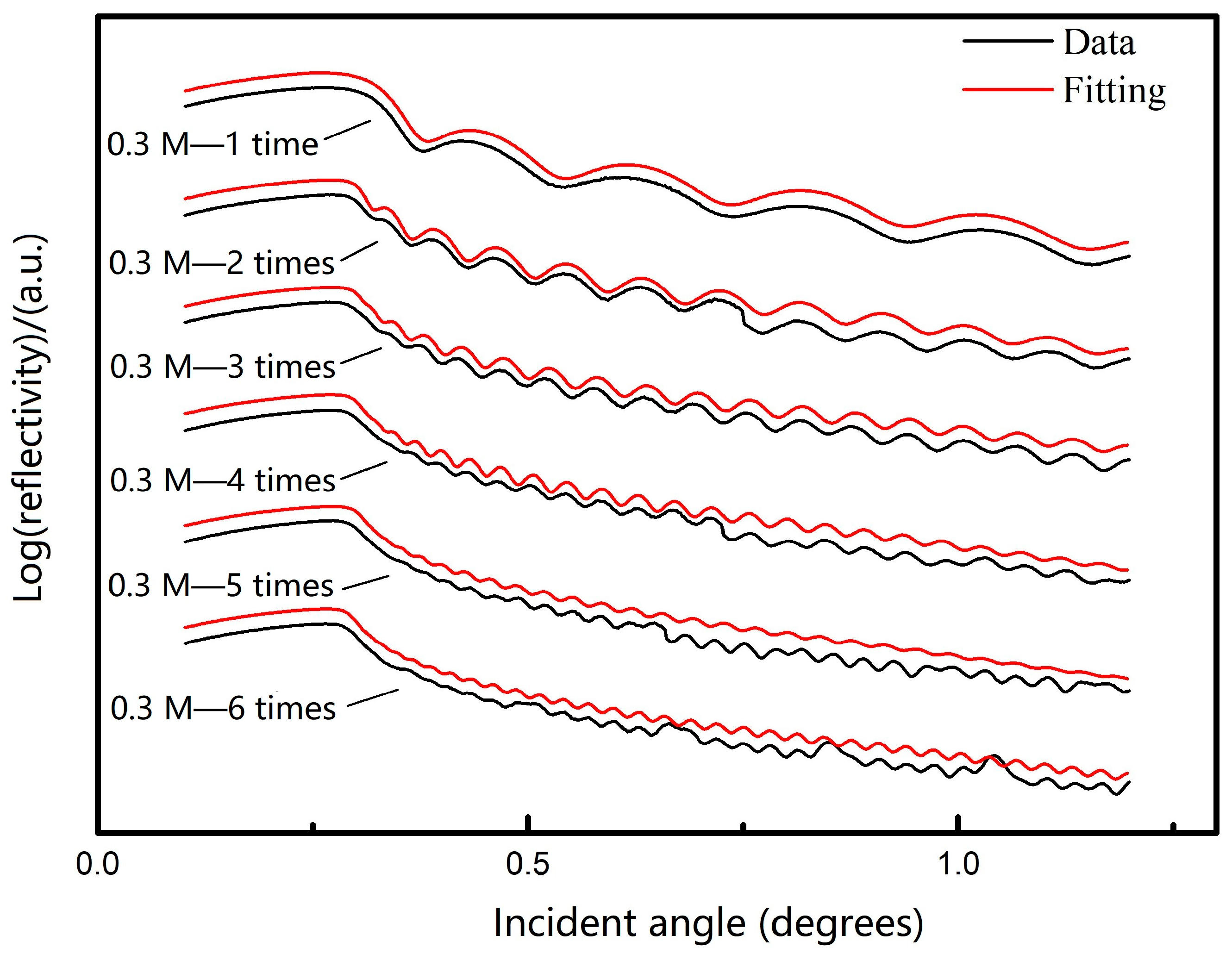
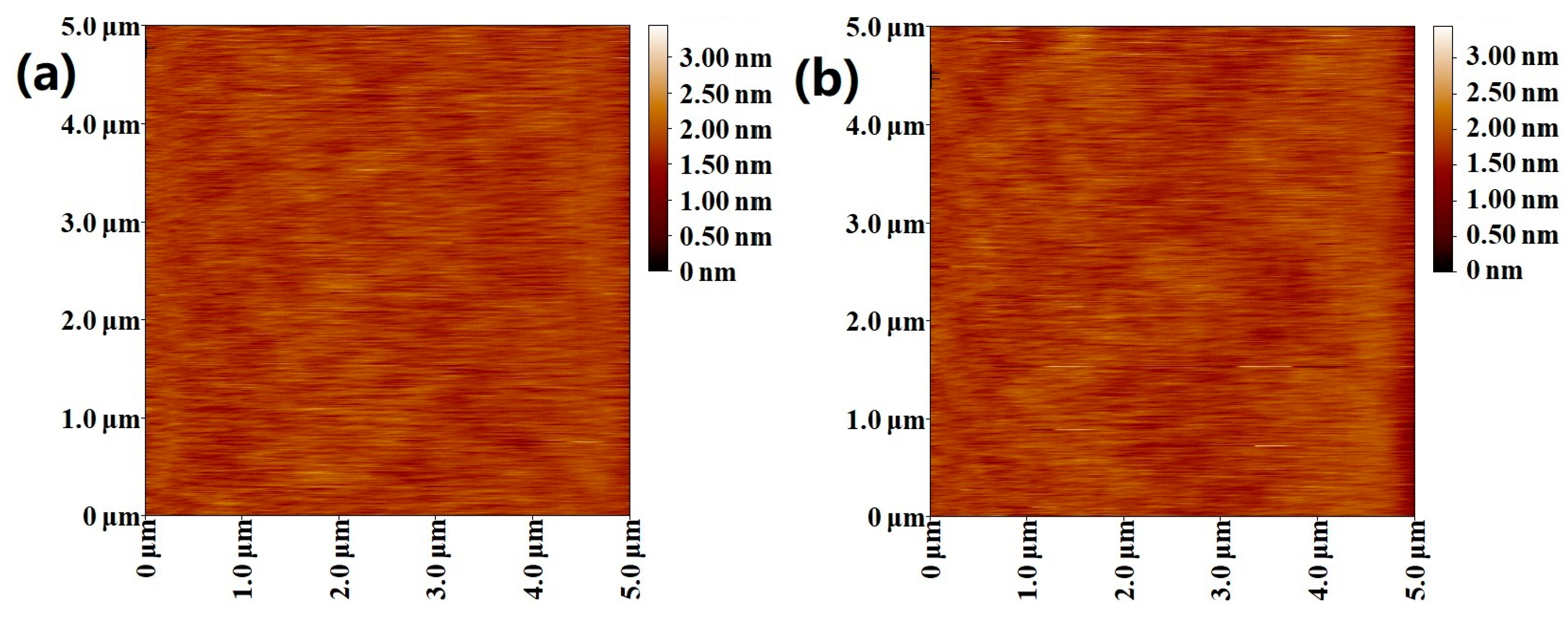
| Concentration | Layer | Density (g/cm3) | Thickness (nm) | Roughness (nm) |
|---|---|---|---|---|
| 0.3 M | 1 | 4.86 | 19.98 | 0.46 |
| 0.3 M | 2 | 4.70 | 43.53 | 0.46 |
| 0.3 M | 3 | 4.83 | 66.98 | 0.26 |
| 0.3 M | 4 | 4.78 | 91.61 | 0.49 |
| 0.3 M | 5 | 4.76 | 118.89 | 0.55 |
| 0.3 M | 6 | 4.77 | 129.29 | 0.41 |
| 0.6 M | 3 | 4.70 | 132.62 | 0.43 |
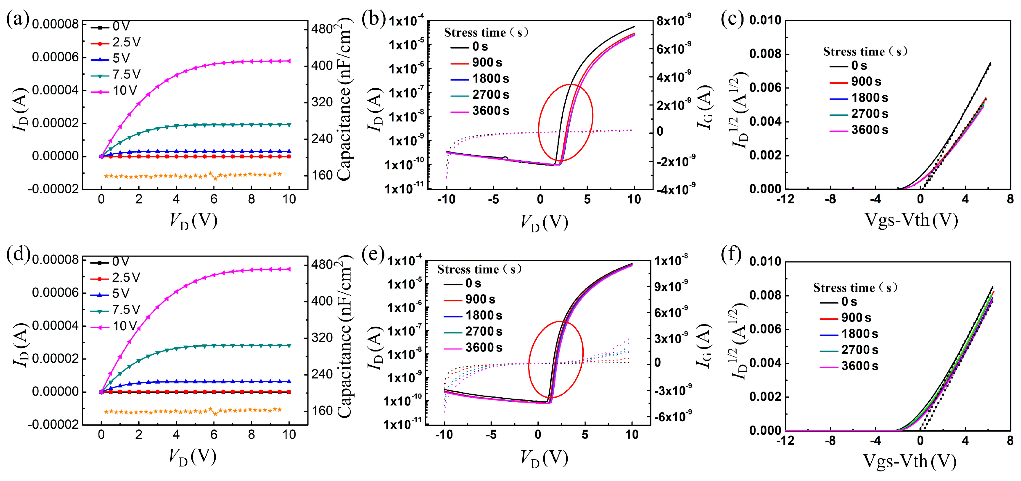
| Device | Stress Time (s) | Negative Bias Stress (NBS) | Positive Bias Stress (PBS) | ||||||
|---|---|---|---|---|---|---|---|---|---|
| μsat (cm2 V−1 s−1) | Ion/Ioff (×105) | SS (V/dec) | Vth (V) | μsat (cm2 V−1 s−1) | Ion/Ioff (× 105) | SS (V/dec) | Vth (V) | ||
| Device A | 0 | 12.7 ± 0.34 | 7.6 ± 0.51 | 0.34 ± 0.06 | 3.34 ± 0.05 | 11.9 ± 0.32 | 5.6 ± 0.42 | 0.37 ± 0.05 | 3.81 ± 0.07 |
| 900 | 12.4 ± 0.35 | 7.6 ± 0.55 | 0.35 ± 0.07 | 3.55 ± 0.08 | 8.5 ± 0.21 | 2.6 ± 0.22 | 0.45 ± 0.05 | 4.28 ± 0.06 | |
| 1800 | 12.3 ± 0.30 | 7.5 ± 0.55 | 0.34 ± 0.04 | 3.63 ± 0.06 | 7.7 ± 0.20 | 2.2 ± 0.19 | 0.46 ± 0.04 | 4.40 ± 0.04 | |
| 2700 | 12.2 ± 0.31 | 7.0 ± 0.52 | 0.35 ± 0.05 | 3.70 ± 0.04 | 7.5 ± 0.20 | 2.2 ± 0.19 | 0.47 ± 0.02 | 4.40 ± 0.02 | |
| 3600 | 12.1 ± 0.31 | 6.8 ± 0.50 | 0.35 ± 0.06 | 3.67 ± 0.05 | 7.4 ± 0.20 | 2.1 ± 0.18 | 0.48 ± 0.02 | 4.43 ± 0.02 | |
| Device B | 0 | 9.8 ± 0.10 | 0.92 ± 0.058 | 0.55 ± 0.06 | 3.49 ± 0.16 | 9.5 ± 0.28 | 0.090 ± 0.0062 | 0.70 ± 0.05 | 3.62 ± 0.03 |
| 900 | 9.7 ± 0.02 | 1.5 ± 0.098 | 0.49 ± 0.03 | 3.52 ± 0.06 | 8.6 ± 0.42 | 0.067 ± 0.0051 | 0.74 ± 0.02 | 5.10 ± 0.06 | |
| 1800 | 9.9 ± 0.02 | 1.3 ± 0.084 | 0.51 ± 0.04 | 3.42 ± 0.03 | 8.5 ± 0.37 | 0.13 ± 0.0098 | 0.70 ± 0.03 | 4.96 ± 0.01 | |
| 2700 | 9.9 ± 0.96 | 1.8 ± 0.15 | 0.44 ± 0.14 | 3.27 ± 0.04 | 7.8 ± 0.41 | 0.12 ± 0.0098 | 0.69 ± 0.03 | 5.11 ± 0.03 | |
| 3600 | 9.5 ± 0.48 | 0.58 ± 0.056 | 0.58 ± 0.04 | 3.17 ± 0.05 | 7.1 ± 0.04 | 0.13 ± 0.011 | 0.69 ± 0.03 | 5.18 ± 0.03 | |
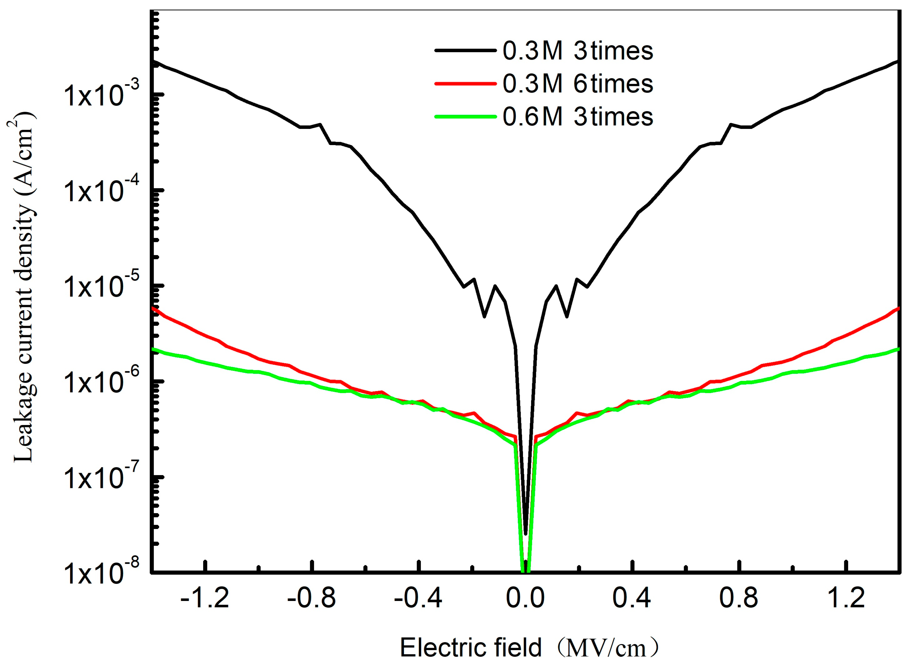
| ZrO2 Films | Leakage Current Density (A/cm2) (10 V) | |||
|---|---|---|---|---|
| Average Value | Maximum Value | Minimum Value | Standard Deviation | |
| 0.6 M precursor spin-coating 3 times | 6.9 × 10⁻⁶ | 2.1 × 10⁻⁵ | 5.1 × 10⁻⁷ | 7.8 × 10⁻⁶ |
| 0.3 M precursor spin-coating 6 times | 1.6 × 10⁻⁶ | 3.4 × 10⁻⁶ | 4.0 × 10⁻⁷ | 9.39 × 10⁻⁷ |
© 2018 by the authors. Licensee MDPI, Basel, Switzerland. This article is an open access article distributed under the terms and conditions of the Creative Commons Attribution (CC BY) license (http://creativecommons.org/licenses/by/4.0/).
Share and Cite
Zhou, S.; Fang, Z.; Ning, H.; Cai, W.; Zhu, Z.; Wei, J.; Lu, X.; Yuan, W.; Yao, R.; Peng, J. Bias Stability Enhancement in Thin-Film Transistor with a Solution-Processed ZrO2 Dielectric as Gate Insulator. Appl. Sci. 2018, 8, 806. https://doi.org/10.3390/app8050806
Zhou S, Fang Z, Ning H, Cai W, Zhu Z, Wei J, Lu X, Yuan W, Yao R, Peng J. Bias Stability Enhancement in Thin-Film Transistor with a Solution-Processed ZrO2 Dielectric as Gate Insulator. Applied Sciences. 2018; 8(5):806. https://doi.org/10.3390/app8050806
Chicago/Turabian StyleZhou, Shangxiong, Zhiqiang Fang, Honglong Ning, Wei Cai, Zhennan Zhu, Jinglin Wei, Xubing Lu, Weijian Yuan, Rihui Yao, and Junbiao Peng. 2018. "Bias Stability Enhancement in Thin-Film Transistor with a Solution-Processed ZrO2 Dielectric as Gate Insulator" Applied Sciences 8, no. 5: 806. https://doi.org/10.3390/app8050806