Article

Spin-Related Micro-Photoluminescence in Fe3+ Doped ZnSe Nanoribbons

1
Beijing Key Laboratory of Nanophotonics and Ultrafine Optoelectronic Systems, School of Physics, Beijing Institute of Technology, Beijing 100081, China
2
Wuhan National High Magnetic Field Center, School of physics, Huazhong University of Science and Technology, Wuhan 430074, China
*
Authors to whom correspondence should be addressed.
Appl. Sci. 2017, 7(1), 39; https://doi.org/10.3390/app7010039
Submission received: 19 October 2016 / Revised: 7 December 2016 / Accepted: 22 December 2016 / Published: 29 December 2016

Abstract

:
Spin-related emission properties have important applications in the future information technology; however, they involve microscopic ferromagnetic coupling, antiferromagnetic or ferrimagnetic coupling between transition metal ions and excitons, or d state coupling with phonons is not well understood in these diluted magnetic semiconductors (DMS). Fe3+ doped ZnSe nanoribbons, as a DMS example, have been successfully prepared by a thermal evaporation method. Their power-dependent micro-photoluminescence (PL) spectra and temperature-dependent PL spectra of a single ZnSe:Fe nanoribbon have been obtained and demonstrated that alio-valence ion doping diminishes the exciton magnetic polaron (EMP) effect by introducing exceeded charges. The d-d transition emission peaks of Fe3+ assigned to the 4T2 (G) → 6A1 (S) transition at 553 nm and 4T1 (G) → 6A1 (S) transition at 630 nm in the ZnSe lattice have been observed. The emission lifetimes and their temperature dependences have been obtained, which reflected different spin–phonon interactions. There exists a sharp decrease of PL lifetime at about 60 K, which hints at a magnetic phase transition. These spin–spin and spin–phonon interaction related PL phenomena are applicable in the future spin-related photonic nanodevices.

Graphical Abstract

1. Introduction

Information technology has advanced quickly to quantum-based units, which are usually realized in nanosized structures and are small in size, high in speed and consume less energy. In these nanostructures, electrons with more quantum characters except charges could be exploited and modulated to present specific properties with higher efficiency. For example, spin-related carriers and excitons in magnetic semiconductors are the typical excitations with the potential to be applied in future devices and have attracted much attention.
The ZnSe nanostructure is a type of important II–VI group semiconductor with a bandgap of about 2.7 eV at room temperature exhibiting excellent luminescence properties [1,2,3,4]. Since the 1990s, the investigations on the properties of ZnSe nanostructures, including optics, magnetism and transport properties, have been done well in many groups [5,6]. Specifically, transition metal ion doped ZnSe nano-materials, as a diluted magnetic semiconductor (DMS), have significant potential in optics and magnetic physics [7,8,9], and have been received much attention. Vlaskin et al. studied the tunable dual emission based on Mn doped ZnSe nanocrystals [10]. Wang et al. proposed that the interface between MnSe dopant and ZnSe host could be used for manipulating irradiative defects with a controllable manner [11]. In addition, the magnetic and luminescent properties of Fe doped ZnSe were also investigated by Kulyuk et al. [12]. The excellent emission properties of ZnSe nanostructures are potentially applicable for the lasing, lighting, and other optoelectronic devices [2,13,14,15].
The luminescence properties of transition metal doped semiconductor were influenced not only by the exciton recombination process but also spin-related interactions [16,17]. Researchers have found that the exchange interaction between transition metal ions in diluted magnetic semiconductors can modify their band-edge emission and d-d transition emission [18,19]. Kamran et al. reported that tunable emissions within the band gap is due to ferromagnetic coupling Mn(II) aggregates in Mn-doped CdS nanowires [20]. Norris et al. reported Mn doped ZnSe nanocrystals demonstrating large Zeeman splitting by magnetic circular dichroism [7]. Heitz et al. studied the Fe3+ doped ZnO crystal by means of emission, excitation, and magneto-optical spectroscopy, and showed that the d-d transition of isolated Fe3+ ions on Zn2+ lattice sites [21]. Traditionally, spin-related micro-photoluminescence study on DMS has significance for spin-related devices, bosonic laser and other spintronics applications, while alio-valence ions doped semiconductor compared with iso-valence ions show different optics and spin-related electrical properties.
In Fe3+ doped ZnSe nanoribbons, trivalent Fe ion substitutes for the divalent Zn ion site, which has a d5 configuration that is the same as the d configuration of Mn2+. In the cubic crystal field, the ground state 6S is labeled as 6A1 due to its spherically symmetric and non-degenerate characteristics, whereas the lowest excited state 4G splits into four levels, labeled as 4T1, 4T2, 4E and 4A1 [22]. Mainly, the unpaired redundant electrons in Fe3+ can impact the emission and spin-related properties in Fe doped ZnSe nanostructures [23]. In this paper, we have prepared high quality Fe3+ doped ZnSe nanoribbons and studied the temperature and power dependent emissions by micro-photoluminescence spectra and lifetime measurements, in which the spin–exciton interaction, spin–spin interaction and exciton–phonon coupling have been identified.

2. Experimental Section

Fe doped ZnSe nanoribbons were synthesized by the chemical vapor deposition (CVD) method with Au used as the catalyst. In addition, 0.8 g mixture of ZnSe (Alfa Aesar, Haver Hill, MA, USA, 99.99% purity) and Fe2O3 (Aladdin, 99.9%, Shanghai, China) powders, with a mass ratio of 20:1, were loaded in ceramic boat and inserted into the central region of the quartz tube mounted in the tube furnace. The cleaned mica pieces coated with about 10 nm thick Au layer were placed downstream of the quartz tube at a distance of 10 cm away from precursor. The high purity mixed gas with 10% hydrogen and 90% argon flowed through the quartz tube for one hour in order to purify the growth environment of nanoribbons. Then, the precursor was heated to 1150 °C for 90 min. After the reaction finished, the furnace was allowed to cool down to room temperature. Yellow colored Fe doped ZnSe nanoribbons were obtained on mica pieces.
The structural morphology and elemental composition of Fe doped ZnSe nanoribbons were characterized by scanning electron microscopy (SEM, Zeiss SUPRA 55, Carl Zeiss, Jena, Germany) equipped with energy dispersive spectroscopy (EDS) (Carl Zeiss, Jena, Germany). The phase purity of Fe doped ZnSe nanoribbons was measured by XRD with a Bruker D8-advance X-ray diffractometer (Bruker, Karlsruhe, Germany), using a Cu Kα radiation source (wavelength at 1.5418 Å). The 2θ range is from 20° to 70° with a step of 0.02° and a count time of 2 s. The micro-Raman and photoluminescence (PL) spectra at room temperature were carried out by a laser cofocal photoluminescence microscope system (Acton SP2500, Olympus BX51M, Princeton Instruments, Trenton, NJ, USA) with continuous wave (CW) laser 532 nm and 405 nm as the excitation sources, respectively. Temperature-dependent PL spectra and PL lifetime measurements (5–300 K) were carried out using a liquid-helium-cooled crystal and a frequency-doubled Ti:Sapphire mode locked femtosecond pulsed laser (Mira 900, Coherent, Santa Clara, CA, USA) with emission wavelength of 405 nm as the excitation source. The duration of the laser pulse is 130 fs and the repetition rate is 76 MHz. PL lifetime decay profiles were recorded by a time correlated single photon counting system (PicoHarp 300, PicoQuant, Berlin, Germany).

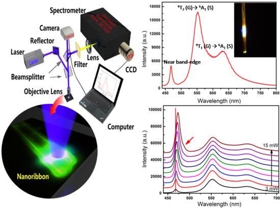
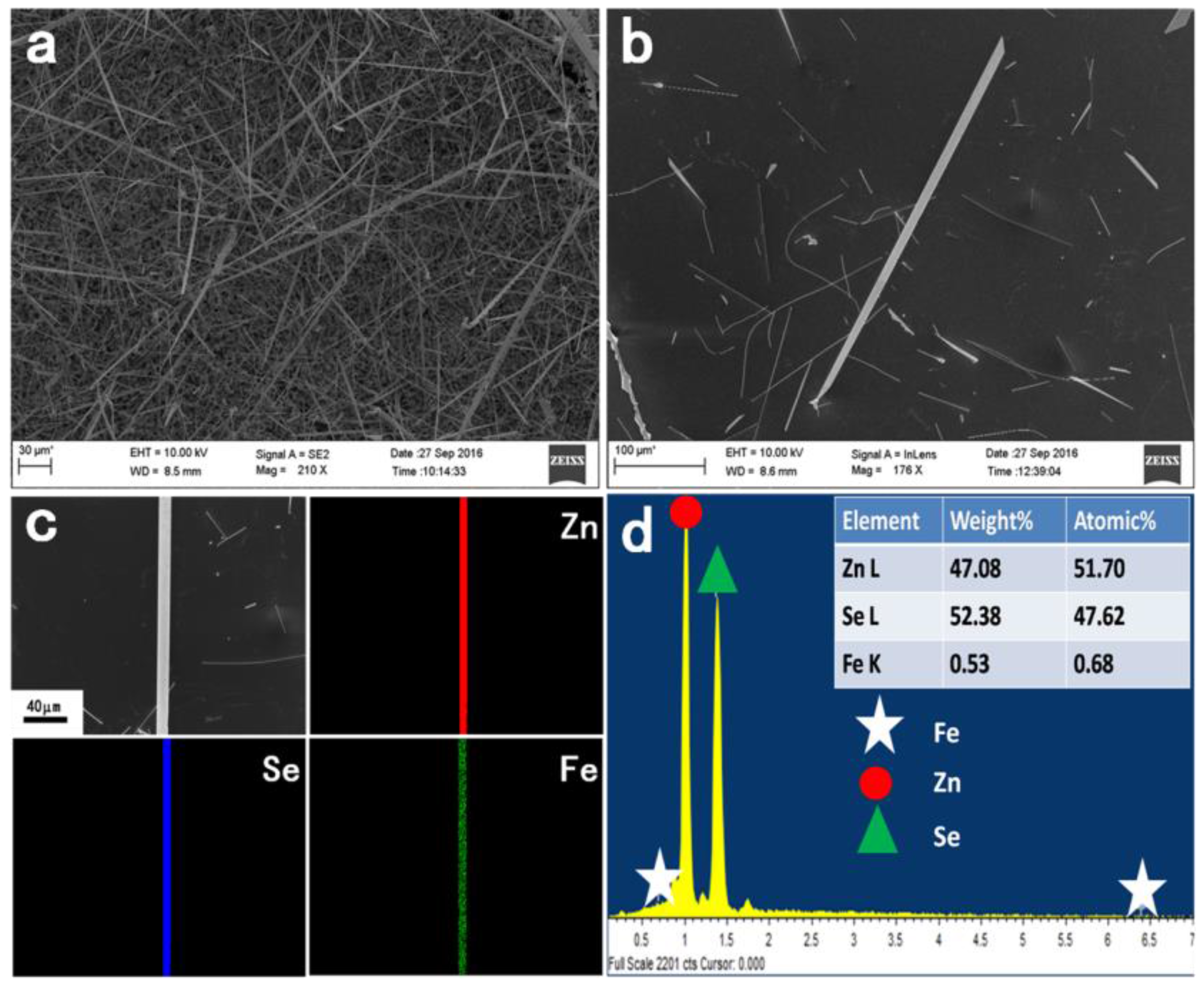
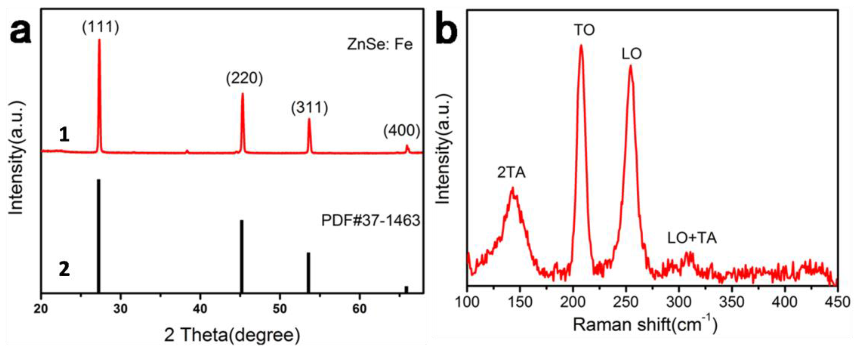
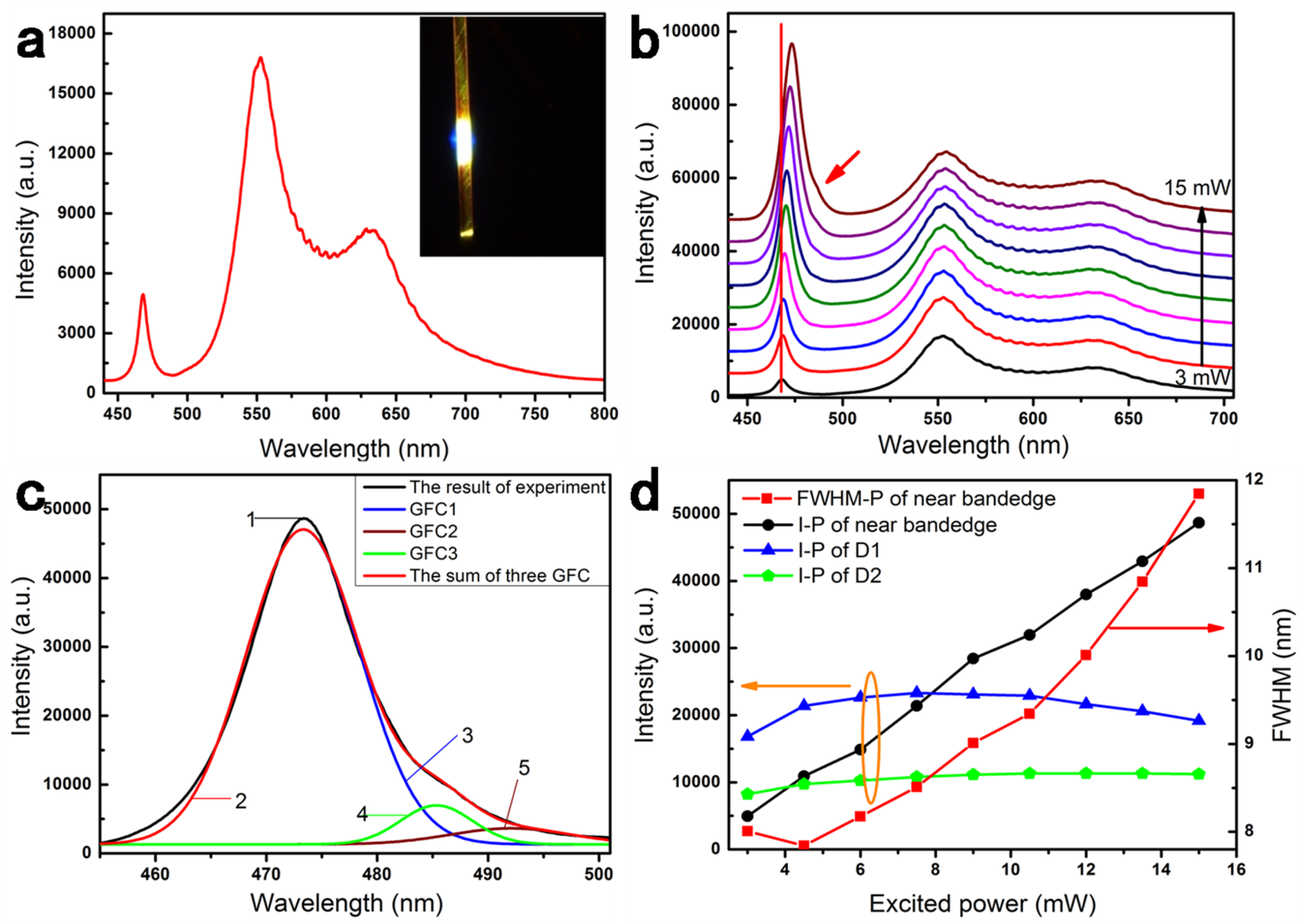
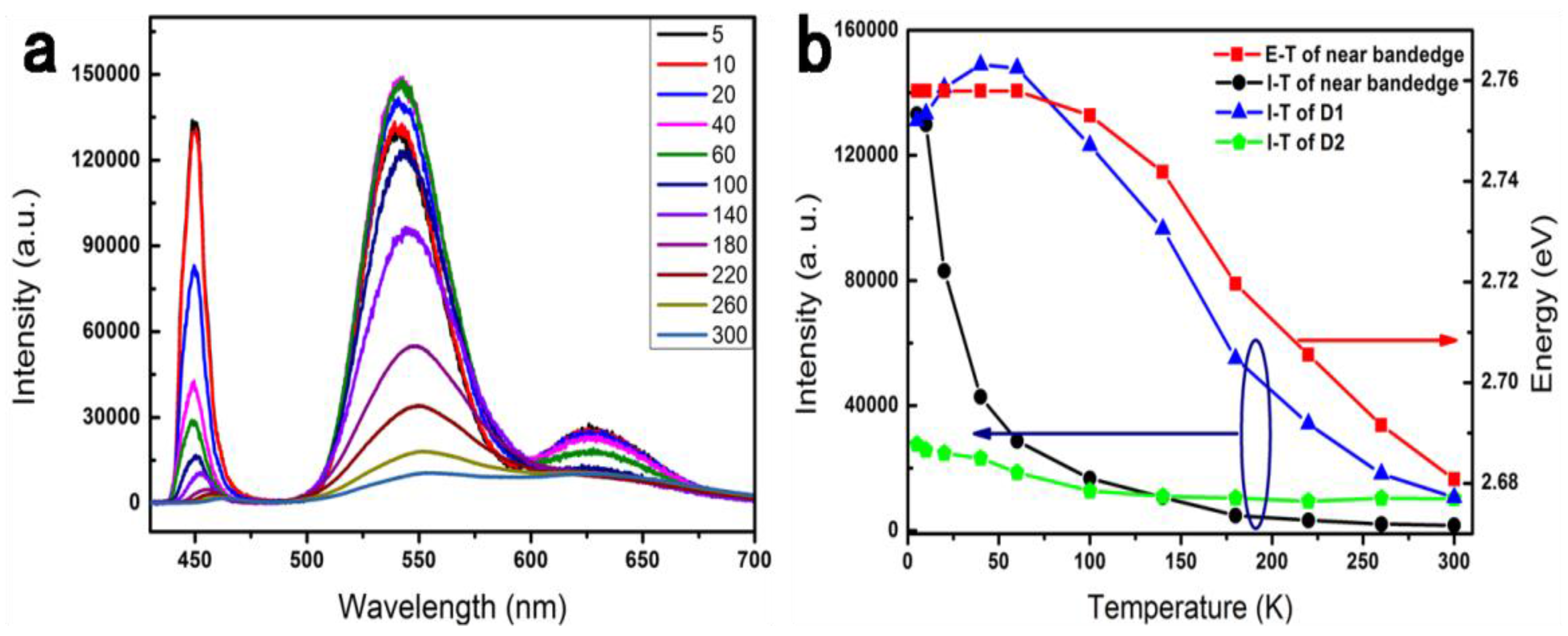
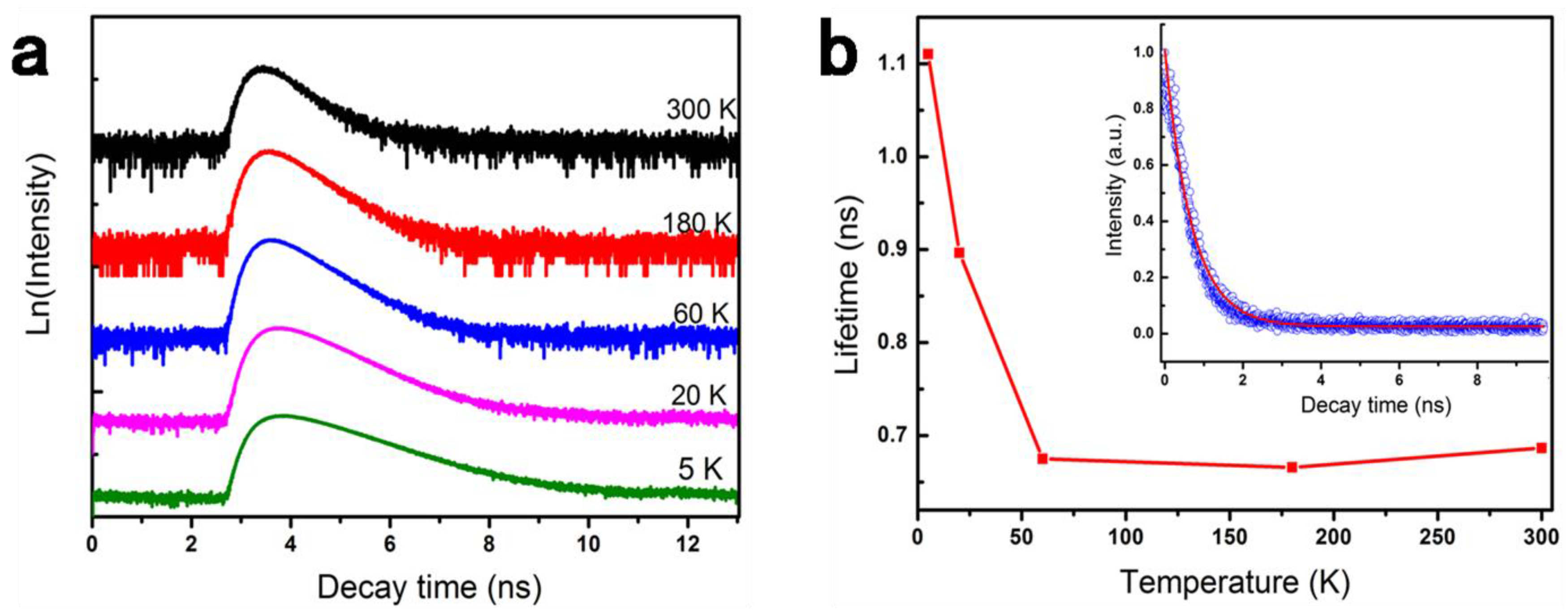
3. Results and Discussion

The morphology of as-synthesized Fe doped ZnSe nanoribbons is shown in Figure 1a. The nanoribbons are obtained in a large yield with a length of about 100–200 μm and a width of about 10 μm. Figure 1b shows an SEM image of an individual Fe doped ZnSe nanoribbon. Noticeably, the surface of the nanoribbon is clean and smooth. To confirm their elemental composition, EDS and EDS elemental mapping have been carried out. Figure 1c,d confirm the presence of three elements—Zn, Se, and Fe—illustrating that Fe ions are successfully doped into ZnSe nanoribbon relatively uniformly with an Fe atomic percent of about 0.68%.
Figure 2 shows an XRD pattern and micro-Raman spectrum of Fe doped ZnSe nanoribbons. The red curve in Figure 2a is an XRD pattern of as-synthesized Fe doped ZnSe nanoribbons, in which all of the diffraction peaks are in good agreement with standard values as listed in the Joint Committee on Powder Diffraction Standards (JCPDS) card of No. 37-1463 shown by the black line of Figure 2a. Specifically, the peak at 38° is attributed to the diffraction peak of wurtzite ZnSe, which might come from some ZnSe particles on the themica substrate. The strong diffraction peaks of the XRD pattern illustrate that the synthesized ZnSe nanoribbons are a zinc-blend structure and grow alone in the (111) crystal faces. Low concentration of Fe content leads to no other impurity or the secondary phase, as shown in the inset of Figure 1d and Figure 2a. Figure 2b shows the micro-Raman spectrum of an individual Fe doped ZnSe nanoribbon at room temperature measured by CW 532 nm laser exciting. The peaks at 143, 207, and 254 cm−1 correspond to the zinc-blend ZnSe two transverse acoustic (2TA) phonon modes [24], transverse optical (TO) phonon modes, and longitudinal optical (LO) phonon modes [25], respectively. The peak at 308 cm−1 is assigned to the superposition of LO and TA phonon modes, which is related to the defect state in the ZnSe lattice [26]. The strong and sharp peaks in the Raman spectrum demonstrate the crystalline nature of Fe doped ZnSe nanoribbons well.
In order to study the elementary excitations of Fe doped ZnSe nanoribbon, excited power-dependent PL spectra for one nanoribbon have been measured. Figure 3a shows its PL spectrum and optical morphology image of the nanoribbon in a dark field by 405 nm laser exciting. When a laser excites the nanoribbon, their endpoints emit yellow light, demonstrating that it has excellent optical waveguide properties, as shown in the inset of Figure 3a. In its PL spectrum, there are three emission peaks at 467, 553 and 630 nm, respectively. The first emission peak at 467 nm is assigned to near band-edge exciton emissions, whose nature needs further identification for the bandgap of pure ZnSe material is at about 2.7 eV (460 nm) at room temperature [27]. The second (D1) and third (D2) emission peak at 553 and 630 nm are related to Fe3+ d-d transition, which will be discussed later. Figure 3b shows power-dependent PL spectra from 3 to 15 mW, in which the emission peak of near band edge shifts to long wavelengths with excited power increasing. To study the origin and the redshift of near band-edge emission, the emission fitting curves have been obtained, as shown in Figure 3c. The black curve is the experimental line measured at P = 15 mW, which can be fitted by three Gaussian functions, denoted as GFC1 (473 nm), GFC2 (485 nm), and GFC3 (492 nm), respectively. The peak GFC1 originates from the bound exciton (BX) instead of the free exciton (FX) because it has lower energy than free excitons, and it can be confirmed later. The peak GFC3 should be attributed to the electron hole plasma (EHP) recombination emission, which has large full widths at half maximum (FWHM) and lower energy emission. At high power, higher carrier density is generated, which enhances carrier exchange interaction and leads to the band-gap renormalization of the nanoribbon [28], that is, it forms EHP recombination emission at high excited power and results in a red-shift of the emission peak [29]. This phenomenon is related to the photoheating by a CW laser. The GFC2 should be assigned to the emission of exciton magnetic polaron (EMP) due to the existence of ferromagnetic coupled Fe(III) cluster. At low excited power, the EMP emission in alio-valence ion doping ZnSe is not present, as shown in Figure 3b. The main elementary excitation of the near band-edge emission is bound excitons, and the EMP emission might be minor and merge with BX, so that EMP cannot be distinguished clearly. EMP can be enhanced at high excitation power due to larger binding energy, so a shoulder shows up at the long wavelength side of the near band-edge emission band (BX) at increasing powers. With further increasing power, a part of BX may dissociate into electron and hole to lead e-h plasma emission at around 493 nm due to excess charge effect of Fe3+, while EMP emission become significant in nanoribbons, as marked by the red arrow in Figure 3b. In addition, the energy span of GFC1 and GFC2 is 64 meV, which is larger than the energy of LO phonons, which eliminates the possibility of LO phonon replicas [3]. Previous works studied the formation and emission of EMP in transition metal ion doped II–VI semiconductor belts, which demonstrates EMP emission at the long wavelength side of FX. For example, Zou et al. researched the EMP behavior in Co doped CdS nanowires [30] and Liu et al. reported Mn doped ZnSe nanowires [31]. Thus, the GFC2 could be assigned to the EMP emission. With increasing powers, the FWHM of near band-edge emission band BX increases super-linearly, as shown with the red curve of Figure 3d, which is often related to the giant spin splitting of exciton states in TM doped semiconductors [32]. Moreover, their intensity increases linearly, as shown with the black line in Figure 3d, which confirms that it is TM ion dopant related BX and not only EMP that dominate the luminescence. The previous exciton state is related to the spin of a single TM ion dopant to couple with FX in the TM doped semiconductor, while EMP was the FX coupling with a multi-spin ferromagnetic coupled cluster in DMS. In both systems, the phonon scatterings are very involved in their relaxations. Then, some EHP recombination emissions become significant at high excitation power [33]. Due to the narrow measuring range, the intensity of the BX emission has not yet reached saturation, which also indicates a dominant component of BX in the near band-edge emission but not carriers.
The emission band D1 at 553 nm may be attributed to the internal 4T2 (G) → 6A1 (S) d-d transition of Fe3+ doped ZnSe, and the third band D2 may be related to the 4T1 (G) → 6A1 (S) of single Fe3+. Furthermore, Begum et al. have studied absorption spectrum of Fe3+ doped ZnSe nanoparticles, confirming the position of absorption peaks of 6A1 (S) → 4T2 (G) and 6A1 (S) → 4T1 (G) at 518 nm and 610 nm, respectively [23]. It is well known that free Fe3+ as Mn2+ has d5 configuration with parallel aligned spins (↑↑↑↑↑) in its ground state S according to Hund’s rule. If d-d transition can happen, it needs to flip at least one d spin to form the first excited state G (↑↑↑↑↓). In a Fe3+ doped ZnSe nanoribbon, the strong exchange interactions (p-d) between the extended p-band electrons of Se and the localized d electrons of Fe are responsible for the change of the forbidden transition (d-d transition), which also existed in FeSe-based superconductors [34]. Therefore, the D1 and D2 emission peaks are assigned to Fe3+ d-d transition. The emission of 6A1 (S) → 4T1 (G) is the lowest d-d transition, while 6A1 (S) → 4T2 (G) is the high-level transition. Usually, the lowest transition can only be detected. In fact, however, D2 is weaker than D1 in the intensity. Moreover, both of their energies shift to the low energy side (518 to 530 nm, and 610 to 630 nm), which clearly indicates that there is p-d hybridization inside. Another effect is the ferromagnetic coupling between neighboring Fe ions if Fe concentration is increased, which leads to a long-lifetime high d level and clear high level d-d transition. This phenomenon is often called “intra-shell emission” [30], as the strong emission at 553 nm.
It is easy to think that the emission peaks of D1 and D2 are related to structural defects of ZnSe nanoribbons. Many works reported the defect-related emissions between 500 and 700 nm, such as point defect Zn vacancies, Zn interstitials, and structure defects dislocations, stacking faults and so on [35,36,37]. In the PL spectrum of Fe3+ doped ZnSe nanoribbon, the narrow FWHM of D1 and D2 and the sharp near band-edge emission have eliminated the possibility of point defects for the latter often strongly relax the FX emission. The emission of structural defects is dependent on the change of temperatures. With this idea, temperature-dependent PL spectra are shown in Figure 4a. Figure 3d reveals that the intensities of the three emission peaks increase by increasing powers and the intensity of near band-edge emission increases faster than the emissions of D1 and D2 at the same time, indicating a clear character of a low defect lattice.
In Figure 4a, the near band-edge emission peak shifts from 450 nm (2.76 eV) to 463 nm (2.68 eV) with temperature increasing from 5 to 300 K, without peak splitting at low temperature. In Fe3+ ion doped ZnSe nanoribbons, Fe3+ ion substitutes for the Zn2+ site and introduces excess charges in ZnSe nanoribbons, resulting in the dominant BX and evanishing of EMP emission. Generally, the position of d-d transition emission of TM ions in a crystal does not shift with temperature changing, while they change with temperature in Fe3+ doped ZnSe nanostructure. This is because a high valence state Fe ion in a ZnSe lattice induces greater p-d hybridization, and introduces more phonon scattering effect. It then modifies the energy of D1 and D2 d-d emissions, as shown in Figure 4b. For heavy deep trap defects, this shift also scarcely happens. Hence, this phenomenon also demonstrates a difference from defect-related emission behavior [36]. The variation profiles of the emissions with temperatures increasing are plotted in Figure 4b. The energy variation trend of near band-edge emission with temperature is consistent with the Varshni function [38], as shown by the red line of Figure 4b. With increasing temperature, the intensities of near band-edge emission (black curve), D1 (blue curve), and D2 (green curve) emission decrease, which is due to the increasing of phonon scattering at high temperature and energy loss by thermal quenching [39]. The fast intensity reduction of near band-edge emission occurs because an exciton couples with an acoustic phonon and forms a bound exciton, which means that some Fe ions may be at the interstitial location. Interestingly, the intensity of the D1 emission peak increases firstly at low temperature (T < 50 K) and then starts to decrease with temperature increasing (T > 50 K). In the low temperature range, there is a thermal barrier or tunneling process that happens between the BX and the D1 state, which may be the valley potential well by Fe ions. There is another possibility coming from a ferromagnetic phase transition near 50 K, which needs further verification.
In order to study the dynamic process of BX in Fe(III) doped ZnSe nanoribbon, PL lifetime measurements have been carried out. Figure 5a shows temperature-dependent normalized PL lifetimes of near band-edge emission of an individual Fe doped ZnSe nanoribbon from 5 to 300 K. The lifetime of near band-edge emission decreases with increasing temperatures when the temperature is lower than 60 K, and then has a fluctuation at a little range when the temperature is beyond 60 K. The temperature-dependent PL lifetimes fitted by a single exponential function were plotted in Figure 5b. The inset of Figure 5b shows the fitted results of PL lifetimes at 300 K. With the temperature increasing, the lifetime decreases from 1.1 to 0.67 ns, which is mostly due to the strong coupling between exciton and acoustic phonons. In particular, the lifetime has a sharp reduction when the temperature lowers than 60 K, which is different from that previously reported [40]. The magnetic phase transition in Fe doped ZnSe nanoribbon may be one cause.

4. Conclusions

In summary, we synthesized high quality Fe3+ doped ZnSe nanoribbons by the CVD method, which is confirmed by SEM images, XRD patterns, micro-Raman spectrum and PL spectra. Micro-photoluminescence spectra of an individual Fe3+ doped ZnSe nanoribbon have been measured, which show three emission peaks: near bandedge emission peak at 467 nm and two Fe3+ d-d transition emission peaks at 553 nm (D1) and 630 nm (D2), respectively. The power-dependent PL spectra demonstrate that bound exciton emission in near band edge is dominated at low excited power, while it shows that EMP and EHP component emission characteristics with excited power increasing. The emission peak at 553 nm is assigned to 4T2 (G) → 6A1 (S) d-d transition and the peak at 630 nm to 4T1 (G) → 6A1 (S) of Fe3+, in which p-d hybridization plays an important role in the transition. Excited power-dependent PL spectra show that alio-valent doping has a great impact on the formation and emission of EMP in a diluted magnetic semiconductor. Temperature-dependent PL spectra further confirm the conclusions. Temperature-dependent lifetime measurements clarify the exciton and phonon interaction and show a break point in the curve of lifetime versus temperature, which may be related to a magnetic phase transition.

Acknowledgments

This work was supported by the National Natural Science Foundation of China (No. 11004009), the 973 Project of China (No. 2014CB920903), the Special Key Project for the National Strong Magnetic Field Center at Huazhong University of Science and Technology (HUST) (No. 2015KF03) and the Renovation Team Fund (BIT-2011).

Author Contributions

Lipeng Hou performed the experiment and wrote the paper; Cheng Chen participated in part of the experiment measurements; Li Zhang, Qiankun Xu, Xinxin Yang, and Muhammad Ismail Farooq revised the manuscript and participated in part of the experiment measurements; Junbo Han provided the facilities and discussed the results; Ruibin Liu, Yongyou Zhang and Lijie Shi participated in the discussions of the results; Bingsuo Zou supervised the work and led the discussions.

Conflicts of Interest

The authors declare no conflict of interest.

References

  1. Vukovic, N.; Healy, N.; Sparks, J.R.; Badding, J.V.; Horak, P.; Peacock, A.C. Tunable continuous wave emission via phase-matched second harmonic generation in a ZnSe microcylindrical resonator. Sci. Rep. 2015, 5, 11798. [Google Scholar] [CrossRef] [PubMed]
  2. Pawlis, A.; Panfilova, M.; As, D.; Lischka, K.; Sanaka, K.; Ladd, T.; Yamamoto, Y. Lasing of donor-bound excitons in ZnSe microdisks. Phys. Rev. B 2008, 77, 153304. [Google Scholar] [CrossRef]
  3. Hite, G.E.; Marple, D.T.F.; Aven, M.; Segall, B. Excitons and the absorption edge in ZnSe. Phys. Rev. 1967, 156, 850–859. [Google Scholar] [CrossRef]
  4. Ding, J.; Jeon, H.; Ishihara, T.; Hagerott, M.; Nurmikko, A.V.; Luo, H.; Samarth, N.; Furdyna, J. Excitonic gain and laser emission in ZnSe-based quantum wells. Phys. Rev. Lett. 1992, 69, 1707–1710. [Google Scholar] [CrossRef] [PubMed]
  5. Su, X.; Zheng, H. Influence of spin-phonon coupling on the spin-1/2 antiferromagnet on a square lattice. Solid State Commun. 1999, 109, 323–328. [Google Scholar] [CrossRef]
  6. Sangiovanni, G.; Gunnarsson, O.; Koch, E.; Castellani, C.; Capone, M. Electron-phonon interaction and antiferromagnetic correlations. Phys. Rev. Lett. 2006, 97, 046404. [Google Scholar] [CrossRef] [PubMed]
  7. Norris, D.J.; Yao, N.; Charnock, F.T.; Kennedy, T.A. High-quality manganese-doped ZnSe nanocrystals. Nano Lett. 2001, 1, 3–7. [Google Scholar] [CrossRef]
  8. Song, Y.; Sonntag, J.; Mirov, S.B.; Gmachl, C.F.; Khurgin, J.B. Mid-infrared light emission from a Fe2+: ZnSe polycrystal using quantum cascade laser pumping. Appl. Phys. Lett. 2014, 105, 141108. [Google Scholar] [CrossRef]
  9. Luo, M.; Giles, N.C.; Roy, U.N.; Cui, Y.; Burger, A. Energy transfer between Co2+ and Fe2+ ions in diffusion-doped ZnSe. J. Appl. Phys. 2005, 98, 083507. [Google Scholar] [CrossRef]
  10. Vlaskin, V.A.; Janssen, N.; van Rijssel, J.; Beaulac, R.M.; Gamelin, D.R. Tunable dual emission in doped semiconductor nanocrystals. Nano Lett. 2010, 10, 3670–3674. [Google Scholar] [CrossRef] [PubMed]
  11. Wang, C.; Xu, J.; Wang, Y.; Xu, S.; Qi, Z.; Lu, C.; Cui, Y. Manipulation of irradiative defects at MnSe and ZnSe dopant-host interface. Adv. Funct. Mater. 2016, 26, 4274–4282. [Google Scholar] [CrossRef]
  12. Kulyuk, L.L.; Laiho, R.; Lashkul, A.V.; Lähderanta, E.; Nedeoglo, D.D.; Nedeoglo, N.D.; Radevici, I.V.; Siminel, A.V.; Sirkeli, V.P.; Sushkevich, K.D. Magnetic and luminescent properties of iron-doped ZnSe crystals. Phys. B 2010, 405, 4330–4334. [Google Scholar] [CrossRef]
  13. Zhang, X.; Zhang, X.; Wang, L.; Wu, Y.; Wang, Y.; Gao, P.; Han, Y.; Jie, J. ZnSe nanowire/Si p-n heterojunctions: Device construction and optoelectronic applications. Nanotechnology 2013, 24, 395201. [Google Scholar] [CrossRef] [PubMed]
  14. Zhou, J.; Li, Y.; Wu, X.; Qin, W. Modulating the electronic and optical properties of tetragonal ZnSe monolayers by chalcogen dopants. ChemPhysChem 2016, 17, 1993–1998. [Google Scholar] [CrossRef] [PubMed]
  15. Binh, P.H.; Hung, N.T. High-speed visible light communications using ZnSe-based white light emitting diode. IEEE Photonics Technol. Lett. 2016, 28, 1948–1951. [Google Scholar] [CrossRef]
  16. Dietl, T. A ten-year perspective on dilute magnetic semiconductors and oxides. Nat. Mater. 2010, 9, 965–974. [Google Scholar] [CrossRef] [PubMed]
  17. Walsh, A.; Da Silva, J.; Wei, S.H. Theoretical description of carrier mediated magnetism in cobalt doped ZnO. Phys. Rev. Lett. 2008, 100, 256401. [Google Scholar] [CrossRef] [PubMed]
  18. Dietl, T.; Ohno, H. Dilute ferromagnetic semiconductors: Physics and spintronic structures. Rev. Mod. Phys. 2014, 86, 187–251. [Google Scholar] [CrossRef]
  19. Wu, M.W.; Jiang, J.H.; Weng, M.Q. Spin dynamics in semiconductors. Phys. Rep. 2010, 493, 61–236. [Google Scholar] [CrossRef]
  20. Kamran, M.A.; Liu, R.; Shi, L.J.; Li, Z.A.; Marzi, T.; Schoppner, C.; Farle, M.; Zou, B. Tunable emission properties by ferromagnetic coupling Mn(II) aggregates in Mn-doped CdS microbelts/nanowires. Nanotechnology 2014, 25, 385201. [Google Scholar] [CrossRef] [PubMed]
  21. Heitz, R.; Hoffmann, A.; Broser, I. Fe3+ center in ZnO. Phys. Rev. B 1992, 45, 8977–8988. [Google Scholar] [CrossRef]
  22. Furdyna, J.K. Diluted magnetic semiconductors. J. Appl. Phys. 1988, 64, R29–R64. [Google Scholar] [CrossRef]
  23. Begum, S.M.; Rao, M.C.; Aparna, Y.; Rao, P.S.; Ravikumar, R.V. Spectroscopic investigations of Fe3+ doped poly vinyl alcohol (PVA) capped ZnSe nanoparticles. Spectrochim. Acta Part A 2012, 98, 100–104. [Google Scholar] [CrossRef] [PubMed]
  24. Yadav, K.; Jaggi, N. Aging effect on the structural and optical properties of ZnSe nanostructures. J. Mater. Sci. Mater. Electron. 2015, 27, 393–398. [Google Scholar] [CrossRef]
  25. Anand, S.; Verma, P.; Jain, K.P.; Abbi, S.C. Temperature dependence of optical phonon lifetimes in ZnSe. Phys. B 1996, 226, 331–337. [Google Scholar] [CrossRef]
  26. Wang, F.; Zhang, Z.; Liu, R.; Wang, X.; Zhu, X.; Pan, A.; Zou, B. Structure and stimulated emission of ZnSe nanoribbons grown by thermal evaporation. Nanotechnology 2007, 18, 305705. [Google Scholar] [CrossRef]
  27. Xing, G.; Luo, J.; Li, H.; Wu, B.; Liu, X.; Huan, C.H.A.; Fan, H.J.; Sum, T.C. Ultrafast exciton dynamics and two-photon pumped lasing from ZnSe nanowires. Adv. Opt. Mater. 2013, 1, 319–326. [Google Scholar] [CrossRef]
  28. Ugeda, M.M.; Bradley, A.J.; Shi, S.F.; Felipe, H.; Zhang, Y.; Qiu, D.Y.; Ruan, W.; Mo, S.K.; Hussain, Z.; Shen, Z.X.; et al. Giant bandgap renormalization and excitonic effects in a monolayer transition metal dichalcogenide semiconductor. Nat. Mater. 2014, 13, 1091–1095. [Google Scholar] [CrossRef] [PubMed]
  29. Bagnall, D.M.; Chen, Y.F.; Zhu, Z.; Yao, T.; Shen, M.Y.; Goto, T. High temperature excitonic stimulated emission from ZnO epitaxial layers. Appl. Phys. Lett. 1998, 73, 1038–1040. [Google Scholar] [CrossRef]
  30. Zou, S.; Kamran, M.A.; Shi, L.J.; Liu, R.; Guo, S.; Kavokin, A.; Zou, B. Bosonic lasing from collective exciton magnetic polarons in diluted magnetic nanowires and nanobelts. ACS Photonics 2016, 3, 1809–1817. [Google Scholar] [CrossRef]
  31. Liu, R.; Shi, L.; Zou, B. The magnetic exciton relaxation and spin-spin interaction by the time-delayed photoluminescence spectra of ZnO: Mn nanowires. ACS Appl. Mater. Interfaces 2014, 6, 10353–10366. [Google Scholar] [CrossRef] [PubMed]
  32. Komarov, A.V.; Ryabchenko, S.M.; Terletseii, O.V. Giant spin splitting of exciton states in ZnSe with Mn and Fe impurities. Phys. Status Solidi b 1980, 102, 603–609. [Google Scholar] [CrossRef]
  33. Zu, P.; Tang, Z.K.; Wong, G.K.L.; Kawasaki, M.; Ohtomo, A.; Koinuma, H.; Segawa, Y. Ultraviolet spontaneous and stimulated emissions from ZnO microcrystallite thin films at room temperature. Solid State Commun. 1997, 103, 459–463. [Google Scholar] [CrossRef]
  34. Lu, X.F.; Wang, N.Z.; Wu, H.; Wu, Y.P.; Zhao, D.; Zeng, X.Z.; Luo, X.G.; Wu, T.; Bao, W.; Zhang, G.H.; et al. Coexistence of superconductivity and antiferromagnetism in (Li0.8Fe0.2)OHFeSe. Nat. Mater. 2015, 14, 325–329. [Google Scholar] [CrossRef] [PubMed]
  35. Zhang, X.T.; Liu, Z.; Leung, Y.P.; Li, Q.; Hark, S.K. Growth and luminescence of zinc-blende-structured ZnSe nanowires by metal-organic chemical vapor deposition. Appl. Phys. Lett. 2003, 83, 5533. [Google Scholar] [CrossRef]
  36. Zou, Y.; Li, H.; Ren, P.; Xu, J.; Ma, L.; Wang, X.; Fan, X.; Shan, Z.; Zhuang, X.; Zhou, H.; et al. Microphotoluminescence of individual ZnSe nanoribbons. Mater. Lett. 2014, 129, 118–121. [Google Scholar] [CrossRef]
  37. Philipose, U.; Xu, T.; Yang, S.; Sun, P.; Ruda, H.E.; Wang, Y.Q.; Kavanagh, K.L. Enhancement of band edge luminescence in ZnSe nanowires. J. Appl. Phys. 2006, 100, 084316. [Google Scholar] [CrossRef]
  38. Malikova, L.; Krystek, W.; Pollak, F.H.; Dai, N.; Cavus, A.; Tamargo, M.C. Temperature dependence of the direct gaps of ZnSe and Zn0.56Cd0.44Se. Phys. Rev. B 1996, 54, 1819–1824. [Google Scholar] [CrossRef]
  39. He, H.; Yang, Q.; Liu, C.; Sun, L.; Ye, Z. Size-dependent surface effects on the photoluminescence in ZnO nanorods. J. Phys. Chem. C 2010, 115, 58–64. [Google Scholar] [CrossRef]
  40. Yang, G.; Ma, Z.; Zhong, H.; Zou, S.; Chen, C.; Han, J.; Zou, B. Probing exciton move and localization in solution-grown colloidal CdSexS1–x alloyed nanowires by temperature- and time-resolved spectroscopy. J. Phys. Chem. C 2015, 119, 22709–22717. [Google Scholar] [CrossRef]
Figure 1. (a) Scanning electron microscopy (SEM) image of as-prepared Fe doped ZnSe nanoribbons; (b) SEM image of an individual Fe doped ZnSe nanoribbon; (c) Energy dispersive spectroscopy (EDS) elemental mapping of detecting three elements Zn, Se, and Fe, respectively; and the (d) EDS profile of a point of Fe doped ZnSe nanoribbon of (c). The inset is elemental content of the three elements of Fe doped ZnSe nanoribbon.
Applsci 07 00039 g001
Figure 2. (a) X-ray diffractometer (XRD) pattern of as-prepared Fe doped ZnSe nanoribbons. The corresponding Miller indexes are labeled at the top of the diffraction peaks. The red line 1 is the experimental results of the Fe doped ZnSe nanoribbon, and the black line 2 is the Joint Committee on Powder Diffraction Standards (JCPDS) card of No. 37-1463 of pure ZnSe material; and (b) the micro-Raman spectrum of an individual Fe doped ZnSe nanoribbon with a continuous wave (CW) 532 nm laser as the excited source at room temperature.
Applsci 07 00039 g002
Figure 3. (a) The photoluminescence (PL) spectrum of an individual Fe doped ZnSe nanoribbon with a 405 nm laser at excitation power P = 3 mW. The inset in the top right corner is the PL image of the nanoribbon in the dark field observation; (b) the power-dependent PL spectra of an individual Fe doped ZnSe nanoribbon at room temperature. The black arrow represents the increasing direction of excitation power; (c) fitting result of near band-edge emission band by Gaussian functions at excitation power P = 15 mW. The black curve 1 is experimental data; the blue 3, green 4 and brown 5 represent three fitting lines of Gaussian function curve (GFC)1, GFC2, and GFC3, respectively; and the red line 2 is the superposition of the three above GFCs; (d) Full widths at half maximum (FWHM) of near band-edge emission band changing with excitation power (filled square, red). Plot of intensity (I) versus excitation power (P) for near band edge (filled circles, black, 467 nm), D1 (filled triangles, blue, 553 nm), and D2 (filled pentagons, green, 630 nm) emission peaks.
Applsci 07 00039 g003
Figure 4. (a) temperature-dependent PL spectra of an individual Fe doped ZnSe nanoribbon from 5 to 300 K with 405 nm laser excitation; (b) the variation curves of intensity (I) (filled circles, filled triangles, and filled pentagons) and energy (E) (filled square) of emission peaks as a function of temperatures (T). The filled square shows the relationship between energy and temperature of near band edge and the filled circles, triangles, and pentagons curves correspond to intensity versus temperature of near band edge, D1 (filled triangles, 553 nm), and D2 (filled pentagons, 630 nm) emission peaks, respectively.
Applsci 07 00039 g004
Figure 5. (a) temperature-dependent normalized PL lifetime measurement of near band-edge emission of an individual Fe doped ZnSe nanoribbon from 5 to 300 K with 405 nm femtosecond pulsed laser (duration: ~130 fs, repetition rate: 76 MHz) as the excitation source; (b) plot of lifetime versus temperature. The inset is normalization PL lifetime decay curve (circles curve) at 300 K and its fitted curve (solid line) by single exponential function.
Applsci 07 00039 g005

