Article

Design and Realization of a Frequency Reconfigurable Multimode Antenna for ISM, 5G-Sub-6-GHz, and S-Band Applications

1
Department of Electrical and Electronic Engineering, Auckland University of Technology, Auckland 1010, New Zealand
2
Department of Integrated IT Engineering, Seoul National University of Science and Technology, Seoul 01811, Korea
3
Telecommunication Engineering Department, University of Engineering Technology, Taxila 47050, Pakistan
4
Department of Computer and Communication Engineering, Chungbuk National University, Chungbuk 28644, Korea
5
Electronic Engineering Department, University of Rome “Tor Vergata”, Via del Politecnico 1, 00133 Rome, Italy
6
Electric, Electronic and Communication Engineering Department, Public University of Navarre, 31006 Pamplona, Spain
7
Institute of Smart Cities, Public University of Navarre, 31006 Pamplona, Spain
*
Authors to whom correspondence should be addressed.
Appl. Sci. 2021, 11(4), 1635; https://doi.org/10.3390/app11041635
Submission received: 19 January 2021 / Revised: 8 February 2021 / Accepted: 8 February 2021 / Published: 11 February 2021
(This article belongs to the Special Issue Millimeter-wave and Terahertz Applications of Metamaterials)

Abstract

:
This paper presents the design and realization of a compact size multimode frequency reconfigurable antenna. The antenna consists of a triangular-shaped monopole radiator, originally inspired from a rectangular monopole antenna. Slots were utilized to notch the desired frequency while the PIN diodes were utilized to achieve frequency reconfigurability. The antenna can operate in wideband, dual-band, or tri-band mode depending upon the state of the diodes. To validate the simulation results, a prototype was fabricated, and various performance parameters were measured and compared with simulated results. The strong agreement between simulated and measured results along with superior performance as compared to existing works in the literature makes the proposed antenna a strong candidate for ISM, 5G-sub-6 GHz, and S-band applications.

1. Introduction

Multifunctional antennas have gained considerable attention in the past decade due to advanced level technologies like 5G, Internet of Things (IoT), etc., along with a need for compact devices. The reconfigurable antennas are well-known due to the numerous advantages. These antennas can replace multiple antennas by showing switching frequency, polarization, and radiation patterns using various techniques [1,2]. The RF-PIN diodes, Micro Electrical and Mechanical Switches (MEMS), Optical switch, microfluids, meta-surface, and electrically phase change materials are widely used to achieve the of reconfigurability [3,4]. Among various types of antennas proposed for sub-6-GHz applications, most of the reported works are related to reconfigurable antennas where RF-PIN diode for frequency reconfigurability was widely studied by the researchers to achieve single band, dual-band, and multiple-band reconfigurable operations [5,6,7,8,9,10,11,12,13,14,15,16,17].
In [5], a wideband antenna was designed for Wireless Wide Area Network (WWAN) and Long-Term Evolution (LTE) applications. The antenna comprises of simple structure that shows good performance over a wide operational band. However, the antenna suffers from several drawbacks, including a bigger dimension, low gain, and it did not support reconfigurability. In [6], a compact wideband monopole antenna is converted into tri-band antenna for ISM and 5G-sub-6-GHz applications. Although the antenna offers a compact size with the advantages of flexibility, it does not support frequency reconfiguration. Similarly another antenna by using the proximity-coupling feed to cover the WLAN and 5G-sub-6-GHz was presented in [7]. However, the proposed antenna has complex antenna structure that is the combination of two substrate separated by air gap. Several single band frequency reconfigurable antennas are proposed to operate in frequency band spectrum ranges 2–4.5 GHz [8,9,10,11,12]. Although the antennas reported in [8,9,10] are offering very high gain characteristics, they have multiple layered structures, which resulted in increased thickness and structural complexity. Although the work reported antennas in [11,12] offer compact size, they cover very limited bandwidth, making them not suitable for modern-day devices operates in wideband frequency spectrums.
Antennas with frequency reconfigurable characteristics for LTE and Wireless Local Area Network (WLAN) applications are presented in [13,14]. A conventional rectangular patch antenna was modified by using Defected Ground Structure (DGS) for wideband operation, and three PIN diodes were incorporate to switch the operation [13]. In [14], various slots and asymmetric feed is utilized along with two pin diodes, to achieve frequency reconfigurability. Although these antennas have compact and simple geometry, the operational bandwidth in single and dual band is narrow. A dual to tri-band and a dual-band to quad-band frequency reconfigurable antenna were presented in [15,16], respectively. Although, these antenna designs cover many bands, however, both works have impediment of narrow bandwidth, complex geometrical structures and lesser number of operational modes. In addition, the antenna presented in [15] suffers from the draw back of larger dimensions. A flexible frequency reconfigurable antenna was presented in [17] for sub-6-GHz applications. The presented work offers wideband and two dual-band operational modes with relatively simple structure. However, it has larger dimensions and limited operational bandwidth.
To overcome the aforementioned challenges, a compact frequency reconfigurable antenna is proposed in this paper. The antenna radiator is composed of a triangular radiator with V-shaped slots and two PIN diodes are utilized to achieve frequency reconfigurability. The presented work shows a good combination of compact size, multimode operation, simple geometrical configuration, wide operational region, and reasonable gain. The rest of the paper is organized as follows. Section 2 presents the theoretical analysis and design methodology of the proposed antenna. Section 3 illustrates the discussion on various performance parameters of the presented work, while the paper is concluded in Section 4.

2. Materials and Methods

2.1. Antenna Geometry

The geometrical configuration of the proposed antenna is illustrated in Figure 1. The antenna is designed using ROGERS RT/droid 6010 having dielectric loss tangent (tan δ) of 0.0023, relative permittivity (εr) of 10.2 and 1.9-mm thickness (H) [18]. The overall dimension of the reconfigurable antenna is AX × AY. It can be seen from Figure 1a that the proposed monopole antenna consists of a triangle-shaped radiator having a dimension of PX × PY and the feed line dimension is FX × FY. Two V-shaped slots were etched to notch the desire bands from wide bandwidth, the total length of the long slot is 2 × L1, whereas the length of the shorter slot is 2 × L2. The width of both slots had a dimension of d while the gap between two slots is g. A truncated ground plane of length GX was used to achieve wideband operational bandwidth. Table 1 shows the optimized parameters of the antenna.

2.2. Simulation Setup

The simulations of the proposed frequency reconfigurable antenna were performed using Higher Frequency Structural Simulator (HFSS). For frequency reconfigurability two RF PIN diodes D1 and D2 (Infineon, model # BAR50-02) were utilized. Two capacitors C1 and C2 were used to connect the pads with the radiator physically and to block current flow from biasing pads to the radiator. Capacitor CDC is utilized to stop the flow of current toward the connector which may affect the performance of the antenna. The pads for diode are connected using a vias to biasing pads presented at the backside of the antenna, as depicted in Figure 1b. Inductor I is employed to stop the unwanted RF-current from the source VDC. The biasing voltage is provided from the backside of the antenna to mitigate the effects of DC-wires on the performance of the antenna.

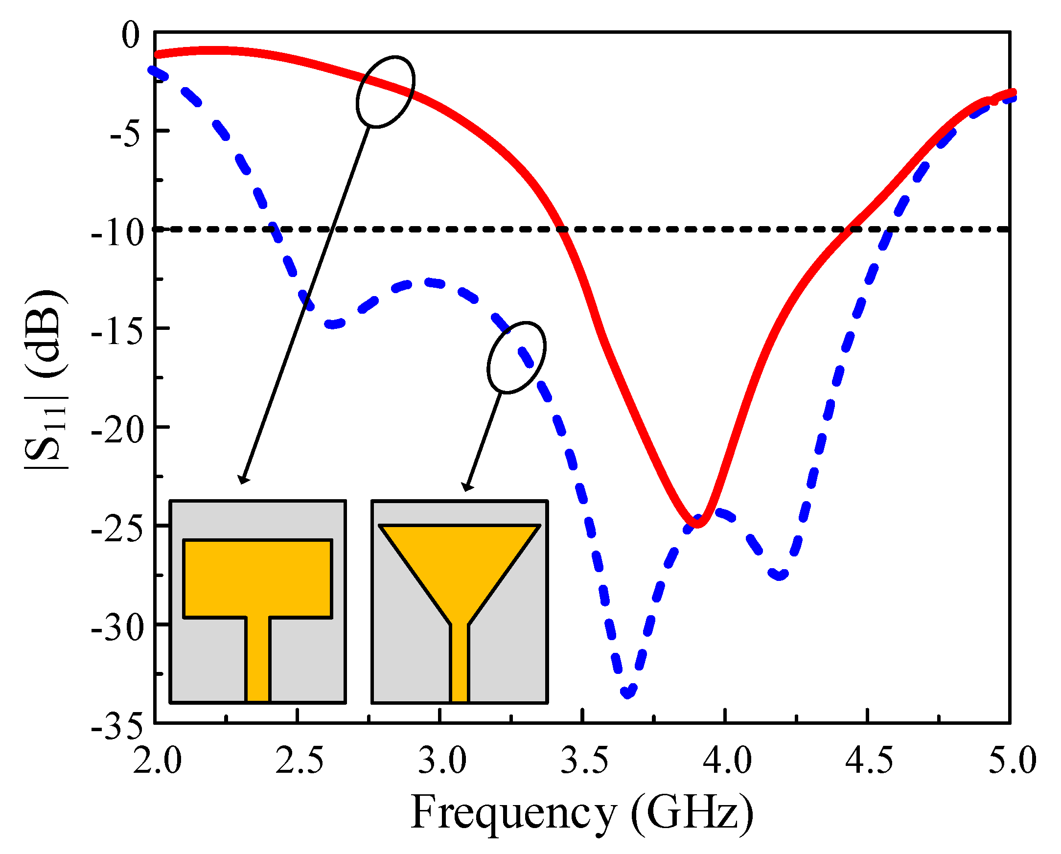
2.3. Design of Wideband Antenna

The proposed reconfigurable antenna was originally inspired by a conventional quarter-wave rectangular monopole antenna, and the basic concept of the proposed antenna and designed methodology was already presented in [19]. The length (LR) of the rectangular monopole antenna could be estimated by using the following equation provided in [20]:
L R = C o 4 f c ε e f f
where Co represents the speed of light in free space, fc represents the central frequency; for the presented case it was selected to be 4 GHz, whereas, εeff is the effective dielectric constant of the substrate is calculated by using the following relation:
ε e f f ε r + 1 2 + ε r 1 2   { ( 1 + 12 A Y H ) 0.5 }
where H is the thickness of the substrate, and AY is the width of the substrate.
The resultant antenna resonates at 3.8 GHz with an impedance bandwidth of 850-MHz ranging 3.55–4.4 GHz, as depicted in Figure 2. Although the antenna offers a wide impedance bandwidth, still it does not cover the targeted 5G sub-6-GHz band (3.1–4.5 GHz) allocated globally for future wireless communications. Thus, perturbation techniques were utilized to widen the impedance bandwidth of the antenna. Different from common techniques including DGS and slots to achieve wideband behavior, this design employed truncation of radiator corners to improve the bandwidth. Both lower corners were truncated using an equilateral triangle which results in increasing the effective length of the radiator, thus shifting of resonance toward the lower frequencies, as depicted in Figure 2. Moreover, truncation of the corner causes more current to flow from the feedline to the radiator. Due to the triangular shape, the current uniformly distribute itself on the surface of the radiator. The increase in flow and uniform distribution of current resulted in improvement in impedance matching at lower frequencies to enhances the impedance bandwidth of the antenna. The resultant antenna exhibits a wide impedance bandwidth of 2.2 GHz ranging 2.35–4.55 GHz which corresponds to 62.8% of central frequency, as depicted in Figure 2. It is worthy to note here that besides 5G sub-6-GHz band spectrum the antenna also covers 2.4 GHz WLAN band, 2.45 GHz ISM band, 2.5GHz Wi-Max band, and more than 90% of S-band (2–4 GHz), thus making it suitable for multiple applications.

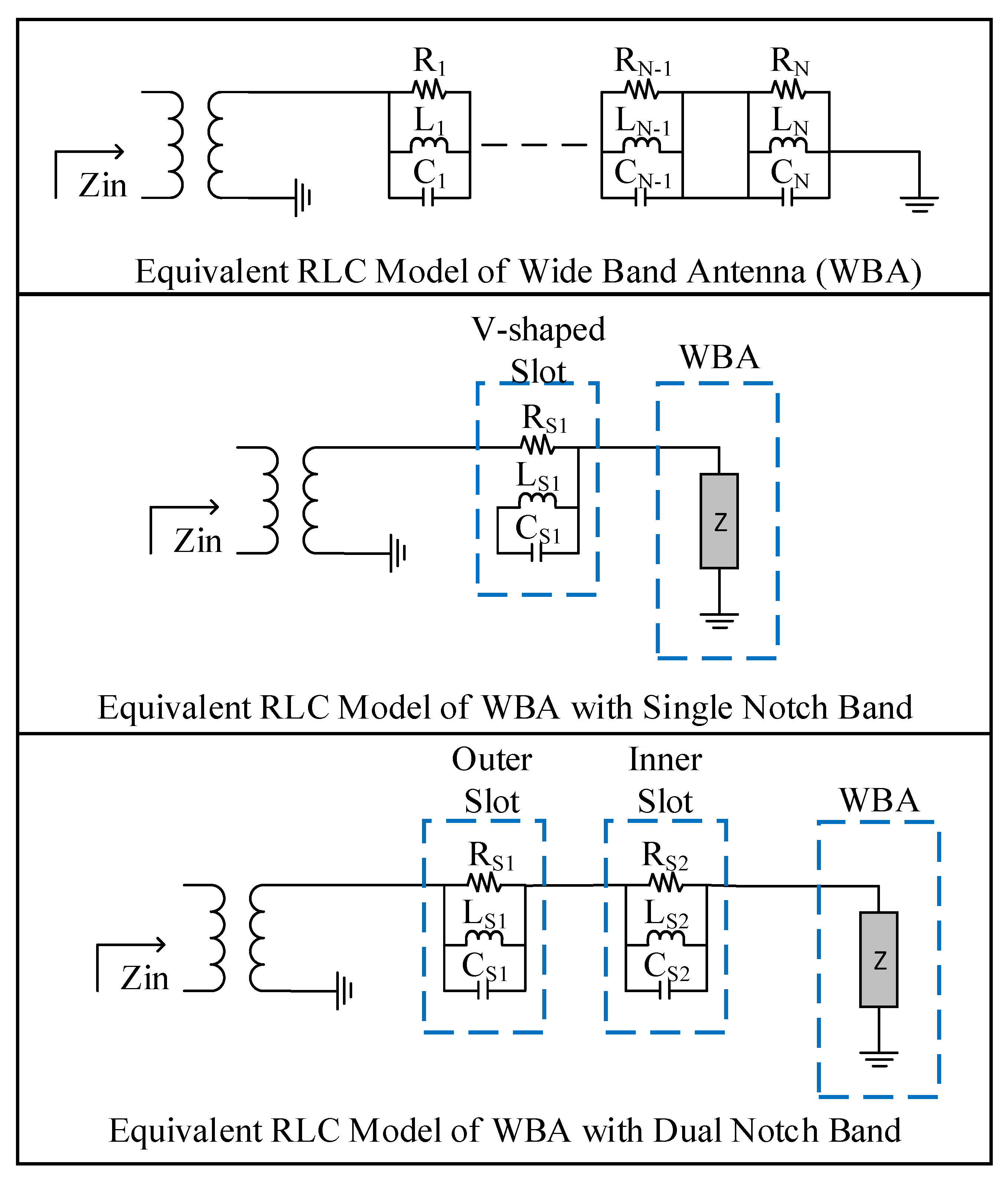
2.4. Design of Notch Band Antenna

To overcome the problem of band congestion due to the closely allocated band spectrums for various applications, the wideband antenna designed in the previous section is transformed into a notch band antenna. Usage of additional filters is the common way to notch the desire bands [21]. However, it may result in various drawbacks, including the requirement of additional matching circuits to match the impedance of the filter with wideband antenna [22]. Furthermore, it also requires a bigger area to fit the whole circuit allowing very little space for other components thus limits its usage in compact size devices [23]. Therefore, the researcher adopted various techniques including etching slots [24], loading metamaterials [25], insertion of Split Ring Resonator (SSR) [26], and stub loading techniques [27] to notch the desire bands.
Furthermore, to avoid complex geometrical configuration, a simple yet effective technique to achieve a notched band is adopted, i.e., etching the slot in the radiator. One of the key parameters is to select the shape and position to place the slot, therefore, the shape and position of the slot must be chosen carefully to achieve a high value of VSWR to minimize the interference of the notch bands [28]. For the said purpose two V-shaped slots were used to achieve dual notch bands, the effective length (LS) of the slot for desire frequency (fd) can be calculated by [29]:
L S ( n ) = C o 2 f d ( n ) ε e f f
where (n) = 1, 2 which shows the number of slot while ε e f f ( ε r + 1 ) 2 . Moreover, for the proposed work LS1 = 2 × L1 while LS2 = 2 × L2. Figure 3 illustrates the comparison between simulated values of S11 for wideband antenna and antenna with a single and dual notch. It could be observed that with a single V-shaped slot the antenna mitigates the band spectrum of 2.47–3.11 GHz having a maximum value of S11 = −0.78 dB at 2.82 GHz. Similarly, when two slots were etched, the antenna mitigates the two band spectrums of 2.48–2.96 GHz and 3.47–3.76 GHz. To have a better understanding of the slot to mitigate the desired frequency, current distribution plots were presented in Figure 4a,b. It could be observed from Figure 4a that for the first notch band the maximum current is around the bigger V-shaped slots, which causes the mitigation of the lower band. Similarly, the maximum current was observed along with a smaller V-shaped slot for the second notch band, which causes its mitigation from the resonating band spectrum.

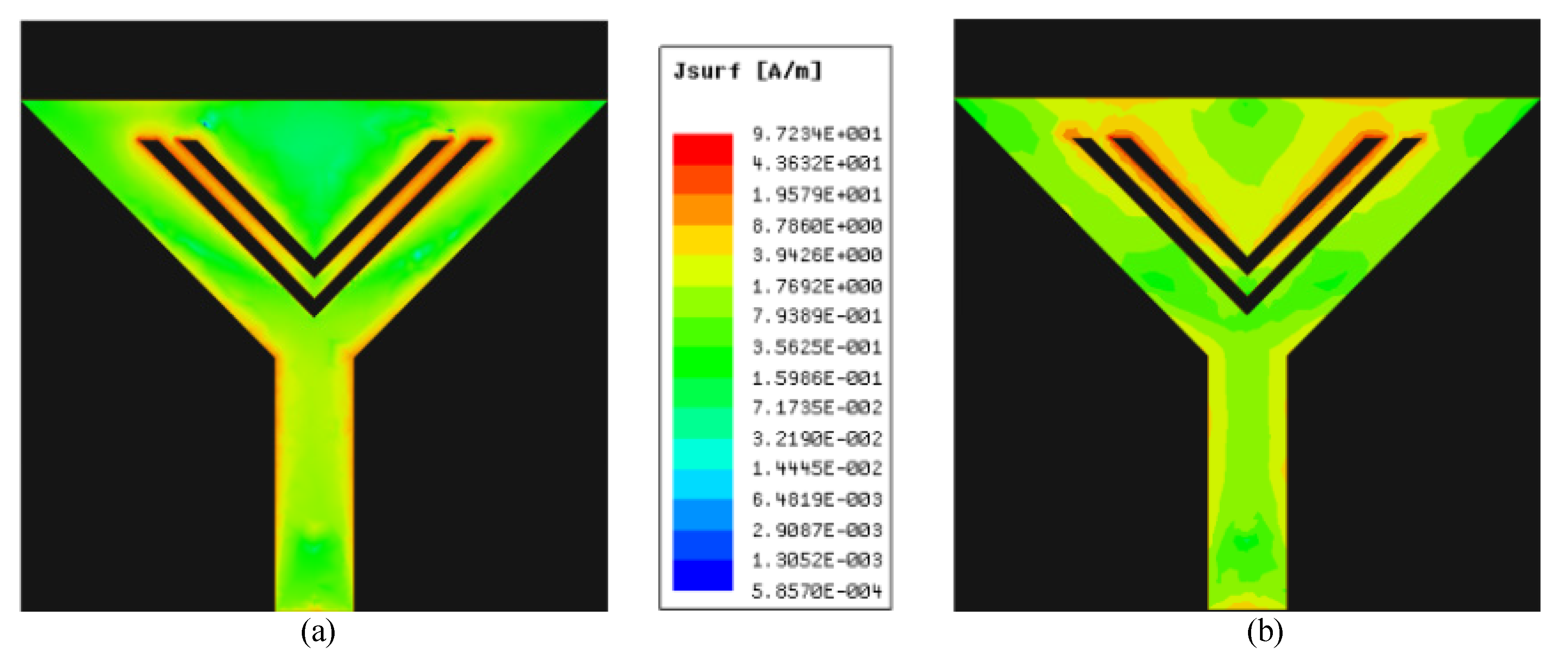
2.5. Numerical Analysis

Figure 5 depicts the equivalent circuit of the UWB antenna along with the UWB antenna with a single and dual-notch band. The equivalent model of the UWB antenna was designed using a series-connected combination of RLC components, where each group of RLC components show the independent single resonance. The operational region of each resonance overlaps due to closely spaced thus results in a Wide Band Antenna (WBA) [30,31]. Similarly, the notch bands occurred due to the presence of V-shaped slots were also model using an RLC group, where the LC equivalent notch frequency fno [32].
f n o = 1 2 π 1 L e q C e q  
where Ceq is the total equivalent capacitance and can be obtained by summing up the capacitances generated by individual leg of the V-shaped slot. Leq is the equivalent inductance generated by the etched slot and can be calculated by using the following relation:
L e q = 0.0002 E ( 2.303 log 10 ( 4 E D ) θ ) μ H
where E was assumed to be the finite length of a wire of rectangular cross-section equals to the notch area, D is the length approximately equals to the cross-section of the slot, and θ is the angle between the legs of the V-shaped slot.
As the current distribution is perturbed due to slots on the radiating patch, the path of the current is elongated. The length of the current path exhibits the series inductance, whereas the etched gaps of the slots accumulate the charge, hence determines series capacitance. Collectively, this behavior can be represented by the equivalent lumped element circuit with LC configuration. The equivalent lumped element parallel RLC circuit for the proposed antenna is illustrated in Figure 5. LS1, CSi, and RSi represent the inductance, capacitance, and radiation resistance for ith radiating mode at each resonant frequency band, respectively. The lumped effect of the slots causing the resonant frequency is represented as a series combination of all lumped elements with an inductive patch antenna and ground plane as a capacitive load. Both inductive and capacitive effects as well as feeding effects are considered for higher-order modes generation and significantly contribute to the input impedance of the antenna.

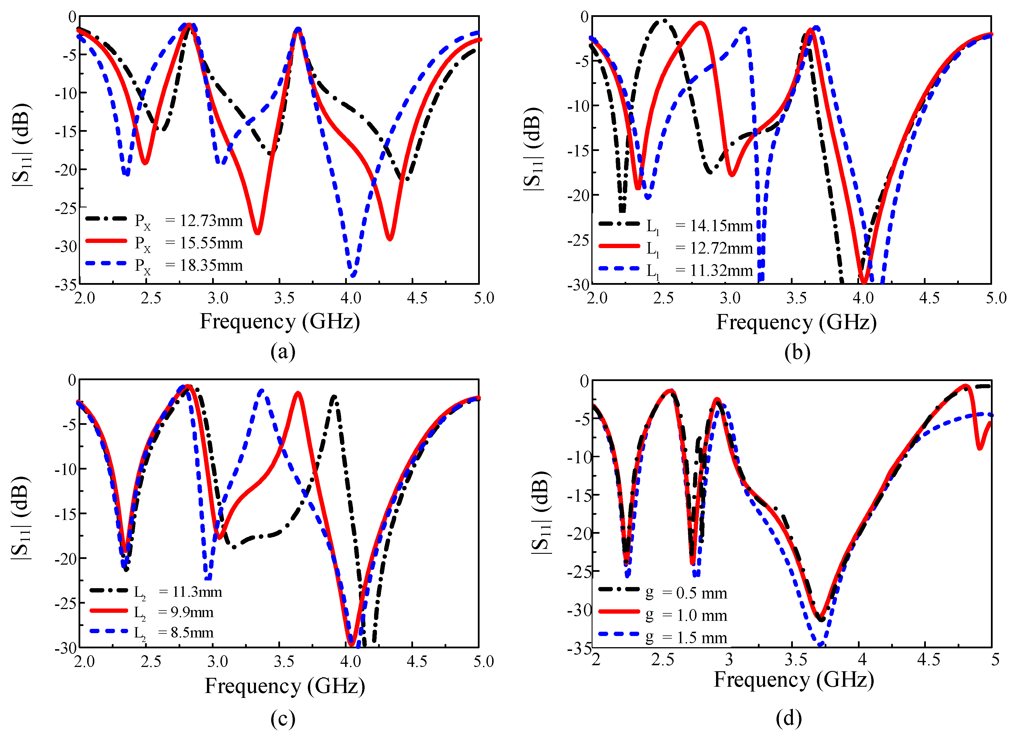
2.6. Parametric Analysis

Parametric analysis of the key parameters of the antenna is performed to investigate their effects on the performance of the antenna, as depicted in Figure 6. As shown in Figure 6a, when the length of the truncated corner was changed from 15.55 mm to 12.73 mm, all the resonances were shifted toward the higher side. An increment in bandwidth was observed for the third while the bandwidth of the first resonance decreases considerably, as depicted in Figure 6a. On the other hand, when the value of PX was increased from 15.55 mm to 18.35 mm, all resonances shift toward the lower side along with a decrement in the bandwidth of the third resonance. The increase and decrease in the bandwidth are due to the number of current passes from feedline to radiator while the shift in resonance toward lower and higher frequency is due to change in the effective length of the radiator, as discussed earlier in Section 2.2. It is worthy to note that the notched frequencies remain unchanged for both higher and lower variations, as depicted in Figure 6a.
Figure 6b illustrates the effects of variation in the dimension of L1. It could be observed that when the value of L1 has increased from 12.72 mm to 14.15 mm the first notch band shifts from 2.8 GHz to 2.55 GHz, also the bandwidth of the first resonance decreases while the bandwidth of the second resonance increases as depicted in Figure 6b. On the other hand, when the value of L1 was decreased to 11.32 mm, the notch band shifted to 3.1 GHz along with increased bandwidth at first resonance and decreased bandwidth at the second resonance. A similar phenomenon was also observed for the second notch band by varying the dimension of L2, as depicted in Figure 6c. It is worthy to note that the second notch band and third resonance remain conserved for all variation in L1 while the first notch and first resonance remain conserved for all variation in L2. Moreover, from Figure 6d, it could also be observed that the gap between the slots (g) also has less impact of the performance of the antenna. Thus, the proposed antenna becomes a promising candidate for the application where independently controllable notch band antennas are required.

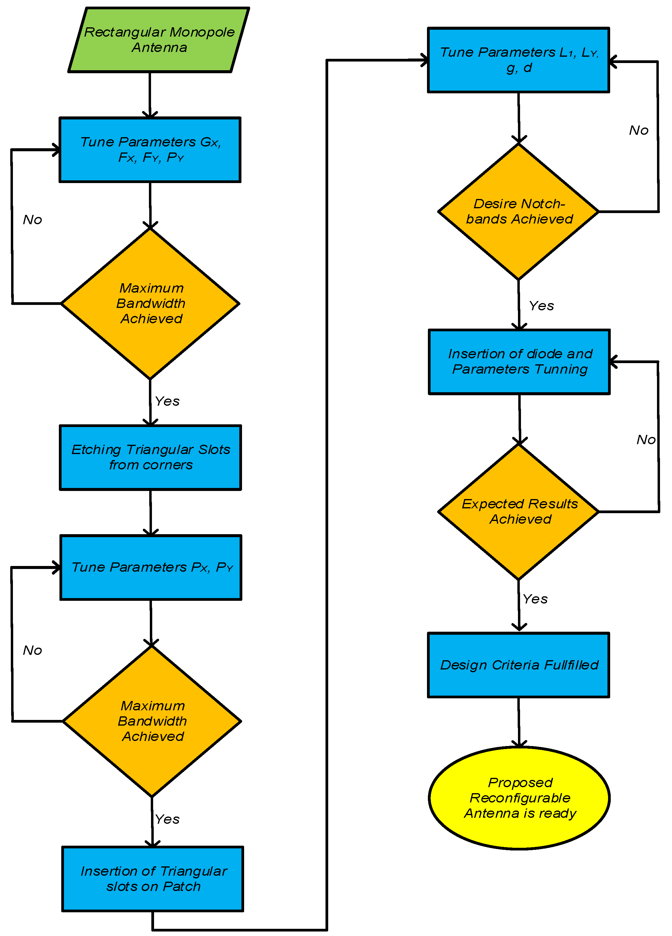
2.7. Design Methodology

Figure 7 depicts the flow chart of the design methodology of the proposed antenna. Initially, a quarter-wave rectangular monopole antenna was designed. Various parameters of monopole, including length and width of the radiator, feedline, and truncated ground plane, were optimized to get maximum bandwidth. Afterwards, lower corners of the monopole radiator were truncated by using an equilateral triangle such that the hypotenuse of the triangle is PX.
The hypotenuse of the triangular slot and width of the radiator was further optimized to get the ultra-wide bandwidth. The resultant antenna shows an impedance bandwidth of 62.8%. In the next step, two triangular slots were etched from the radiator to achieve two notch bands from an already designed ultra-wideband antenna. The length and width slot along with separation between them were well-tuned to achieve the desire notch bands. The resultant antenna exhibits a tri-band operational mode along with two notch bands where the value of S11 is greater than −2 dB. Finally, two RF-PIN diodes were inserted at the center of the slots, such that when the diode is in ON-state the slot becomes inactive while in OFF-state the slot becomes active and a notched band is achieved. Biasing circuits were designed at the backside of the antenna to minimize the effects of basing components and wires. Final tuning of various parameters was performed due to the addition of diodes, capacitors, and inductors to achieve the desired frequency reconfigurable antenna having dual-band, tri-band, and wideband operational mode.

3. Results and Discussion

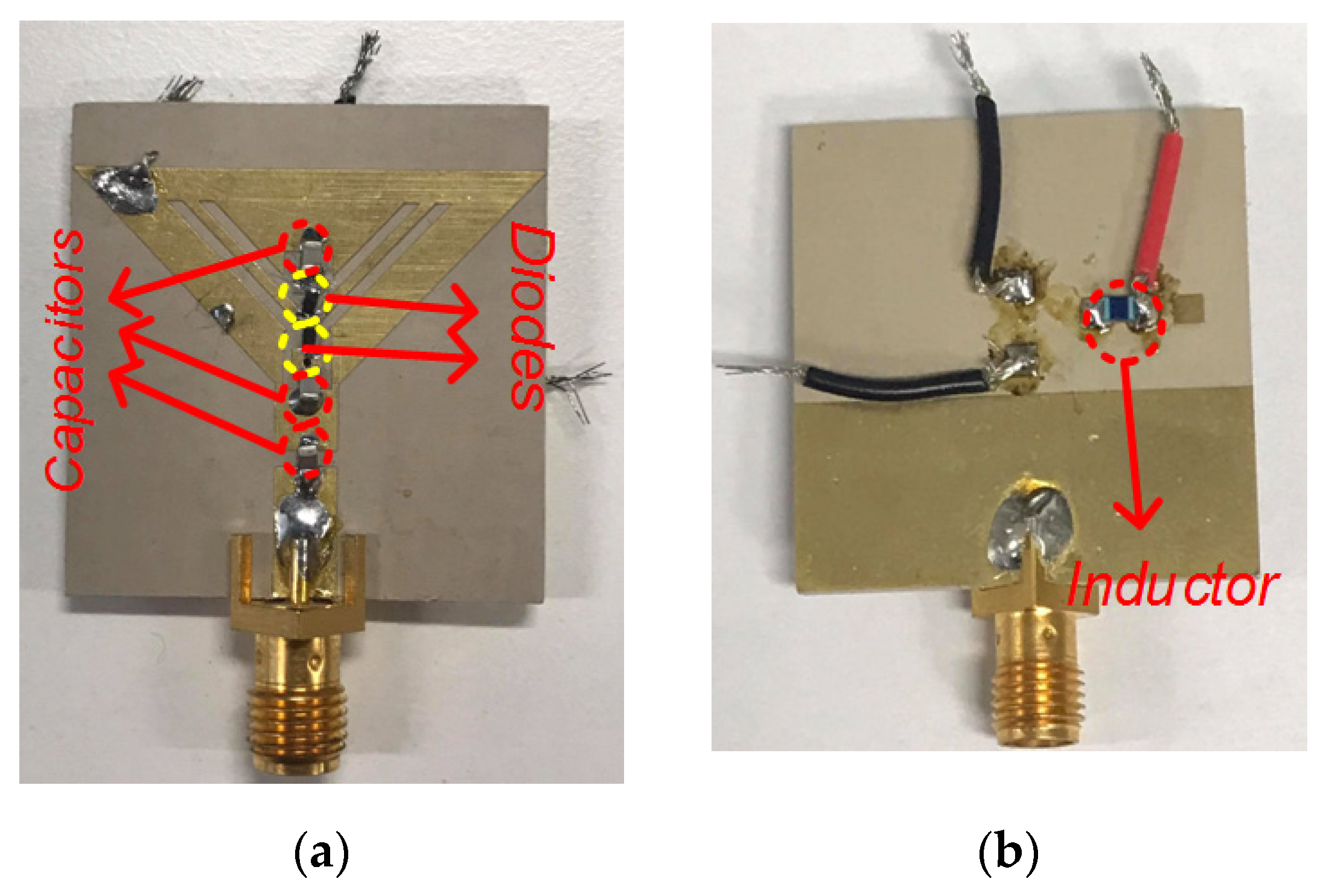
3.1. Measurement Setup
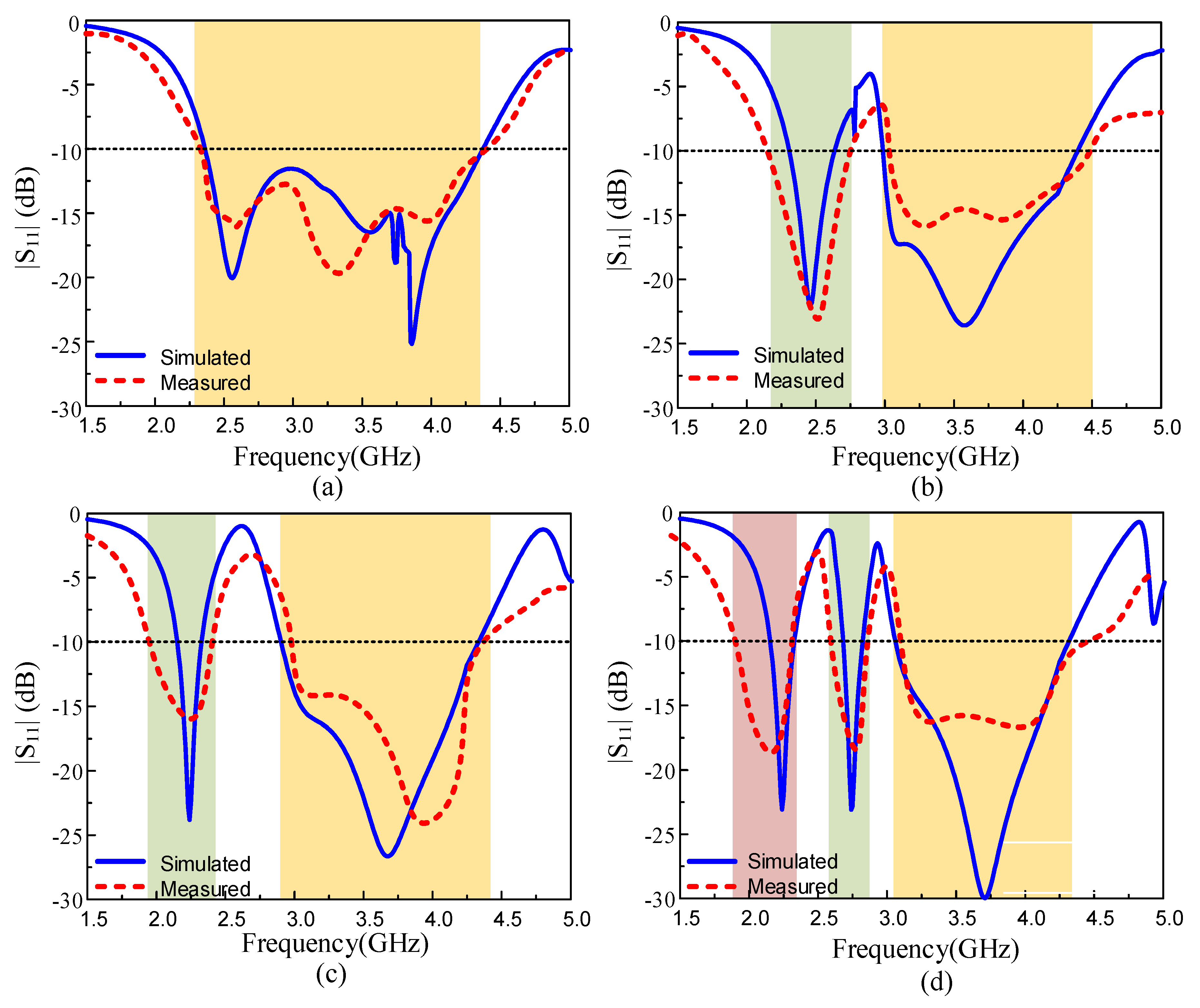
To measure the S-parameters of the proposed antenna, the Anritsu S820E Antenna Analyzer is used. Figure 8 shows the fabricated antenna prototype. The far-field characteristics of the antenna are measured through a commercial far-field measurement system in a shielded RF anechoic chamber. The horn antenna (SGH-series) having a standard gain of 24 dBi is utilized as a transmitter, while the proposed antenna was measured as a receiving antenna. Power amplifiers were used to provide stable power reception. The antenna is rotated in 360° to measure the far-field results.

3.2. S-Parameter

Figure 9 shows the simulated and measured S11. It can be observed that the antenna either operates in wideband mode, two dual-band modes, and tri-band mode, as depicted in Figure 9a–d. The biasing voltage of the PIN diode is 3V. When both diodes D1 and D2 were in ON state, which refers to case-11, the antenna act as a wideband antenna having S11 < −10 dB impedance predicted bandwidth of 2.29–4.47 GHz whereas, the measured bandwidth was observed to be 2.25–4.53 GHz, as depicted in Figure 9a. When either the diode D1 or D2 was kept in On-state while keeping the other diode in Off-state the antenna exhibits dual-band mode, as depicted in Figure 9b,c. The predicted bandwidth of the proposed antenna for case—01 was observed to be 2.3–2.65 GHz and 3–4.5 GHz, while for case-10 it was observed to be 2.1–2.4 GHz and 2.92–4.37 GHz, respectively.
On the other hand, the measured S11 < −10 dB bandwidth for case-01 was observed to be 2.1–2.78 GHz and 3.09–4.57 GHz, respectively, as depicted in Figure 9b, while for case-10 it was observed to be 1.86–2.5 GHz and 3.03–4.47 GHz, as depicted in Figure 9c. At last, when both diodes were kept in Off-state, referring to case-00, the antenna exhibits triband operational mode having predicted passbands of 2.17–2.35 GHz, 2.64–2.85 GHz, and 3.09–4.34 GHz. The measured impedance bandwidths for case-00 were reported to be 1.93–2.4 GHz, 2.62–2.97 GHz, and 3.2–4.65 GHz, as depicted in Figure 9d. In general, a strong agreement was observed between simulated and measured results, while the small discrepancy between the results was owing to fabrication and measurement circuitry.

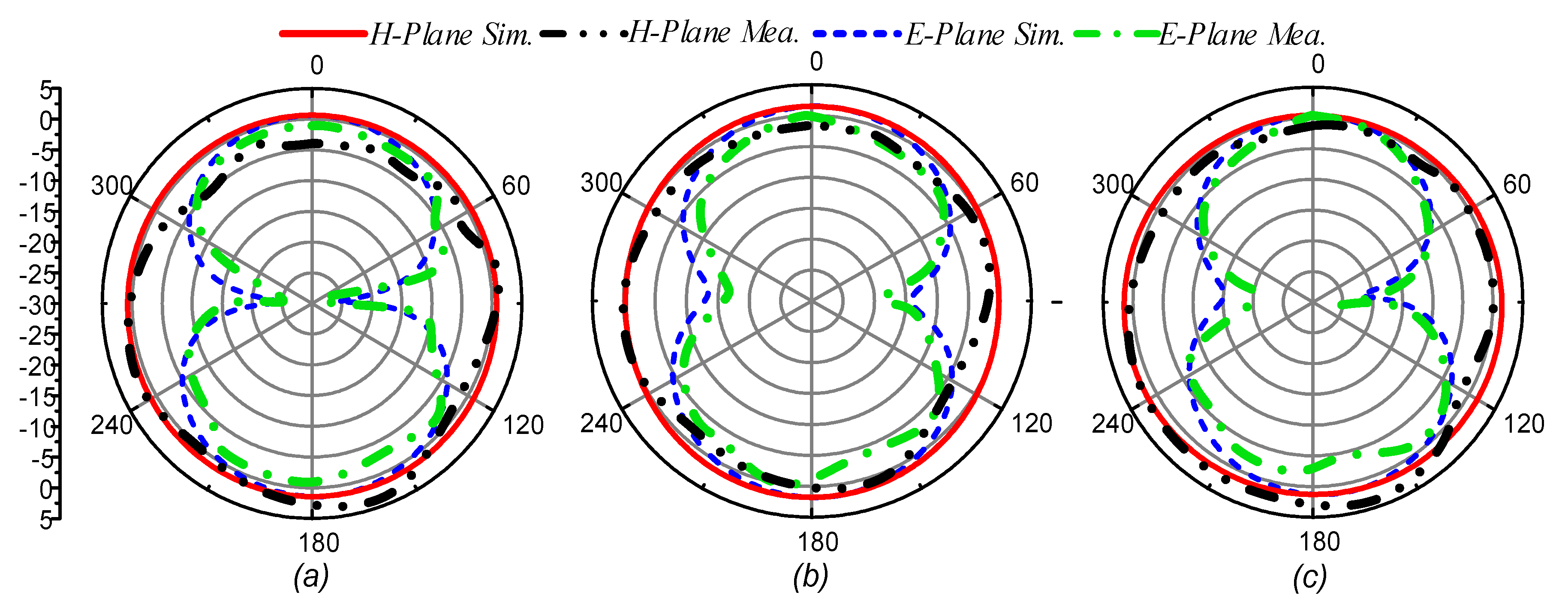
3.3. Radiation Patterns

Figure 10 illustrates the simulated and measured radiation patterns of the proposed antenna at resonating frequencies for various switching states. For all resonating frequencies, the antenna exhibits an omnidirectional radiation pattern in principle H-plane (θ = 90°). On the other hand, for all resonating frequencies, the antenna exhibits a monopole like bi-directional radiation pattern in principle E-Plane (θ = 0°). Moreover, it is observed for all switching states that the proposed antenna shows good agreement between simulated and measured results.

3.4. Gain and Radiation Efficiency

Figure 11 shows the predicted and measured gain of the proposed reconfigurable antenna. It can be seen from Figure 11a, when both diodes are in ON-state the antenna exhibits a gain of <2.5 dBi in the operational band along with radiation efficiency of <90%. However, the antenna in multiband mode shows the gain of <2.4 dBi in passband regions along with radiation efficiency of <89% (Figure 11b–d), while for the band stop region the gain and radiation efficiency of the proposed antenna decreases up to −8 dBi and 22%, respectively. A strong agreement between simulated and measured results state the performance stability of the antenna. Table 2 shows the comparison between measured and simulated results for different states of PIN diodes.

3.5. Comparison with State-of-the-Art Works

Table 3 presents the comparison of the proposed antenna with state-of-the-art works for similar applications. It could be observed clearly that the proposed antenna overperforms the existing antennas by providing the best combination of compact size, multi-mode operation, wide operational region, relatively high gain, and simple geometrical structure.

4. Conclusions

A compact frequency reconfigurable antenna is proposed in this paper. Initially, to cover 5G sub—6 GHz band, a wideband triangle-shaped monopole antenna was designed, which was originally inspired from a rectangular monopole antenna. Afterwards, two V-shaped slots were utilized to achieve two notch bands, their length could be adjusted independently to achieve the desire notch bands. Finally, two RF-PIN diodes were inserted at the middle of the slots such that when diodes are in Off-state they active the slot and thus result in notching the band. The overall size of the antenna is 0.19λo × 0.19λo × 0.0081λo, where λo correspond to the free space wavelength at the lowest resonating frequency. The proposed antenna can operate in wideband mode, two different dual-band modes, or tri-band, depending upon the state of the diodes. Strong agreement between predicted and measured results, along with reasonable gain in passbands and very low gain in the band-stop region, makes the proposed antenna a suitable candidate for 2.1 GHz 4G-LTE band, 2.45 GHz ISM band, 5G-sub-6 GHz band, and S-band applications.

Author Contributions

Conceptualization: A.G., W.A.A., and M.A.; methodology, A.G., N.H. and S.I.N.; software, A.G., W.A.A., N.H., and X.J.L.; validation, A.G., S.I.N., and M.A.; investigation, A.G., W.A.A., S.I.N., and M.A.; resources, M.A., F.F., and E.L.; writing—original draft preparation, A.G., W.A.A., and N.H.; writing—review and editing, X.J.L., B.-C.S., S.I.N., M.A., F.F., and E.L.; supervision, X.J.L., and B.-C.S. All authors have read and agreed to the published version of the manuscript.

Funding

This research received no external funding.

Institutional Review Board Statement

Not applicable.

Informed Consent Statement

Not applicable.

Data Availability Statement

Data is contained within the article.

Acknowledgments

This work is partially supported by RTI2018-095499-B-C31, Funded by Ministerio de Ciencia, Innovación y Universidades, Gobierno de España (MCIU/AEI/FEDER,UE).

Conflicts of Interest

The authors declare no conflict of interest.

References

  1. Nikolaou, S.; Bairavasubramanian, R.; Lugo, C.; Carrasquillo, I.; Thompson, D.C.; Ponchak, G.E.; Papapolymerou, J.; Tentzeris, M.M. Pattern and frequency reconfigurable annular slot antenna using PIN diodes. IEEE Trans. Antennas Propag. 2006, 54, 439–448. [Google Scholar] [CrossRef]
  2. Ojaroudi, N.P.; Basherlou, H.J.; Al-Yasir, Y.I.A.; Abd-Alhameed, R.A.; Abdulkhaleq, A.M.; Noras, J.M. Recent Developments of Reconfigurable Antennas for Current and Future Wireless Communication Systems. Electronics 2019, 8, 128. [Google Scholar] [CrossRef] [Green Version]
  3. Ghaffar, A.; Li, X.J.; Seet, B.-C. Dual frequency band and polarization reconfigurable antenna for mobile devices. In Proceedings of the IEEE 17th International Conference on Communication Technology (ICCT), Chengdu, China, 23–27 October 2017. [Google Scholar]
  4. Boufrioua, A. Frequency Reconfigurable Antenna Designs Using PIN Diode for Wireless Communication Applications. Wirel. Pers. Commun. 2019, 110, 1879–1885. [Google Scholar] [CrossRef]
  5. Affandi, A.; Azim, R.; Alam, M.; Islam, M.T. A Low-Profile Wideband Antenna for WWAN/LTE Applications. Electronics 2020, 9, 393. [Google Scholar] [CrossRef] [Green Version]
  6. Zaidi, A.; Awan, W.A.; Hussain, N.; Baghdad, A. A Wide and Tri-band Flexible Antennas with Independently Controllable Notch Bands for Sub-6-GHz Communication System. Radioengineering 2020, 29, 44–51. [Google Scholar] [CrossRef]
  7. Jin, G.; Deng, C.; Yang, J.; Xu, Y.; Liao, S. A New Differentially-Fed Frequency Reconfigurable Antenna for WLAN and Sub-6GHz 5G Applications. IEEE Access 2019, 7, 56539–56546. [Google Scholar] [CrossRef]
  8. Cai, Y.-M.; Li, K.; Yin, Y.; Gao, S.; Hu, W.; Zhao, L. A Low-Profile Frequency Reconfigurable Grid-Slotted Patch Antenna. IEEE Access 2018, 6, 36305–36312. [Google Scholar] [CrossRef]
  9. Wang, J.; Yang, L. A compact four bands microstrip patch antenna with coplanar waveguide feed. In Proceedings of the 3rd Asia-Pacific Conference on Antennas and Propagation, Harbin, China, 26–29 July 2014; pp. 33–36. [Google Scholar]
  10. Feng, G.; Guo, C.; Ding, J. Frequency-Reconfigurable Slot Antenna Using Metasurface. In Proceedings of the International Conference on Microwave and Millimeter Wave Technology (ICMMT), Chengdu, China, 7–11 May 2018. [Google Scholar]
  11. Zhao, X.; Riaz, S. A Dual-Band Frequency Reconfigurable MIMO Patch-Slot Antenna Based on Reconfigurable Microstrip Feedline. IEEE Access 2018, 6, 41450–41457. [Google Scholar] [CrossRef]
  12. Soltanpour, M.; Fakharian, M. Compact filtering slot antenna with frequency agility for Wi-Fi/LTE mobile applications. Electron. Lett. 2016, 52, 491–492. [Google Scholar] [CrossRef]
  13. Han, L.; Wang, C.; Chen, X.; Zhang, W. Compact Frequency-Reconfigurable Slot Antenna for Wireless Applications. IEEE Antennas Wirel. Propag. Lett. 2016, 15, 1795–1798. [Google Scholar] [CrossRef]
  14. Ali, T.; Biradar, R.C. A compact hexagonal slot dual band frequency reconfigurable antenna for WLAN applications. Microw. Opt. Technol. Lett. 2017, 59, 958–964. [Google Scholar] [CrossRef]
  15. Abdulraheem, Y.I.; Oguntala, G.A.; Abdullah, A.S.; Mohammed, H.J.; Ali, R.A.; Abd-Alhameed, R.A.; Noras, J.M. Design of frequency reconfigurable multiband compact antenna using two PIN diodes for WLAN/WiMAX applications. IET Microw. Antennas Propag. 2017, 11, 1098–1105. [Google Scholar] [CrossRef] [Green Version]
  16. Ali, T.; Khaleeq, M.M.; Biradar, R.C. A multiband reconfigurable slot antenna for wireless applications. AEU Int. J. Electron. Commun. 2018, 84, 273–280. [Google Scholar] [CrossRef]
  17. Saraswat, K.; Harish, A.R. Flexible dual-band dual-polarised CPW-fed monopole antenna with discrete-frequency reconfigurability. IET Microw. Antennas Propag. 2019, 13, 2053–2060. [Google Scholar] [CrossRef]
  18. Abbas, A.; Hussain, N.; Jeong, M.-J.; Park, J.; Shin, K.S.; Kim, T.; Kim, N. A Rectangular Notch-Band UWB Antenna with Controllable Notched Bandwidth and Centre Frequency. Sensors 2020, 20, 777. [Google Scholar] [CrossRef] [Green Version]
  19. Ghaffar, A.; Li, X.J.; Seet, B.-C.; Awan, W.A.; Hussain, N. Compact Multiband Frequency Reconfigurable Antenna for 5G Communications. In Proceedings of the 29th International Telecommunication Networks and Applications Conference (ITNAC), Auckland, New Zealand, 27–29 November 2019; pp. 1–3. [Google Scholar]
  20. Awan, W.A.; Hussain, N.; Le, T.T. Ultra-thin flexible fractal antenna for 2.45 GHz application with wideband harmonic rejection. AEU Int. J. Electron. Commun. 2019, 110, 152851. [Google Scholar] [CrossRef]
  21. ROGERS Corporation. Available online: www.rogerscorp.com (accessed on 10 July 2020).
  22. Balanis, C.A. Antenna Theory: Analysis and Design; John Wiley & Sons: Hoboken, NJ, USA, 2016. [Google Scholar]
  23. Yang, X.; Luyen, H.; Xu, S.; Behdad, N. Design Method for Low-Profile, Harmonic-Suppressed Filter-Antennas Using Miniaturized-Element Frequency Selective Surfaces. IEEE Antennas Wirel. Propag. Lett. 2019, 18, 427–431. [Google Scholar] [CrossRef]
  24. Hussain, N.; Awan, W.A.; Naqvi, S.I.; Ghaffar, A.; Zaidi, A.; Iftikhar, A.; Li, X.J. A Compact Flexible Frequency Reconfigurable Antenna for Heterogeneous Applications. IEEE Access 2020, 8, 173298–173307. [Google Scholar] [CrossRef]
  25. Rahman, S.U.; Cao, Q.; Wang, Y.; Ullah, H. Design of wideband antenna with band notch characteristics based on single notching element. Int. J. RF Microw. Comput. Eng. 2018, 29, e21541. [Google Scholar] [CrossRef]
  26. Luo, S.; Chen, Y.; Wang, D.; Liao, Y.; Li, Y. A monopole UWB antenna with sextuple band-notched based on SRRs and U-shaped parasitic strips. AEU Int. J. Electron. Commun. 2020, 120, 153206. [Google Scholar] [CrossRef]
  27. Khan, M.S.; Naqvi, S.A.; Iftikhar, A.; Asif, S.M.; Fida, A.; Shubair, R.M. A WLAN band-notched compact four element UWB MIMO antenna. Int. J. RF Microw. Comput. Eng. 2020, 30, e22282. [Google Scholar] [CrossRef]
  28. Park, J.; Jeong, M.; Hussain, N.; Rhee, S.; Park, S.; Kim, N. A low-profile high-gain filtering antenna for fifth generation systems based on nonuniform metasurface. Microw. Opt. Technol. Lett. 2019, 61, 2513–2519. [Google Scholar] [CrossRef]
  29. Hussain, N.; Jeong, M.; Park, J.; Rhee, S.; Kim, P.; Kim, N. A compact size 2.9–23.5 GHz microstrip patch antenna with WLAN band-rejection. Microw. Opt. Technol. Lett. 2019, 61, 1307–1313. [Google Scholar] [CrossRef]
  30. Awan, W.A.; Zaidi, A.; Hussain, N.; Iqbal, A.; Baghdad, A. Stub loaded, low profile UWB antenna with independently controllable notch-bands. Microw. Opt. Technol. Lett. 2019, 61, 2447–2454. [Google Scholar] [CrossRef]
  31. Iqbal, A.; Smida, A.; Mallat, N.K.; Islam, M.T.; Kim, S. A Compact UWB Antenna with Independently Controllable Notch Bands. Sensors 2019, 19, 1411. [Google Scholar] [CrossRef] [Green Version]
  32. Ghimire, J.; Choi, D.-Y. Design of a Compact Ultrawideband U-Shaped Slot Etched on a Circular Patch Antenna with Notch Band Characteristics for Ultrawideband Applications. Int. J. Antennas Propag. 2019, 2019, 1–10. [Google Scholar] [CrossRef] [Green Version]
Figure 1. Geometrical configuration of proposed antenna: (a) top-view (b) bottom-view (c) side-view.
Applsci 11 01635 g001
Figure 2. S11 for rectangular shape monopole with and without truncated corners.
Applsci 11 01635 g002
Figure 3. S11 for wideband antenna and wideband antenna with single and dual-notch bands.
Applsci 11 01635 g003
Figure 4. Current distribution of proposed antenna at notch-band of: (a) 2.82 GHz (b) 3.64 GHz.
Applsci 11 01635 g004
Figure 5. RLC equivalent model of wide band antenna with and without notch-bands.
Applsci 11 01635 g005
Figure 6. Parametric analysis of the various parameters of the antenna: (a) PX (b) L1 (c) L2 (d) g.
Applsci 11 01635 g006
Figure 7. Flow chart of the design methodology of the proposed antenna.
Applsci 11 01635 g007
Figure 8. Fabricated prototype of the proposed antenna: (a) top-view (b) bottom-view.
Applsci 11 01635 g008
Figure 9. Simulated and measured results of S11: (a) case-11 (b) case-01 (c) case-10 (d) case-00.
Applsci 11 01635 g009
Figure 10. Simulated and measured radiation patterns for case-00: (a) 2.24 GHz (b) 2.74 GHz (c) 3.71 GHz.
Applsci 11 01635 g010
Figure 11. Simulated and measured gain along with radiation efficiency: (a) case-11 (b) case-01 (c) case-10 (d) case-00.
Applsci 11 01635 g011
Table 1. Dimension of the various parameter length of the proposed antenna.
ParameterValueParameterValueParameterValue
AX30 mmAY30 mmH1.9 mm
GX12 mmFX30 mmFY1.9 mm
PX15.55 mmPY30 mmg1 mm
d1 mmL112.72 mmL29.9 mm
C1100 pFI68 nHCDC100 pF
Table 2. Comparison among simulated and measured values for various switching states.
Switching
State
Diode
State
Simulated Bandwidth
(GHz)
Measured Bandwidth
(GHz)
Simulated
Peak Gain (dBi)
Measured
Peak Gain (dBi)
Case-11D1-On and D2-On2.29–4.472.25–4.533.863.8
Case-01D1-On and D2-Off2.3–2.652.1–2.782.442.39
3–4.53.09–4.573.913.82
Case-10D1-Off and D2-On2.1–2.41.86–2.52.211.89
2.92–4.373.03–4.473.893.82
Case-00D1-Off and D2-Off2.17–2.351.93–2.42.262.17
2.64–2.852.62–2.932.011.96
3.19–4.343.19–4.653.93.79
Table 3. Comparison of the proposed antenna with state-of-the-art works for similar applications.
Ref.Dimension (mm2)Operational ModeReconfigurable TechniqueFrequency
Range
(GHz)
Peak
Gain
(dBi)
[5]65 × 10WidebandN. A1.6–2.22.45
[6]25 × 30Tri-bandN. A2.35–5.53.75
[8]100 × 100Single bandPIN-diode (2)2.2–3.86.5
[9]70 × 70Single bandVaractor (1)2.6–3.85.92
[10]50 × 50Single bandMechanical2–4.55.6
[11]27 × 27Single bandVaractor (1)1.4–2.2.48
[12]14 × 36Single bandPIN-diode (2)2–2.6N. R
[13]25 × 27Single and Dual BandPIN-diode (2)2–62.8
[14]20 × 16Single and Dual BandPIN-diode (2)2–63.13
[15]50 × 45Dual and Tri BandPIN-diode (2)2.5–55.8
[16]30 × 28Dual and Quad bandPIN-diode (1)1.5–113.1
[17]50 × 33Wide and Dual BandPIN-diode (2)2–3.753.2
This Work30 × 30Wide, Dual and Tri bandPIN-diode (2)1.8–4.53.72
Publisher’s Note: MDPI stays neutral with regard to jurisdictional claims in published maps and institutional affiliations.

