Article

A High-Frequency-Compatible Miniaturized Bandpass Filter with Air-Bridge Structures Using GaAs-Based Integrated Passive Device Technology

1
Radio Frequency Integrated Circuit (RFIC) Center, Kwangwoon University (01897), 20 Gwangwun-ro, Nowon-ku, Seoul 139-701, Korea
2
Harbin Institute of Technology, School of Information and Engineering, Harbin 15001, China
*
Author to whom correspondence should be addressed.
Micromachines 2018, 9(9), 463; https://doi.org/10.3390/mi9090463
Submission received: 31 July 2018 / Revised: 8 September 2018 / Accepted: 9 September 2018 / Published: 13 September 2018
(This article belongs to the Special Issue Selected Papers from IEEE ICASI 2018)

Abstract

:
This paper reports on the use of gallium arsenide-based integrated passive device technology for the implementation of a miniaturized bandpass filter that incorporates an intertwined circle-shaped spiral inductor and an integrated center-located capacitor. Air-bridge structures were introduced to the outer inductor and inner capacitor for the purpose of space-saving, thereby yielding a filter with an overall chip area of 1178 μm × 970 μm. Thus, not only is the chip area minimized, but the magnitude of return loss is also improved as a result of selective variation of bridge capacitance. The proposed device possesses a single passband with a central frequency of 1.71 GHz (return loss: 32.1 dB), and a wide fractional bandwidth (FBW) of 66.63% (insertion loss: 0.50 dB). One transmission zero with an amplitude of 43.42 dB was obtained on the right side of the passband at 4.48 GHz. Owing to its miniaturized chip size, wide FBW, good out-band suppression, and ability to yield high-quality signals, the fabricated bandpass filter can be implemented in various L-band applications such as mobile services, satellite navigation, telecommunications, and aircraft surveillance.

1. Introduction

With the rapid development of modern wireless and telecommunication systems, microwave filters have come to play an important role in various radio frequency (RF)/microwave applications because they allow frequency selection. Among the various types of microwave filters, bandpass filters (BPFs) have been extensively studied as a key building block in the design of RF/microwave integrated circuits and systems. However, emerging applications continue to challenge BPF efficacy with increasingly rigorous demands for lower cost, smaller size, higher performance, etc. [1,2,3].
To satisfy the increasingly stringent requirements of RF and microwave systems, a wide range of materials and techniques that can be used to modify existing lumped passive components have been incorporated into recently developed fabrication processes [4]. Recent advances in novel fabrication techniques, including the implementation of low-temperature co-fired ceramics (LTCC), high-temperature superconductor (HTS), micro-electromechanical system (MEMS), monolithic microwave integrated circuit (MMIC), and micro-fabrication techniques, have accelerated the rapid development of filters for various RF/microwave applications [5]. With LTCC technology, a variety of passive components such as strip lines, filters, antennas, and resonators, which are manufactured by using inexpensive yet highly conductive metals with low electrical resistance and low conductor loss at high frequencies, can be employed. However, this technology has two major disadvantages: (1) Post-firing ceramic shrinkage limits the size of the board to be processed, and (2) modules that require heat dissipation must be equipped with a heat sink that is applied after heating [6]. High-temperature superconductors are attractive because of their very low surface resistance in comparison to even the most conductive normal metals. Furthermore, their low loss properties allow the microwave passive components to be fabricated with a far more compact geometry than that of conventional materials. Despite its well-known advantages, the high cost and increased system complexity during low-temperature operation prevent HTS technology from being widely applied [7]. Micro-electromechanical system processing enables the batch fabrication of miniature structures that range in size from a few micrometers to a few millimeters; this technique facilitates cost, size, and weight reductions. Furthermore, the ability to seamlessly integrate mechanical components into electronics at the same wafer level is one of the most prominent properties of MEMS technology. However, MEMS components have a considerably short life cycle in addition to undefined power handling capability and an unstable ultimate dynamic range [8]. Alternatively, gallium arsenide and other advanced III–V materials allow MMICs to be applied in the millimeter wavelength region with increased functional capability, improved system reliability, and reduced weight, volume, and cost [9]. The major drawback of this technology is that the circuits can yield performance results for certain parameters that are worse than those observed from the same devices made with separate components [10].
Recently, some groups are researching the implementation of BPFs with emerging technologies such as complementary metal-oxide-semiconductor (CMOS) and stimulated Brillouin scattering (SBS). With regard to low-cost mass production, high integration capability, and lower power consumption, CMOS has proven to be a promising fabrication technique. However, this technology causes serious issues in the realization of high-quality passive components due to losses, especially at high frequencies [11,12,13]. Stimulated Brillouin scattering-based microwave photonics filtering has attracted significant interest over classical microwave techniques for its low propagation loss, ultra-broad transmission bandwidth, light-weight, and small-footprint. The bandwidth of the SBS-based filter can be adjusted by tailoring the pump profile and therefore provides the device with wide bandwidth tunability (MHz–GHz). Apart from the perfection, the SBS-based device is hard to be monolithically integrated with other on-chip photodetectors and electro-optic modulators [14,15,16]. In general, lumped elements have a lower Q value (for CMOS, Q factor is less than 15) [17,18]; to some extent, this problem can be mitigated by implementing integrated passive device (IPD) technology (Q factor >30), as is described in our previous reports [19,20,21,22]. Integrated passive device technology employs a newly developed fabrication technique that achieves the desired trade-off for package integration systems and affords complete module solutions; thus, overall improved system performance can be achieved through integration with other functionalities. This technique facilitates the design of a simplified and compact passive module with excellent parametric control capability and higher performance as compared to standard discrete systems owing to the reduced parasitic effect.
In this paper, we describe the design and implementation of a miniaturized bandpass filter with air-bridge structures that is fabricated on a gallium arsenide substrate by using IPD technology and is purposed for RF/microwave applications. An equivalent circuit was constructed for the model in consideration of the second-order parasitic effect that is generated under the condition of high frequency. Additionally, the current density was simulated at four selected frequency points by using a three-dimensional (3D) electromagnetic (EM) current simulator. Then, the influence of the inner radius of the BPF was experimentally investigated from the perspective of the S-parameter and lumped parameters.

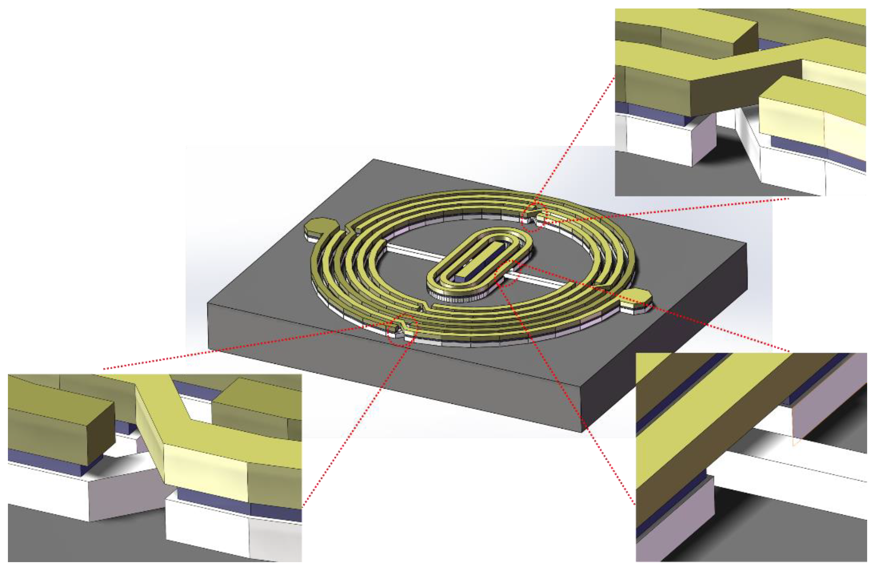
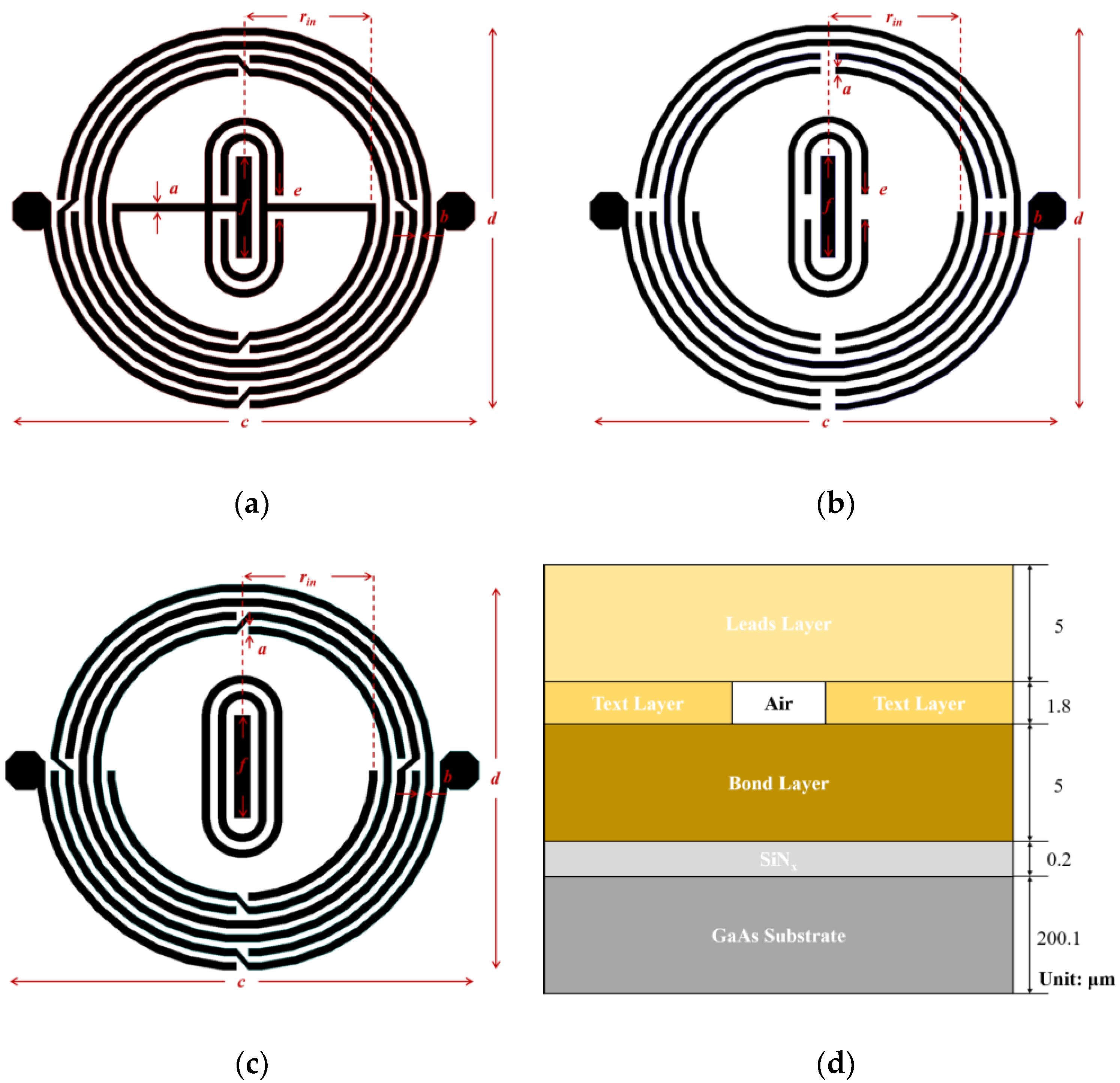
2. Materials and Methods

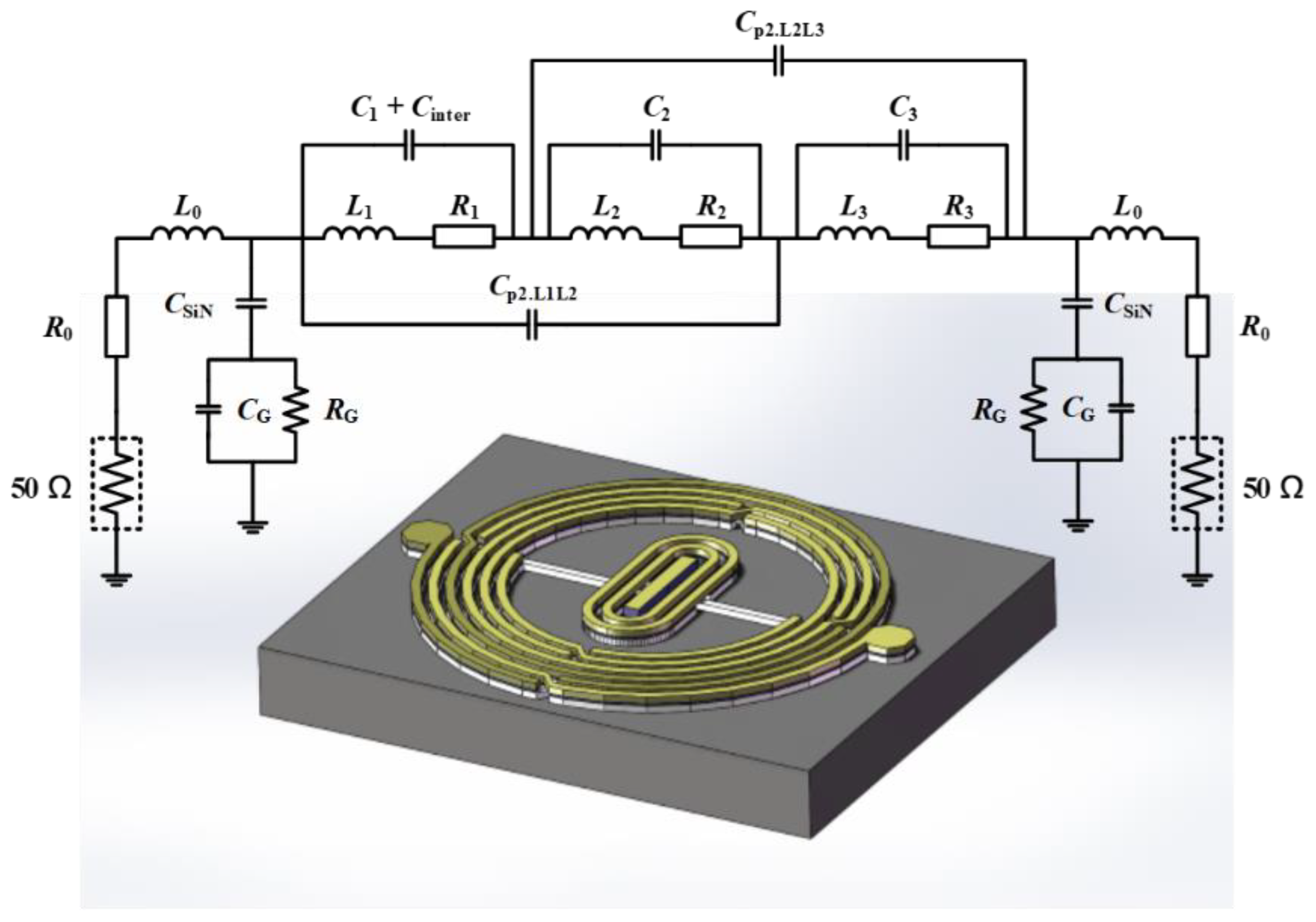
2.1. Equivalent Circuit

As illustrated in Figure 1, a quasi-interdigital capacitor was fabricated between the two divisions of a circle-shaped spiral inductor to build up a compact RF resonator. The proposed BPF was constructed with three copper layers, which, from bottom to top, are the Bond layer, Text layer, and Leads layer, having thicknesses of 5 μm, 1.8 μm, and 5 μm, respectively. Figure 2a–c illustrates the configurations of each of these three layers; their geometric parameters are respectively listed in Table 1, Table 2 and Table 3. A schematic diagram showing the cross-sectional view of the fabricated chip for the IPD is presented in Figure 2d.
The proposed BPF can be simplified as an LC resonant circuit, where an inductor (L) and a capacitor (C) are connected and have a resonant frequency, which is determined by the equation below:
f 0 = 1 2 π L C
where L and C denote the inductance and capacitance, respectively. Moreover, the transmission zero can be derived using:
w 0 = ω mid Ω c × F B W + ( Ω c × F B W ) 2 + 4 2
where ω mid is the midband frequency, Ω c is the passband cut-off frequency of the higher frequency area, and F B W is the fractional bandwidth, which can be calculated using:
F B W = ω 2 ω 1 ω 0
and
ω 0 = ω 1 ω 2
where ω 1 and ω 2 indicate the passband-edge angular frequency, and ω 0 denotes the center frequency.
Figure 3 illustrates the complex equivalent circuit model with three laminated layers; R0 and L0 represent the resistance and inductance, respectively, of the electrodes and terminations. Because of parasitic effects, the capacitance and resistance of the substrate between the planar pattern and ground take the form of CG and RG, respectively [23]. Ri, Li, and Ci (i = 1, 2, 3) are the resistance, inductance, and coupling capacitance between neighboring turns of the Bond layer, Text layer, and Leads layer, respectively. In addition, Cinter is the capacitance of the inner quasi-interdigital capacitor of the bottom Bond layer. Moreover, CSiN is the capacitance of the SiNx layer between the substrate and the pattern.
The proposed BPF has a multilayer structure, which induces various parasitic effects at high frequencies [24]. The second-order coupling capacitance Cp2 represents the parasitic effect between two adjacent layers and was implemented at high frequencies. The coupling capacitance between these layers is related to the number of layers, the overlay area, and the relative dielectric constant of the materials.
The above-listed parameters CG, RG, CSiN, Ri, Li, Ci, and Cinter were calculated as follows:
C G = 1 2 l W C sub
R G = 2 l W G sub
C SiN = 1 2 l W ε SiN t SiN
where C sub and G sub are the capacitance and conductance per unit area of the gallium arsenide substrate, and ε SiN and t SiN are the dielectric constant and thickness of the SiNx layer separating the pattern and substrate, respectively.
Then,
R i = ρ l W δ ( 1 e t / δ )
L i = 0.002 l ( l n 2 l W + t + 0.50049 + W + t 3 l )
C i = 1 L i ( 2 π f 0 ) 2
C inter = 0.10 × ε r l W
where ρ is the resistance coefficient, l is the total circle length, W is the conductor width, δ is the skin depth, t is the thickness of the metal line, f 0 is the resonance frequency, ε r is the dielectric constant, l is the finger length, and W is the finger width [25].

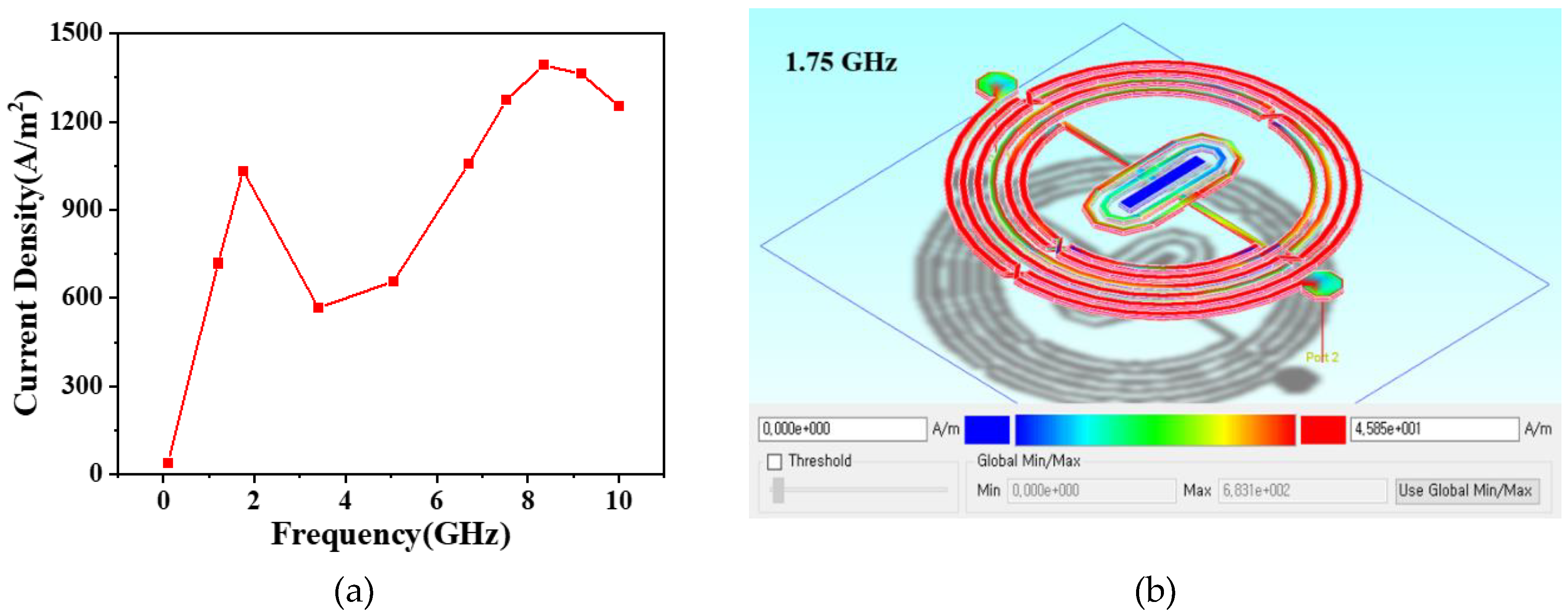
2.2. Current Density

Advanced Design System (ADS) software (Version 2016.01, Keysight Technologies, Inc., Santa Rosa, CA, USA) was employed as a unified interface to simulate momentum in an electromagnetic simulation purpose to evaluate the system design in terms of S-parameter calculation accuracy, surface current, and fields of various planar circuits, including microstrip, stripline, coplanar waveguide, slotline, and other topologies. Interlayer topologies such as air-bridges and vias were incorporated to enable the simulation of multilayer RF/microwave-based printed circuit boards (PCBs), integrated circuits, and multichip modules. Additionally, the simulation was performed in 3D in order to yield a more comprehensive representation of the current flow through slots and conductors through varying degrees of shading, arrows, and contours. The simulated frequency points were selected adaptively for the computation performed through a wide frequency domain that will require a large amount of CPU hardware resources and disk space. Thus, although the frequency range for the electromagnetic (EM) simulation setup was set as 0.1 GHz to 10 GHz, the following 10 frequency points were selected and implemented in the simulation: 0.1 GHz, 1.2 GHz, 1.75 GHz, 3.4 GHz, 5.05 GHz, 6.7 GHz, 7.525 GHz, 8.35 GHz, 9.175 GHz, and 10 GHz. Figure 4a shows the variation of current density under different frequencies with the effects of 1.75 GHz on the simulated current density throughout the proposed BPF illustrated in Figure 4b, which shows that the current flowed through most segments of the simulated BPF with a relatively high density when the frequency was 1.75 GHz, which is within the passband.

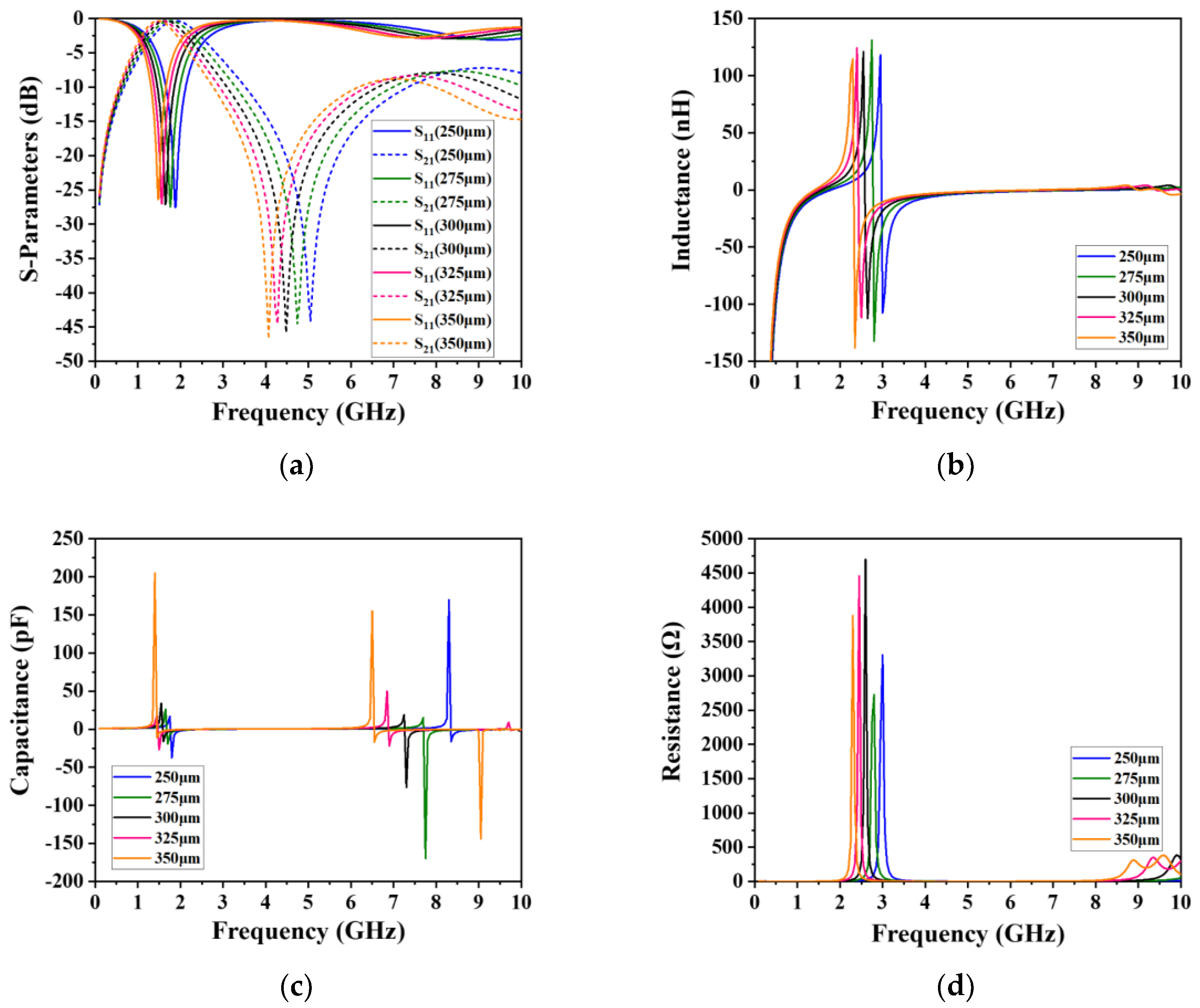
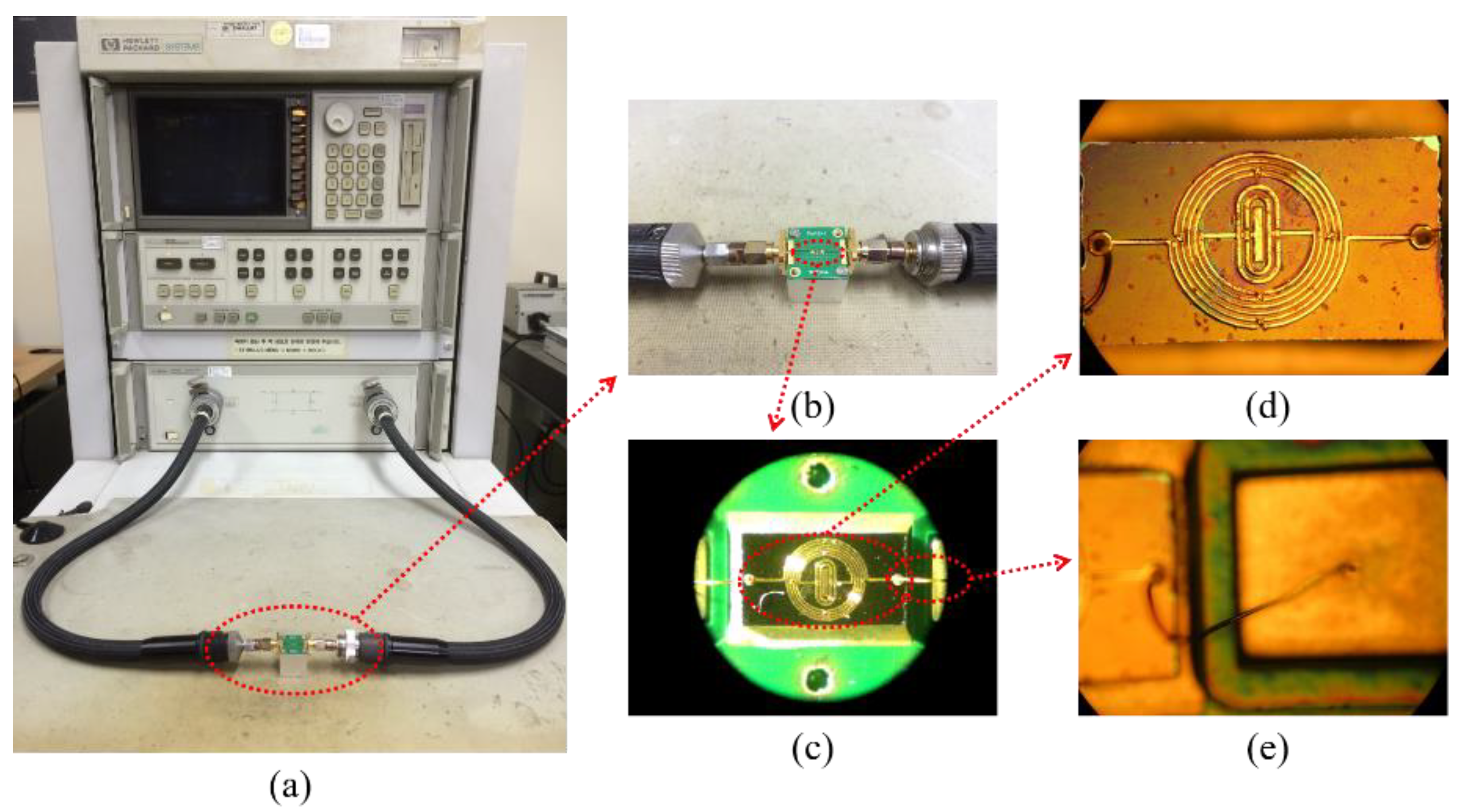
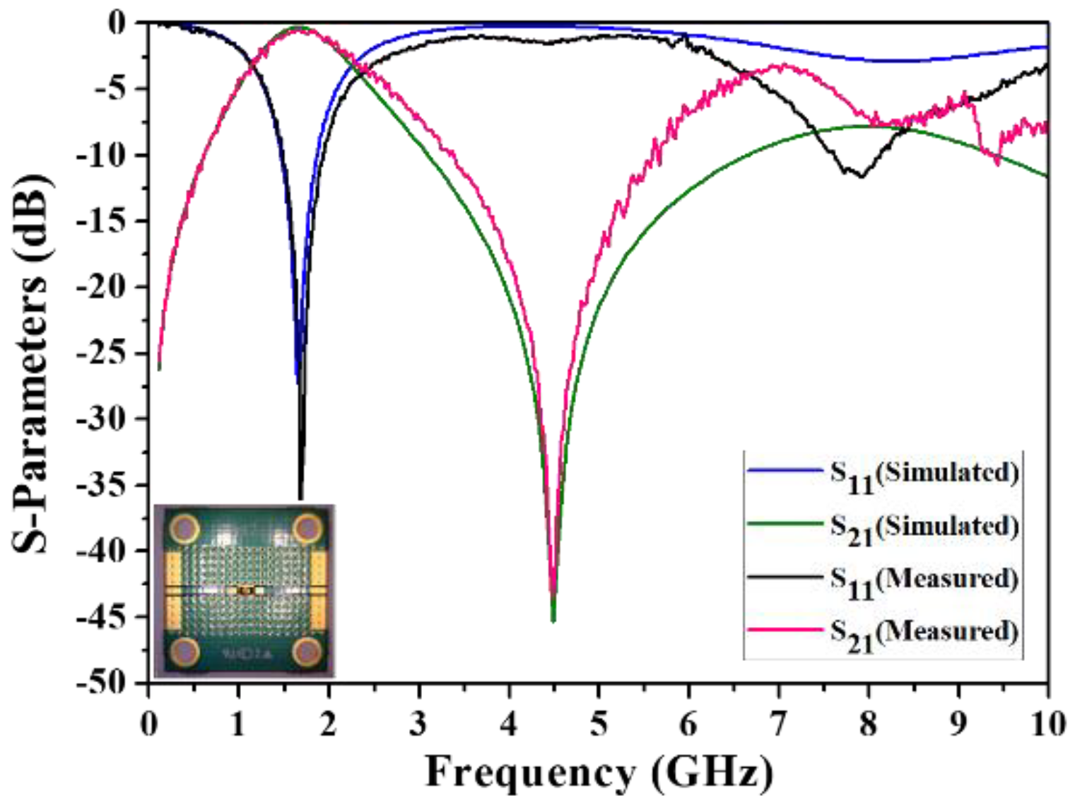
3. Results and Discussion

The influence of the inner radius of the outer inductor on performance was experimentally explored, as this parameter was varied from 250 μm to 350 μm in intervals of 25 μm. Figure 5 illustrates the variation of S-parameter and other lumped parameters as functions of BPF frequency and inner radius. Figure 5a indicates that the positions of the resonant mode and transmission zero tended to shift to areas of lower frequency in response to a larger inner radius. Because the inductance will increase with a bigger inner radius, thus, according to Equation (1), the bigger the inductance, the smaller the resonant frequency. It should also be noted that the impact on S21 is more prominent. According to Equations (2)–(4), there are many terms that need to be calculated; we therefore calculated them and tabulated them all in Table 4, which shows that the location of transmission zero definitely moves to areas of lower frequency with the increase of inner radius. Furthermore, inductance, capacitance, and resistance were derived based on the Y-parameters by using the following equations:
L ( nH ) = 1.0 × 10 9 × i m a g ( 1 Y ( 1 , 1 ) ) 2 π f
C ( pF ) = 1.0 × 10 12 2 π f × i m a g ( 1 Y ( 1 , 1 ) )
R ( Ω ) = r e a l ( 1 Y ( 1 , 1 ) )
where Y is the admittance, f is the frequency of operation, and imag and real represent the imaginary and real parts, respectively. As illustrated in Figure 5b–d, the first self-resonant frequency tended to decrease as the inner radius was increased. Furthermore, it was confirmed that, at high frequencies, the substrate capacitance reduced the self-resonant frequency (Figure 5c).
As previously mentioned, the proposed BPF was designed and simulated by using ADS software. In the design of the experimental BPF, the input and output ports were both connected to 50-Ω impedance-matching transmission lines of the PCB by golden wire bonding; the results were subsequently measured and recorded by using an Agilent 8510C vector network analyzer (VNA) (Agilent Technologies, Santa Clara, CA, USA). The experimental setup for the proposed BPF is illustrated in Figure 6 with enlarged views of various parts. The simulated and measured results for the BPF are depicted in Figure 7 along with photographs of the fabricated onboard chip. The results demonstrate that the proposed IPD BPF possesses a single passband with a central frequency of 1.71 GHz (return loss: 32.1 dB, insertion loss: 0.50 dB), and a wide FBW of 66.63%. One transmission zero with an amplitude of 43.42 dB was obtained on the right side of the passband at 4.48 GHz. The results of a comparison between the proposed IPD BPF and four previously developed IPD BPFs, as tabulated in Table 5, show that our device features a relatively small chip area and wide FBW.

4. Conclusions

In this paper, we reported on the design of an IPD technology-based BPF that was fabricated onto a gallium arsenide substrate, and was able to realize a small footprint, a wide FBW, a good out-band suppression, and high-frequency operational capability. The chip was fabricated onto a 6-in. gallium arsenide substrate with a dielectric constant of 12.85, loss tangent of 0.006, and thickness of 200.1 µm. Additionally, an equivalent circuit that considers the second-order parasitic effect was modeled in order to simulate device behavior under high-frequency operation. Furthermore, the current distributions were simulated for four different frequencies by using the 3D EM current simulator in ADS software. The influence of the geometric structure was also explored by varying the inner radius. The theoretical predictions and measurements performed on the fabricated bandpass filter were found to be in agreement, thus indicating that the proposed IPD BPF is a good candidate for RF/Microwave applications.

Author Contributions

Conceptualization, Z.-J.W. and T.Q.; Methodology, Z.-J.W.; Software, Z.-J.W.; Validation, Z.-J.W.; Formal Analysis, Z.-J.W.; Investigation, Z.-J.W.; Resources, Z.-J.W.; Data Curation, Z.-J.W.; Writing—Original Draft Preparation, Z.-J.W.; Writing—Review and Editing, E.-S.K., J.-G.L., and N.-Y.K.; Visualization, Z.-J.W.; Supervision, N.-Y.K.; Project Administration, E.-S.K. and N.-Y.K.; Funding Acquisition, N.-Y.K.

Funding

This research was supported by the basic research project conducted with support from the National Research Foundation of Korea (NRF) and the government (Ministry of Education) in 2018 (No. 2018R1A6A1A03025242), and a 2018 research grant from Kwangwoon University.

Conflicts of Interest

The authors declare no conflict of interest.

References

  1. Su, L.; Naqui, J.; Mata-Contreras, J.; Martin, F. Miniature microwave notch filters and comparators based on transmission lines loaded with stepped impedance resonators (SIRs). Micromachines 2015, 7, 1–10. [Google Scholar] [CrossRef]
  2. Liang, L.G.; Wang, C.; Kim, N.Y. Dual-band ultra-wideband bandpass filter with eight-resonant modes and quad-transmission zeros employing synchronous-quasi-resonance. Radioengineering 2017, 26, 713–720. [Google Scholar] [CrossRef]
  3. Liang, L.G.; Wang, C.; Kim, N.Y. Implementation of ultra-wideband bandpass filter with modularized design based on synchronous-quasi-resonance and double-curved-route. IET Microw. Antennas Propag. 2018. [Google Scholar] [CrossRef]
  4. White, J.F. High Frequency Techniques: An Introduction to RF and Microwave Design and Computer Simulation, 1st ed.; John Wiley & Sons: Hoboken, NJ, USA, 2004; pp. 335–398. ISBN 978-0-471-45591-2. [Google Scholar]
  5. Hong, J.S.; Lancaster, M.J. Microstrip Filters for RF/microwave Applications, 1st ed.; John Wiley & Sons: Hoboken, NJ, USA, 2001; pp. 1–6. ISBN 0-471-22161-9. [Google Scholar]
  6. Sebastian, M.T.; Jantunen, H. Low loss dielectric materials for LTCC applications: A review. Int. Mate. Rev. 2008, 53, 57–90. [Google Scholar] [CrossRef]
  7. Simon, R.W.; Hammond, R.B.; Berkowitz, S.J.; Willemsen, B.A. Superconducting microwave filter systems for cellular telephone base stations. Proc. IEEE 2004, 92, 1585–1596. [Google Scholar] [CrossRef]
  8. Yao, J.J. RF MEMS from a device perspective. J. Micromech. Microeng. 2000, 10, R9. [Google Scholar] [CrossRef]
  9. Kunze, M.; Heinrich, W. Hybrid dynamic-quasi-static finite-difference analysis of MMIC components with non-ideal conductivity. AEU-Int. J. Electron. Commun. 2003, 57, 137–146. [Google Scholar] [CrossRef]
  10. Bowick, C. RF Circuit Design, 2nd ed.; Elsevier: New York, NY, USA, 2007; pp. 37–62. ISBN 978-0-750-68518-4. [Google Scholar]
  11. Hsu, C.Y.; Chen, C.Y.; Chuang, H.R. A 77-GHz CMOS on-chip bandpass filter with balanced and unbalanced outputs. IEEE Electron Device Lett. 2010, 31, 1205–1207. [Google Scholar] [CrossRef]
  12. Yang, Y.; Zhu, H.; Zhu, X.; Xue, Q. A Low-loss bandpass filter using edge-coupled resonator with capacitive feeding in (Bi)-CMOS technology. IEEE Electron Device Lett. 2018, 39, 787–790. [Google Scholar] [CrossRef]
  13. Nan, L.; Mouthaan, K.; Xiong, Y.Z.; Shi, J.L.; Rustaagi, S.C.; Ooi, B.L. Design of 60-and 77-GHz narrow-bandpass filters in CMOS technology. IEEE Trans. Circuits Syst. 2008, 55, 738–742. [Google Scholar] [CrossRef]
  14. Pant, R.; Marpaung, D.; Kabakova, I.V.; Morrison, B.; Poulton, C.G.; Eggleton, B.J. On-chip stimulated Brillouin Scattering for microwave signal processing and generation. Laser Photon. Rev. 2014, 8, 653–666. [Google Scholar] [CrossRef]
  15. Zhang, W.; Minasian, R.A. Widely tunable single-passband microwave photonic filter based on stimulated Brillouin scattering. IEEE Photon. Technol. Lett. 2011, 23, 1775–1777. [Google Scholar] [CrossRef]
  16. Casas-Bedoya, A.; Morrison, B.; Pagani, M.; Marpaung, D.; Eggleton, B.J. Tunable narrowband microwave photonic filter created by stimulated Brillouin scattering from a silicon nanowire. Opt. Lett. 2015, 40, 4154–4157. [Google Scholar] [CrossRef] [PubMed] [Green Version]
  17. Chen, J.H. Enhancement of 5 GHz on-chip bandpass filter performance by using CMOS-MEMS inductors. Microsyst. Technol. 2018, 24, 2371–2377. [Google Scholar] [CrossRef]
  18. Jafari, B.; Sheikhaei, S. Pseudo-impulse tail current shaping for phase noise reduction in CMOS LC oscillators. Microelectron. J. 2018, 74, 60–68. [Google Scholar] [CrossRef]
  19. Jeon, H.; Kim, N.Y. A compact quadrature coupler on GaAs IPD process for LTE applications. IEICE Electron. Express 2013, 10, 20130386. [Google Scholar] [CrossRef]
  20. Wang, C.; Kim, N.Y. Analytical optimization of high-performance and high-yield spiral inductor in integrated passive device technology. Microelectron. J. 2012, 43, 176–181. [Google Scholar] [CrossRef]
  21. Li, Y.; Wang, C.; Kim, N.Y. A high performance compact Wilkinson power divider using GaAs-based optimized integrated passive device fabrication process for LTE application. Solid-State Electron. 2015, 103, 147–153. [Google Scholar] [CrossRef]
  22. Kim, E.S.; Kim, N.Y. Micro-fabricated resonator based on inscribing a meandered-line coupling capacitor in an air-bridged circular spiral inductor. Micromachines 2018, 9, 294. [Google Scholar] [CrossRef]
  23. Haobijam, G.; Palathinkal, R.P. Design and Analysis of Spiral Inductors, 1st ed.; Springer: New York, NY, USA, 2013; pp. 21–51. ISBN 978-81-322-1514-1. [Google Scholar]
  24. Choi, B.H.; Jin, Z.J.; Kim, M.G.; Sun, H.; Yun, T.Y. Equivalent-circuit model based on mathematical analysis for multilayer chip inductors. IET Microw. Antennas Propag. 2008, 2, 378–382. [Google Scholar] [CrossRef]
  25. Aryan, N.P. Design and Modeling of Inductors, Capacitors and Coplanar Waveguides at Tens of GHz Frequencies., 1st ed.; Springer: New York, NY, USA, 2014; pp. 19–34. ISBN 978-3-319-10187-3. [Google Scholar]
  26. Pakasiri, C.; Hsu, K.C.; Wang, S. Low-loss and highly-selective differential bandpass filter on integrated passive device process. Microw. Opt. Technol. Lett. 2018, 60, 970–975. [Google Scholar] [CrossRef]
  27. Sitaraman, S.; Sukumaran, V.; Pulugurtha, M.R.; Wu, Z.; Suzuki, Y.; Kim, Y.; Sundaram, V.; Kim, J.; Tummala, R.R. Miniaturized bandpass filters as ultrathin 3-D IPDs and embedded thinfilms in 3-D glass modules. IEEE Trans. Compon. Packag. Manuf. Technol. 2017, 7, 1410–1418. [Google Scholar] [CrossRef]
  28. Li, C.H.; Yu, M.C.; Lin, H.J. A compact 0.9-/2.6-GHz dual-band RF energy harvester using SiP technique. IEEE Microw. Wirel. Compon. Lett. 2017, 27, 666–668. [Google Scholar] [CrossRef]
  29. Wong, K.W.; Mansour, R.R.; Weale, G. Reconfigurable bandstop and bandpass filters with wideband balun using IPD technology for frequency agile applications. IEEE Trans. Compon. Packag. Manuf. Technol. 2017, 7, 610–620. [Google Scholar] [CrossRef]
Figure 1. Three-dimensional layout of the proposed bandpass filter (BPF), showing the three laminated layers (bottom to top: Bond layer, Text layer, Leads layer).
Micromachines 09 00463 g001
Figure 2. Configuration of the (a) Bond layer, (b) Text layer, and (c) Leads layer, and (d) a cross-sectional view of the fabricated integrated passive device (IPD) chip.
Micromachines 09 00463 g002
Figure 3. Equivalent circuit of the proposed BPF.
Micromachines 09 00463 g003
Figure 4. Simulated current density. (a) Frequency–current density illustration, and (b) Effects of 1.75 GHz on the simulated current density throughout the proposed BPF.
Micromachines 09 00463 g004
Figure 5. Simulated results illustrating the influence of the inner radius on the respective relationships between S-parameter and lumped parameters and frequency. (a) Simulated S-parameters, (b) simulated inductance, (c) simulated capacitance, and (d) simulated resistance.
Micromachines 09 00463 g005
Figure 6. S-parameter measurement setup for the proposed BPF. (a) Bandpass filter-vector network analyzer (VNA) cable connection; (b) a magnified view of the BPF and its input/output ports; (c) 50×-magnified top view of the BPF wire bonded to the printed circuit board (PCB); (d) a microscopic view of the fabricated onboard chip; (e) a microscopic view showing the BPF input-/output-port wire bond to the input/output pad.
Micromachines 09 00463 g006
Figure 7. Simulated and measured results for the proposed BPF.
Micromachines 09 00463 g007
Table 1. Dimensional parameters of the Bond layer.
Parameterabcdefrin
Unit (μm)20151178.597060258.7300
Table 2. Dimensional parameters of the Text layer.
Parameterabcdefrin
Unit (μm)16191174.596664254.7300
Table 3. Dimensional parameters of the Leads layer.
Parameterabcdefrin
Unit (μm)20151178.5970N/A258.7300
Table 4. Values and calculated results of the terms in Equations (2)–(4).
Terms ω mid (GHz) Ω c (GHz) ω 1 (GHz) ω 2 (GHz) ω 0 (GHz)FBW (%) w 0 (GHz)
250 μm2.0262.7491.3032.7491.89376.4015.066
275 μm1.9292.6251.2342.6251.80077.2334.703
300 μm1.8342.5191.1482.5191.70180.5814.474
325 μm1.7752.4511.0992.4511.64182.3974.315
350 μm1.6942.3521.0372.3521.56284.2324.063
Table 5. Comparison of IPD BPF performance.
ReferenceFabrication ProcessCircuit Area (mm2)Passband (GHz)Fractional Bandwidth (%)
[26]Si-IPD3.742.2073.00 (3-dB)
[27]Glass-IPD<1.002.6049.62 (3-dB)
[28]Si-IPD11.60.9/2.6N/A
[29]Si-IPD3.91.716 (10-dB)
This workGaAs-IPD1.141.7166.63 (3-dB)

