
Progress of MEMS Scanning Micromirrors for Optical Bio-Imaging

Electrical Engineering Department, University of Washington, Seattle, WA 98195-2500, USA
*
Author to whom correspondence should be addressed.
Micromachines 2015, 6(11), 1675-1689; https://doi.org/10.3390/mi6111450
Submission received: 16 September 2015
/
Revised: 17 October 2015
/
Accepted: 28 October 2015
/
Published: 5 November 2015
(This article belongs to the Special Issue Optical Microsystems)
Abstract
:Microelectromechanical systems (MEMS) have an unmatched ability to incorporate numerous functionalities into ultra-compact devices, and due to their versatility and miniaturization, MEMS have become an important cornerstone in biomedical and endoscopic imaging research. To incorporate MEMS into such applications, it is critical to understand underlying architectures involving choices in actuation mechanism, including the more common electrothermal, electrostatic, electromagnetic, and piezoelectric approaches, reviewed in this paper. Each has benefits and tradeoffs and is better suited for particular applications or imaging schemes due to achievable scan ranges, power requirements, speed, and size. Many of these characteristics are fabrication-process dependent, and this paper discusses various fabrication flows developed to integrate additional optical functionality beyond simple lateral scanning, enabling dynamic control of the focus or mirror surface. Out of this provided MEMS flexibility arises some challenges when obtaining high resolution images: due to scanning non-linearities, calibration of MEMS scanners may become critical, and inherent image artifacts or distortions during scanning can degrade image quality. Several reviewed methods and algorithms have been proposed to address these complications from MEMS scanning. Given their impact and promise, great effort and progress have been made toward integrating MEMS and biomedical imaging.
1. Introduction
Advanced optical imaging technologies such as scanning confocal microscopy [1], optical coherence tomography (OCT) [2], and multiphoton microscopy [3,4] have become important diagnostic tools in biomedicine. They are non-invasive and capable of in vivo assessment of tissue microanatomy below the epithelial surface in real time at resolutions (~0.5–10 μm) approaching those of conventional histological techniques, and combining these technologies with endoscopy further enables high-resolution optical imaging of internal organs [5]. Advancements in these optical imaging technologies have made substantial impacts in early detection, diagnosis, and treatment of diseases.
All these imaging techniques require mechanisms to deliver, focus, scan, and collect a single-mode optical beam. Although it is possible to achieve this using a single-mode optical fiber as the scanning catheter [6,7,8], most fiber-imaging approaches require resonant scanning in order to generate sufficient deflection for a reasonable field of view, thereby limiting the types of employable scan patterns.
Due to the capability of integrating complex functionality in small devices, microelectromechanical systems (MEMS) technologies have been explored to develop scanning devices for endoscopic imaging. MEMS scanning mirrors can perform large angle scanning without resonance, which enables arbitrary scan patterns. Their versatility further allows operation at resonance to achieve high-speed raster scanning, which is necessary for real-time en face imaging. Various MEMS scanning mirrors have been developed for beam steering in confocal microscopy [9,10,11,12,13,14], OCT [15,16,17,18,19,20,21], and two-photon microscopy [22]. In these micromirrors, 2D scanning motions can derive from thermoelectric, electrostatic, electromagnetic, or piezoelectric actuation, and the microfabrication adaptability of MEMS devices facilitates integration of additional functionality such as adjustable-focal-length scanning micromirrors [23] or dynamic aberration correction [24]. Varifocal MEMS micromirrors have demonstrated improvement in lateral image resolution without compromising the depth of focus [25,26], and they can also enable dynamic focus tracking in OCT imaging [27].
Although MEMS scanning micromirrors have also been developed for other applications such as optical communications and laser beam scanning, the focus of this review is on works specifically applied to biomedical imaging. In Section 2, we discuss various scanning micromirror technologies based on their actuation mechanisms; in Section 3, we discuss the efforts that have been made to correct and improve the images acquired by optical systems utilizing MEMS scanning mirrors; and in Section 4, we summarize the pros and cons of different scanning micromirror technologies and conclude the paper.
2. Scanning Micromirror Technologies
Various actuation mechanisms have been developed to achieve 2D scanning functionality for MEMS mirrors. The predominant approaches are thermoelectric, electrostatic, electromagnetic, and piezoelectric actuation, with each possessing advantages and disadvantages in various imaging modalities. In this section, we describe the basic principle of each technology and review the progress each has made.
2.1. Thermoelectric Actuation
Thermoelectric actuation typically involves thin bimorph actuation structures that utilize contrasting thermal expansion coefficients between the constituent materials. The actuation mechanism was first applied to a MEMS scanning micromirror fabricated on single-crystal silicon using a deep reactive-ion etch (DRIE) after complementary metal-oxide-semiconductor (CMOS) micromachining for OCT imaging [28]. In this work, the fabricated micromirror has a thermal actuation structure consisting of a multi-layer Al/oxide mesh and an integrated polysilicon heater, and the actuator connects one edge of the MEMS micromirror to the substrate. The mesh curls up after release of the micromirror structure due to the tensile stress in the Al layer and the compressive residual stress in the bottom SiO2 layer. Upon heating the actuator by driving an electric current through the polysilicon heater, the micromirror tilts back towards the substrate, thus achieving scanning motion. The micromirror achieved 17° of rotation under 15 mA of applied direct current (DC), and the 1 mm × 1 mm micromirror has a resonance frequency of 165 Hz. It was packaged in a 5 mm-diameter catheter tip for an endoscopic OCT system and applied to in vivo imaging of a porcine urinary bladder through cystotomy. An image resolution of 20 μm was achieved.
A similar micromirror was later applied to two-photon fluorescence and second-harmonic generation endoscopy by combining with a double-clad photonic crystal fiber, and the system was used for rat esophagus imaging [29]. In order to achieve two-dimensional scanning necessary for obtaining 3D volumetric images in OCT, a similar structure was designed and demonstrated instead with thermoelectric-bimorph beams that enabled an added rotation axis, as shown in Figure 1 [20]. The micromirror achieved a 40° rotation angle under ~6.3 mA applied current, and resonant frequencies of 445 and 259 Hz for the two scanning directions.
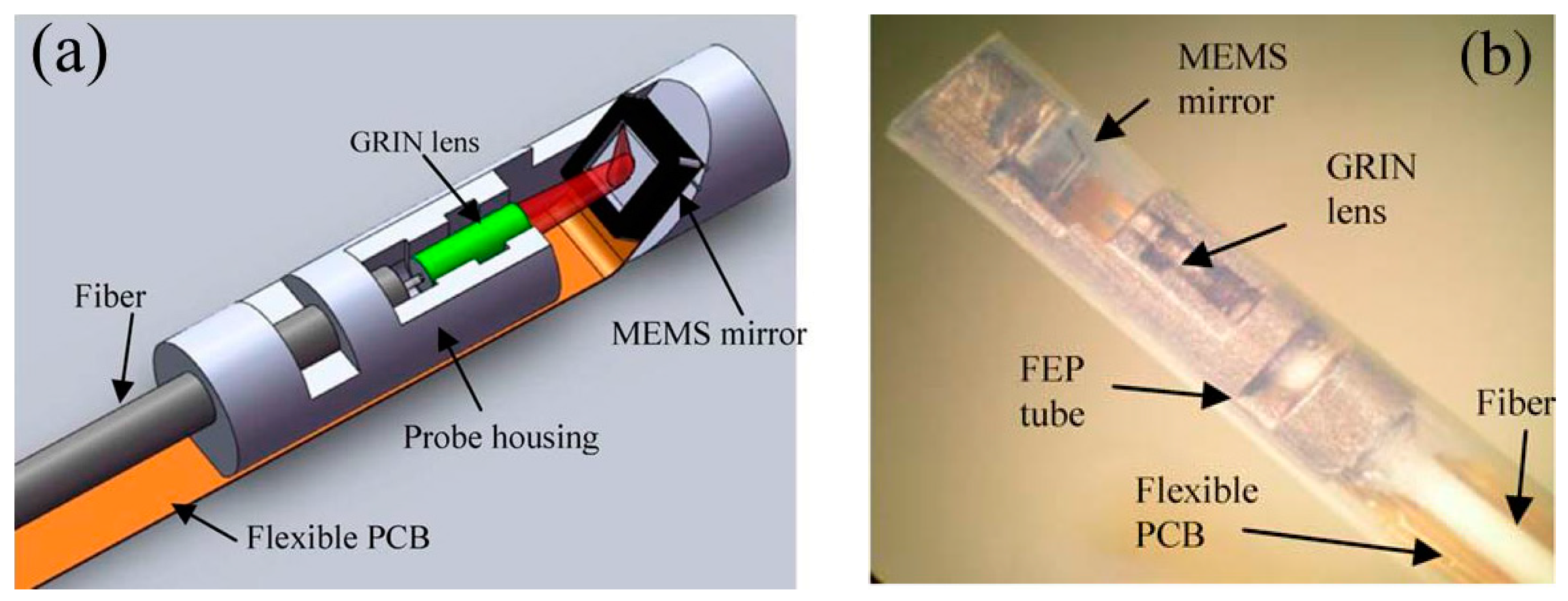
Previous thermoelectric-actuated micromirrors had rotation axes about the edges of the mirror, which may pose complications for optical system design and alignment due to the lateral shift of the optical path accompanying rotation. Modifications to the thermoelectric-bimorph structures can overcome this limitation by anchoring at the center of the mirror edges, as shown in Figure 2 [21]. In order to increase the tilting angles of the micromirror, a folded architecture was designed for the thermoelectric bimorphs. The micromirror achieved ±15° of rotation under 5.5 V/15 mA of actuation voltage/current, and a resonant frequency of 400 Hz. The micromirror was packaged into an imaging probe for OCT with an outer diameter of 5.8 mm. With a new hidden actuator design, the die size was further reduced, yielding an OCT probe with a 2.8 mm diameter [30]. Figure 3 shows the packaging design and a photograph of the probe. The new thermoelectric-actuated micromirror achieved ±11.5° of rotation angle under 4.8 V of applied voltage, and a 406 Hz resonant frequency.
Figure 1.
Scanning-electron microscopy (SEM) image of a 2D thermoelectric-actuated scanning micromirror [20]. Reproduced with permission from Xie, H., Journal of Selected Topics in Quantum Electronics; published by IEEE, 2004.
Figure 1.
Scanning-electron microscopy (SEM) image of a 2D thermoelectric-actuated scanning micromirror [20]. Reproduced with permission from Xie, H., Journal of Selected Topics in Quantum Electronics; published by IEEE, 2004.
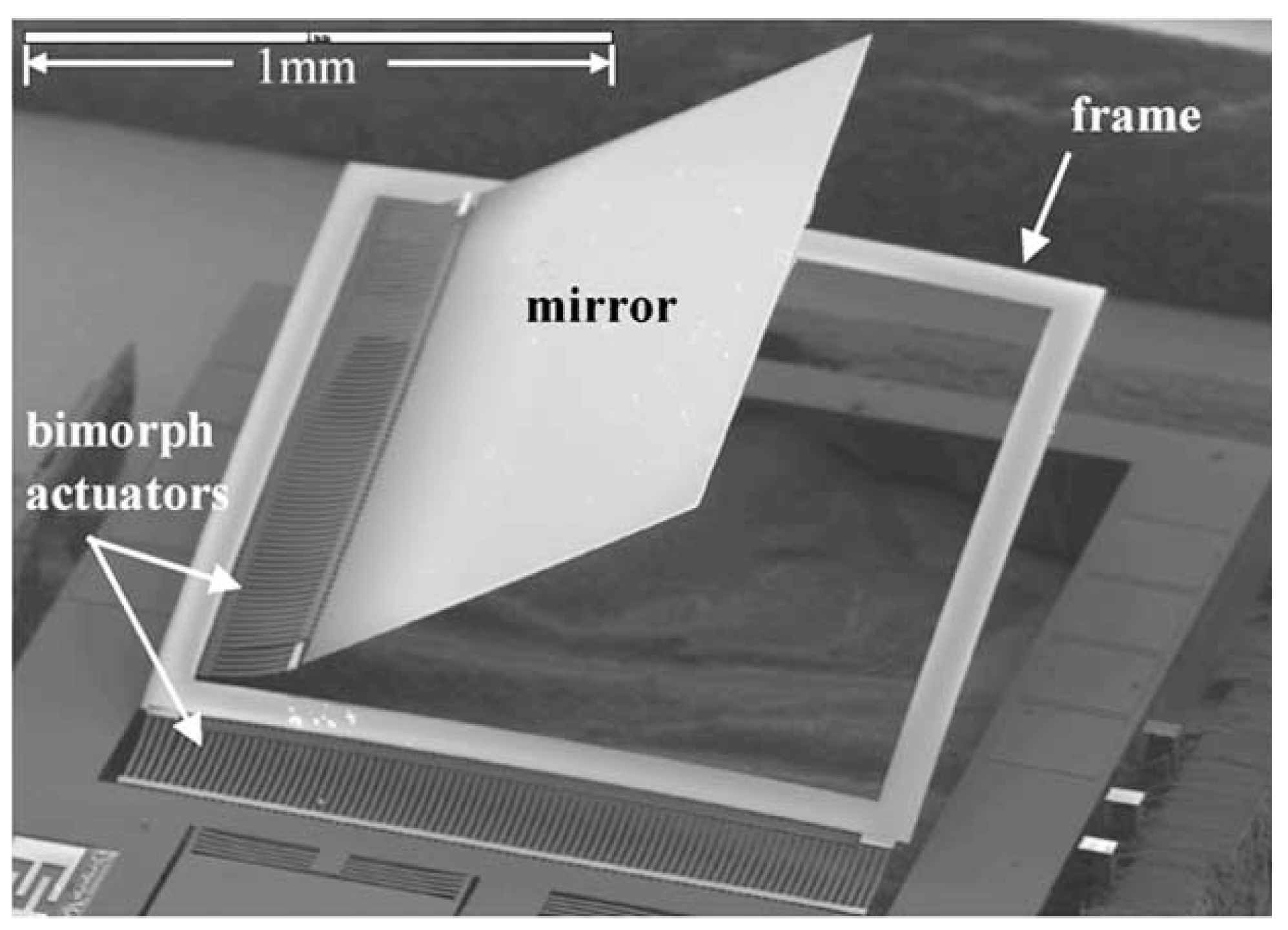
Figure 2.
(a) SEM image of a 2D thermoelectric-actuated scanning micromirror with rotation axes about the center; (b) and (c) Close-up SEM images of the folded thermoelectric-bimorph structure [21]. Reproduced with permission from Xie, H., Optics Express; published by OSA Publishing, 2010.
Figure 2.
(a) SEM image of a 2D thermoelectric-actuated scanning micromirror with rotation axes about the center; (b) and (c) Close-up SEM images of the folded thermoelectric-bimorph structure [21]. Reproduced with permission from Xie, H., Optics Express; published by OSA Publishing, 2010.
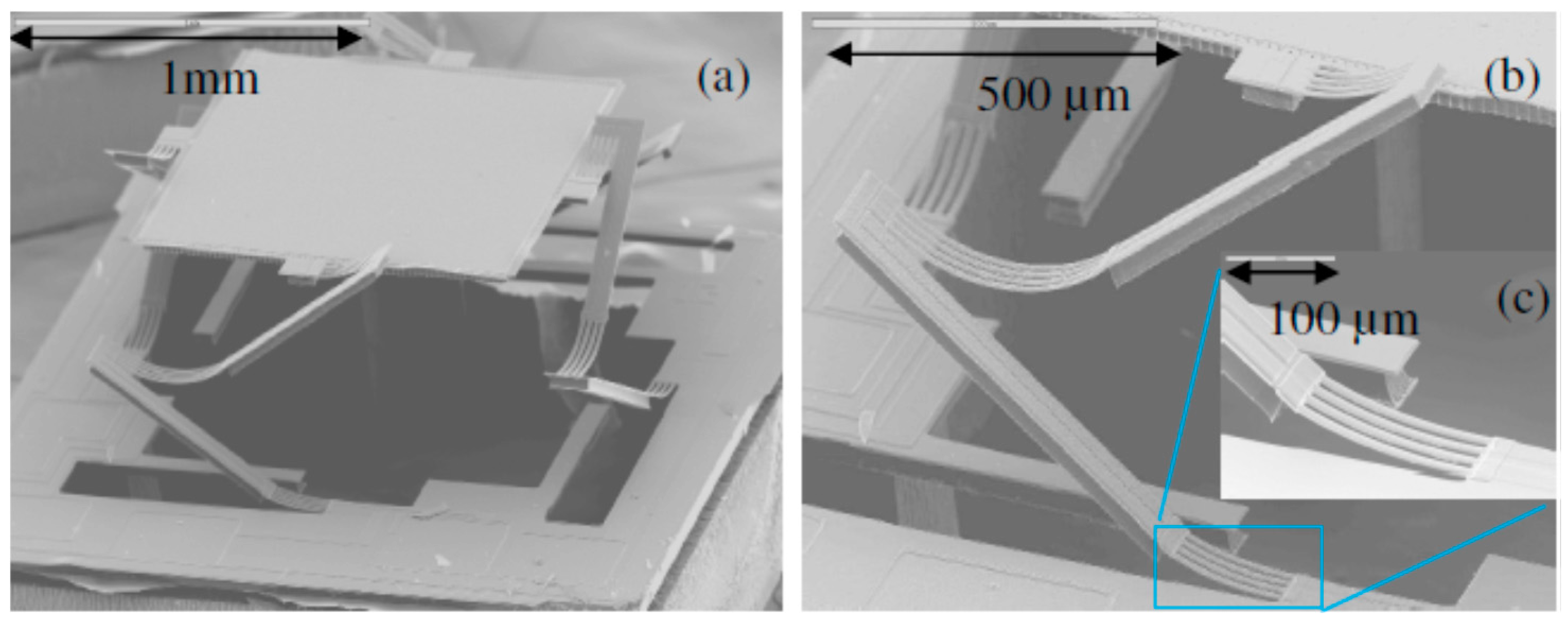
Figure 3.
(a) Package design of an optical coherence tomography (OCT) probe employing a thermoelectric-actuated scanning micromirror with hidden actuators, a graded-index (GRIN) lens, a flexible printed circuit board (PCB), and a fluorinated ethylene propylene (FEP) tube for protection; (b) Photograph of the packaged OCT probe depicted in (a) [30]. Reproduced with permission from Xie, H., Journal of Microelectromechanical Systems; published by IEEE, 2012.
The thermoelectric-bimorph structure can also actuate a platform vertically. By opening a hole in the platform for placing a lens, a movable lens can be realized to achieve focus depth scanning. Combining this with the two-axis scanning micromirror, a confocal microscope was demonstrated. The system achieved a ±26° optical scan range (corresponding to ±13° mechanical rotation angle) and over 400 μm in depth scan range. The lateral resolution and axial resolution were characterized to be 1.0 μm and 7.0 μm, respectively [14].
Thermoelectric-bimorph membranes can achieve tunable focal lengths for MEMS mirrors, and the radius of curvature of a gold-coated micromirror was tuned from 2.5 to 8.2 mm over a current-induced temperature range from 22 to 72 °C [31]. More recently, such a capability was combined with thermoelectric scanning actuation to achieve a tip-tilt-piston, varifocal micromirror [23], shown in Figure 4. Four bimorphs are positioned tangentially at the micromirror edges to suspend it above the substrate upon release. As shown in the zoom-in SEM image of Figure 4b, each of the four bimorph legs is connected at the tip to a polysilicon serpentine spring. Bending, twisting, and extension of the springs allow tilting of the micromirror, and actuating all four bimorph legs simultaneously at the same power provides piston motion. The 400 μm-diameter mirror surface is separated into eight polysilicon/gold bimorph wedges. The springs also serve as local heaters for these bimorph wedges to achieve a tunable radius-of-curvature. By applying a current between any of the two legs, the serpentine springs can be heated. The micromirror was able to achieve a mechanical tilt angle of ±20° with a total power of 90 mW, a tunable focal length of −0.48 to +20.5 mm with a total power of 27 mW, and a piston motion range of 300 μm. Degradation of mirror reflectivity due to the release holes on the micromirror surface was characterized to be 14%. The thermal actuation response time is ~5 ms for large angles. Although not specifically designed for biomedical imaging, the mirror size and frequency response may be further optimized for such applications.
Figure 4.
SEM images of a thermoelectric varifocal MEMS scanning micromirror. (a) The four bimorph actuators provide piston and tilting motion; (b) Zoom-in of the device: the top of the four bimorph legs are connected to the micromirror through four serpentine springs, which allow for tilting the micromirror and heating the mirror wedges to adjust the focal length [23]. Reproduced with permission from Bishop, D., Optics Express; published by OSA Publishing, 2015.

In addition to the previously described processes, a thermoelectric-actuated scanning micromirror has also been designed and fabricated using a silicon-on-insulator (SOI) MEMS process for endoscopic bioimaging [32]. The micromirror achieved a maximum angular tilt of 17° with 36.8 mW of actuation power. The minimum chip size designed was 1 mm × 1 mm with a 400 μm-diameter mirror plate.
2.2. Electrostatic Actuation
The electrostatic actuation mechanism is attractive for MEMS scanning micromirrors because the capacitive actuators draw very little current, therefore requiring low operating power despite the need for large applied voltages. Two main approaches, comb-drive and parallel-plate gap-closing schemes, have been widely explored for electrostatic actuation, and in this section, we discuss MEMS scanning micromirrors based on these two approaches.
2.2.1. Comb-Drive Actuation
Comb-drive actuated, scanning micromirrors have been demonstrated for OCT [16], OCT endoscopy [19,33], swept-source OCT [34], confocal microscopy [35,36], a near-infrared confocal microscope [37], two-photon fluorescence imaging [22], near-infrared fluorescence confocal imaging [12], and confocal endoscopy [38]. Typically, vertical comb-drive actuators are employed, which consist of comb structures initially vertically offset from each other. Upon applying a voltage, the electrostatic force pulls the movable comb up or down to align with the fixed comb, causing tilting of the micromirror. Compared to the gap-closing electrostatic actuation mechanism to be described in the next section, vertical comb-drive actuation can achieve a linear relationship between the mirror-tilting angle versus applied voltage. The actuators normally occupy substantial chip areas, which is the main drawback of this approach.
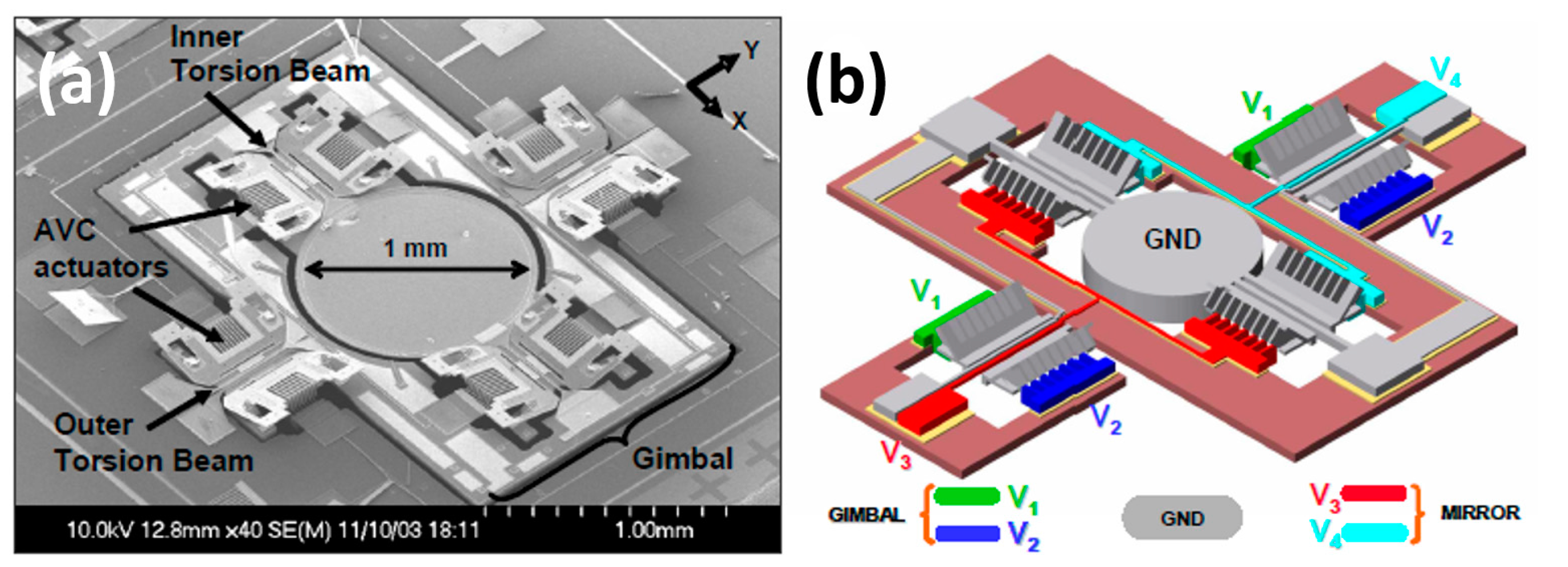
A MEMS scanning mirror utilizing angular vertical-comb (AVC) actuators was demonstrated for endoscopic OCT and reported in [19], and Figure 5 shows a SEM image and a schematic drawing of the device. The angular vertical-comb actuator can achieve larger scan angles for the same comb dimensions compared to standard vertical comb actuators. The device was fabricated by integrating surface and bulk micromachining processes to produce a micromirror having a diameter of 1 mm and a complete scanner area measuring 3 mm × 3 mm. As described earlier, electrostatic actuation serves as a capacitive load and draws very little current for low frequency actuation, in general less than 1–10 nA. The device was packaged with an achromatic lens (f = 10 mm) and a fiber collimator to realize an OCT catheter with diameter = 5 mm. The micromirror was mounted at 45° to the optical path; therefore, the OCT catheter captured side views with a working distance of ~2 mm. The non-resonant mechanical scanning angle was measured to be ±6° at >100 V bias, while operating under resonance [resonant frequencies = 463 Hz (for the inner axis) and 140 Hz (for the outer axis)] is expected to significantly increase the scanning angle. The MEMS OCT catheter was incorporated into an ultrahigh resolution OCT imaging system, and with all focusing optics optimized, the system achieved a transverse resolution of ~12 μm. The system was used for in vivo imaging of human skin and in vitro imaging of lime pulp and a hamster cheek pouch, achieving an imaging rate of 4 frames/s over a three-dimensional field of view measuring 1.8 mm × 1.0 mm × 1.3 mm corresponding to 500 × 500 × 1000 pixels.
Figure 5.
A microelectromechanical systems (MEMS) scanning micromirror with angled vertical-comb actuators. (a) SEM image; (b) Schematic drawing of the device [19]. Reproduced with permission from Wu, M. C., Optics Express; published by OSA Publishing, 2007.
Figure 5.
A microelectromechanical systems (MEMS) scanning micromirror with angled vertical-comb actuators. (a) SEM image; (b) Schematic drawing of the device [19]. Reproduced with permission from Wu, M. C., Optics Express; published by OSA Publishing, 2007.
The OCT catheter was also demonstrated using a MEMS scanning mirror comprised of conventional vertical comb-drive actuators fabricated on single-crystal silicon [33]. The diameter of the MEMS mirror was 1.2 mm, and the packaged catheter diameter was 4 mm. The micromirror achieved ±5° of mechanical scanning angle under 100 V bias. Due to the use of single-crystal silicon, the resonant frequencies were higher, measured at 2.4 and 1.8 kHz for the inner and outer axes. Volume images were obtained at a rate of 3 frames/s, with a three-dimensional field of view of 1.0 mm × 1.0 mm × 1.4 mm containing 400 × 200 × 560 pixels. When incorporated with spectral domain or swept-source OCT systems [34], higher frame rates can be achieved while using the MEMS scanning mirror catheter.
In conventional confocal microscopy, the axial resolution is determined by the numerical aperture (NA) of the focused beam. For high-resolution imaging, a large NA is required which leads to a short working distance. A dual-axes confocal microscope can overcome this limit [39] by utilizing two low-NA beams intersecting at a small focal volume for both illumination and light collection. The dual-axes confocal configuration can achieve higher axial resolution without compromising transverse resolution, and the long working distance enables post-object scanning, leading to a larger field-of-view with less aberrations. A MEMS double-mirror scanner was proposed and demonstrated to enable packaging of a dual-axes confocal microscope in a compact configuration [35,37]. Figure 6 shows a SEM image and a cross-sectional view of the various structures of the scanner. The scanner consists of two reflective mirror surfaces actuated simultaneously by self-aligned vertical comb-drives and is fabricated on a double SOI wafer, producing mirror surfaces each measuring 650 × 600 μm. The demonstrated maximum mechanical tilting angles in static mode are ±2.4° at 160 V for the outer axis and ±2.75° at 170 V for the inner axis. The resonant frequencies are at 500 and 2.9 kHz for the outer and inner axes, respectively, leading to an imaging frame rate of 8 frames/s. When operated under resonance, the micromirror achieves mechanical tilting angles of ±6.2° and ±3.6° for the outer and inner axes, respectively.
Figure 6.
A MEMS double-mirror scanner for dual-axes confocal microscopy. (a) SEM image; (b) Cross-sectional view of the various structures of the scanner [35]. Reproduced with permission from Solgaard, O., Journal of Microelectromechanical Systems; published by IEEE, 2007.
Figure 6.
A MEMS double-mirror scanner for dual-axes confocal microscopy. (a) SEM image; (b) Cross-sectional view of the various structures of the scanner [35]. Reproduced with permission from Solgaard, O., Journal of Microelectromechanical Systems; published by IEEE, 2007.

The dimensions of the MEMS chip are 3.4 mm × 2.9 mm, appropriate for packaging in a dual-axes confocal microendoscope scan head with a configuration as shown in Figure 7a [13]. Figure 7b shows a photograph of the 5.5 mm-diameter scan head without its cap, revealing the MEMS double-mirror scanner. Confocal imaging can be performed in either reflectance or fluorescence mode. The confocal images have a field-of-view of 362 μm × 212 μm containing 500 × 295 pixels. The transverse resolution of the images is 5 μm, while the axial resolution is 6.5 μm. The handheld dual-axis confocal microendoscope was used to successfully obtain ex vivo fluorescence images of excised tissue specimens from normal and dysplastic colonic mucosa, as well as in vivo fluorescence images in the colons of human patients. An improved split-frame configuration reduces the chip size of the MEMS dual-mirror scanner to 1.8 mm × 1.8 mm [40].
Figure 7.
A dual-axes confocal microendoscope scan head containing a MEMS double-mirror scanner. (a) The schematic drawing of the package. Two collimated beams are focused by a parabolic mirror with a 5 mm diameter and numerical aperture NA = 0.5. En face scanning is achieved by the MEMS micromirror scanner enclosed in a 5.5 mm scan head; (b) Photograph of the scan head without its cap, showing the MEMS scanner mounted on an axial translation stage [13]. Reproduced with permission from Solgaard, O., Journal of Biomedical Optics; published by SPIE, 2012.

2.2.2. Gap-Closing Actuation
Gap-closing actuation utilizes electrostatic attraction between two parallel structures: one is the scanning micromirror and the other is a bottom electrode. Since the electrodes are underneath the micromirror, this actuation mechanism can enable smaller overall die size. The relationship between mirror tilting angle and the applied voltage is not linear under DC actuation, therefore calibration is required in order to avoid image distortion.
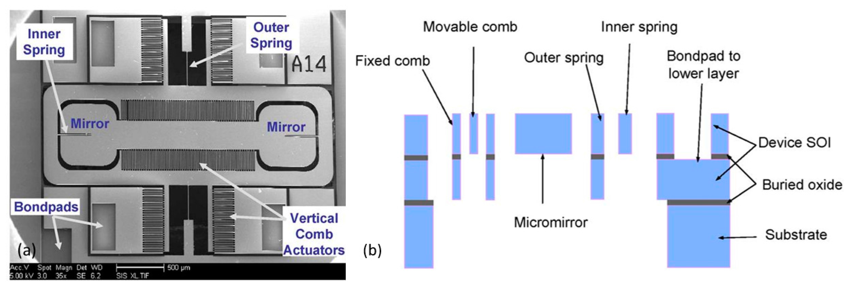
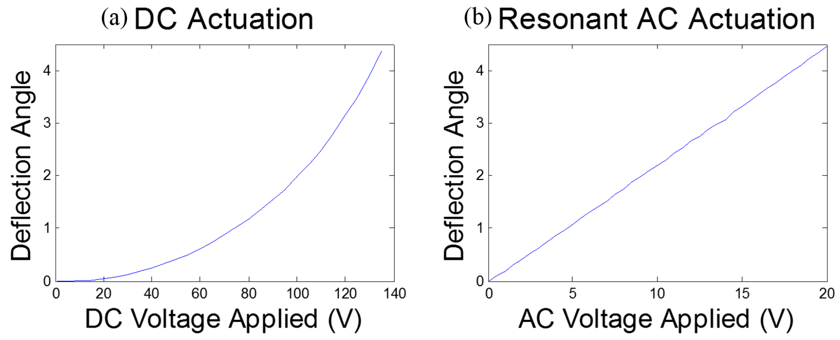
A 1D MEMS scanning micromirror using gap-closing actuation was first employed in a confocal optical microscope, with 2D scanning achieved through incorporating two micromirrors scanning in orthogonal directions [10]. By employing quad-electrodes, 2D scanning can be integrated in one micromirror, and these devices have been applied in OCT imaging [9,18,41]. Figure 8 shows the SOI-based fabrication process and a top-view optical microscope image of such a device [18] where the MEMS micromirror employs a biaxial gimbal structure allowing 2D scanning of the mirror. The fabrication is based on SOI processes. It involves patterning and etching the micromirror, springs, and gimbal structures in the active Si layer; etching a backside window though the Si handle wafer down to the buried oxide layer; and then releasing the structure by removing the oxide layer. The backside window also allows for alignment with another Si wafer containing quad-electrode pedestals, which is not shown in the figure. Figure 9 plots the scanning performance of the device: static actuation results in a typical non-linear mechanical deflection versus applied voltage curve for gap-closing electrostatic actuated devices (Figure 9a), while the result is linear under resonant actuation (Figure 9b). Under DC actuation, the micromirror achieved a mechanical deflection angle greater than ±4° with 130 V bias. The same deflection angle could be achieved with less than 20 V alternating-current (AC) bias under resonance if a constant DC 60 V bias is applied. The DC bias ensured that the voltage applied to the mirror was always greater than zero and had the added benefit of reducing the AC voltage necessary for resonant scanning. The resonant frequencies are 472 and 399 Hz for the inner and outer axes, respectively. The MEMS scanning mirror was employed in an OCT system and images of a mouse ear were obtained successfully.
The capability of focus-tracking allows scanning through a substantial range in the depth direction with high transverse resolution. Dynamic focus control was first demonstrated as a separate function in MEMS micromirrors using electrostatic attraction between the mirror membrane and an underlying frame. MEMS micromirrors with adjustable focus have been incorporated in a 1D OCT system [25], Doppler OCT [17], endoscopic confocal and OCT imaging [24], and a laser scanner when combined with a 1D or 2D scanning micromirror [42]. Figure 10 shows the cross-sectional view and a top-view microscope image of such a device [24]. The deformable micromirror membrane is fabricated on a layer of silicon nitride, and a layer of silicon dioxide is sandwiched between the nitride membrane and the Si wafer as the sacrificial layer. The sacrificial oxide release creates the initial air gap, and the final cavity depth is formed by an anisotropic wet etch of the (100) Si. The achieved focus scan range was 1.25 mm under 200 V bias [25].
A focus-adjustable silicon nitride mirror membrane can be fabricated on top of a 2D gimbal MEMS scanning mirror to achieve an integrated 3D scanning device [27,43]. The devices reported in reference [27,43] have similar structures, but different fabrication processes and mirror geometries. Figure 11 shows the fabrication process reported in reference [27], and a SEM image of the device is shown in Figure 12a. The thicknesses of the mirror and the gimbal for the finished devices are ~20 μm, and the cavity beneath the mirror is ~4 μm deep. While the thickness of the device tethers was defined by the silicon nitride thickness (500 nm), width variations of the tethers between 10 and 40 μm allowed slight device tunability. The electrode pillars were fabricated utilizing anisotropic KOH etching of a Si wafer. An optical-microscopy image of the electrode pillar is shown in Figure 12b. The final device is assembled by aligning and inserting the pillar into the cavity under the micromirror device (Figure 11f).
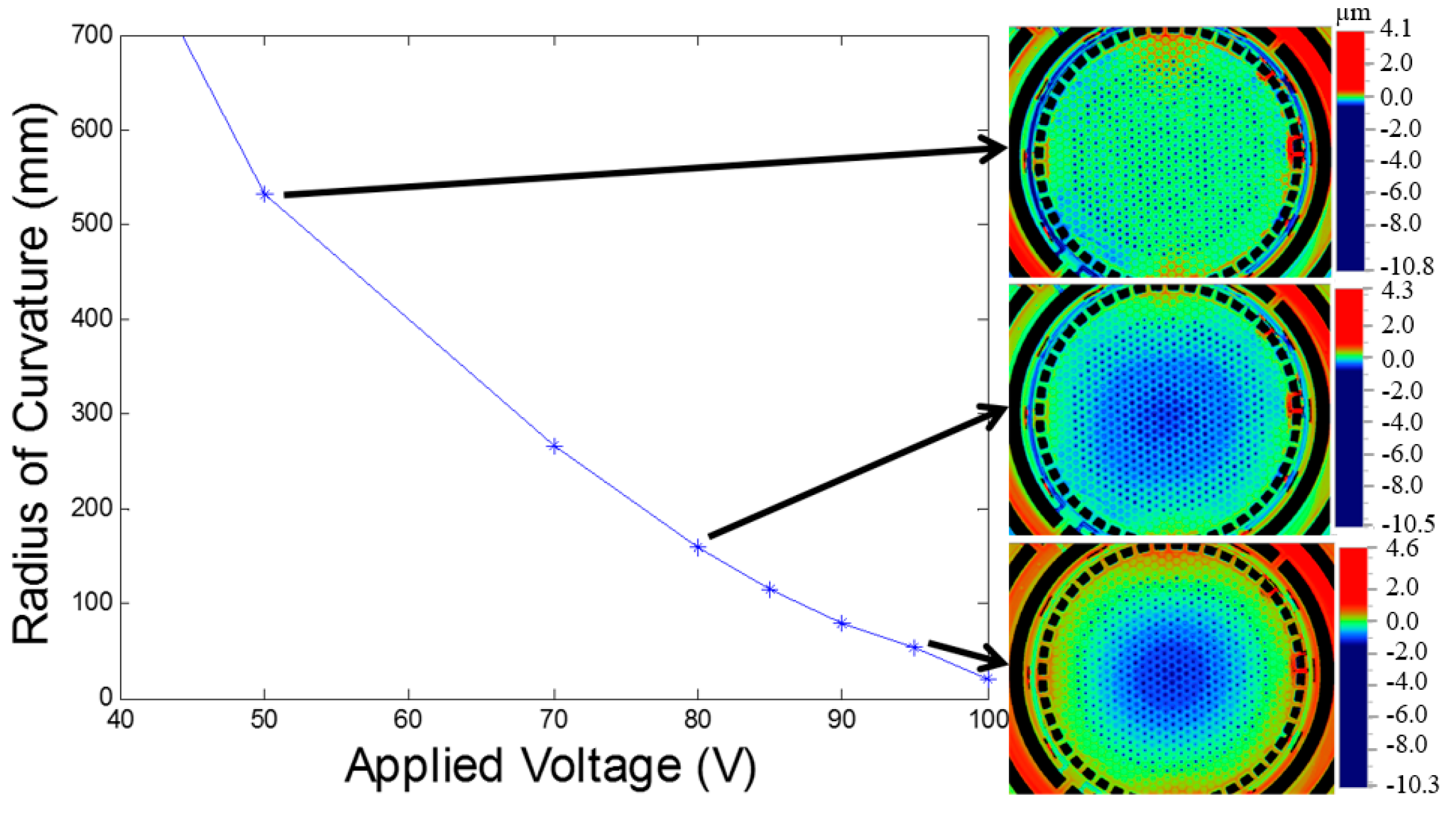
The mechanical resonant frequency of the 3D MEMS scanning mirror was measured to be ~216 Hz. Softer tethers made of silicon nitride resulted in the reduced resonant frequency. The micromirror demonstrated a ±5° mechanical tilting angle at 140 V bias under DC actuation, and greater than ±4° tilting angle at 40 V under resonant AC actuation. Focus control was characterized using an optical surface profiler while applying a voltage between the mirror membrane and the Si frame underneath. As shown in Figure 13, between 50 and 95 V, the membrane exhibits significant deflection of the mirror’s center indicated by the dark blue color. A large focus-control range was achieved with the radius-of-curvature tunable from infinity to 50 mm with <100 V actuation. It was also observed that the deflection is uniformly distributed across the mirror which is important for high optical beam quality. Beam profile characterization of a reflected laser beam by the deformed micromirror showed good fitting to a Gaussian beam and confirmed that the optical beam was not distorted by the mirror membrane. When the optical system includes an additional focusing lens with a NA of 0.85, it can achieve a focus spot size as little as 5 μm. While this additional lens decreases the focused spot size, the achievable range of focal length control for the system is also decreased and needs to be considered in designing the overall optical system.
Figure 8.
A 2D MEMS scanning micromirror. (a) Fabrication process: A, A double-side polished SOI wafer is shown. B, Plasma-enhanced chemical-vapor deposition (PECVD) is used to deposit conformal silicon nitride on both sides of the wafer, and the backside is patterned. C, The backside of the wafer is etched with potassium hydroxide (KOH) to the silicon oxide stop layer in the location of the mirrors. D, Phosphoric acid at 160 °C is used to remove the silicon nitride, and a layer of gold is deposited for the reflective mirror surface. E, Metal and silicon trenches are etched down to the oxide layer. F, Hydrofluoric acid (HF) is used to finish the release of the device; (b) Top-view optical microscope image of a gold-coated micromirror [18]. Reproduced with permission from Lin, L.Y., Biomedical Optics Express; published by OSA Publishing, 2015.
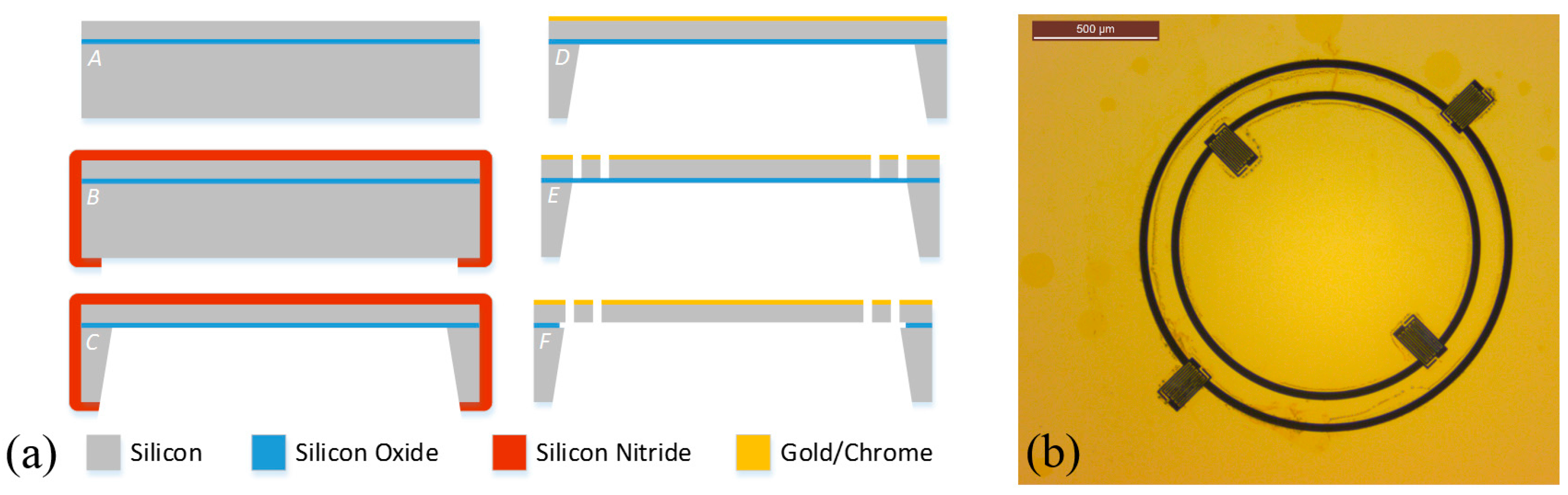
Figure 9.
The mechanical deflection angle of a 2D MEMS scanning micromirror using gap-closing electrostatic actuation. (a) DC actuation; (b) Resonant AC actuation with a constant 60 V DC bias. Reproduced with permission from Lin, L.Y., Biomedical Optics Express; published by OSA Publishing, 2015.
Figure 9.
The mechanical deflection angle of a 2D MEMS scanning micromirror using gap-closing electrostatic actuation. (a) DC actuation; (b) Resonant AC actuation with a constant 60 V DC bias. Reproduced with permission from Lin, L.Y., Biomedical Optics Express; published by OSA Publishing, 2015.

Figure 10.
A MEMS mirror with adjustable focus. (a) Cross-sectional view of the device, illustrating a two-step release process for creating a silicon nitride membrane; (b) Top-view microscope image of the device [24]. Reproduced with permission from Dickensheets, D.L., Journal of Micro/Nanolithography, MEMS, and MOEMS; published by SPIE, 2007.

Figure 11.
Fabrication process for the 3D MEMS scanning mirror: (a) silicon oxide pads are deposited and patterned; (b) low-pressure chemical-vapor deposition (LPCVD) silicon nitride is deposited; (c) KOH etches the backside; (d) vias are created and the surface is metallized; (e) the metal layers are patterned, and the pattern is transferred into the nitride layer using RIE followed by DRIE trench etching; and (f) final release occurred in HF and KOH, with alignment to the bottom electrode wafer. Reproduced with permission from Lin, L.Y., Optics Express; published by OSA Publishing, 2013.
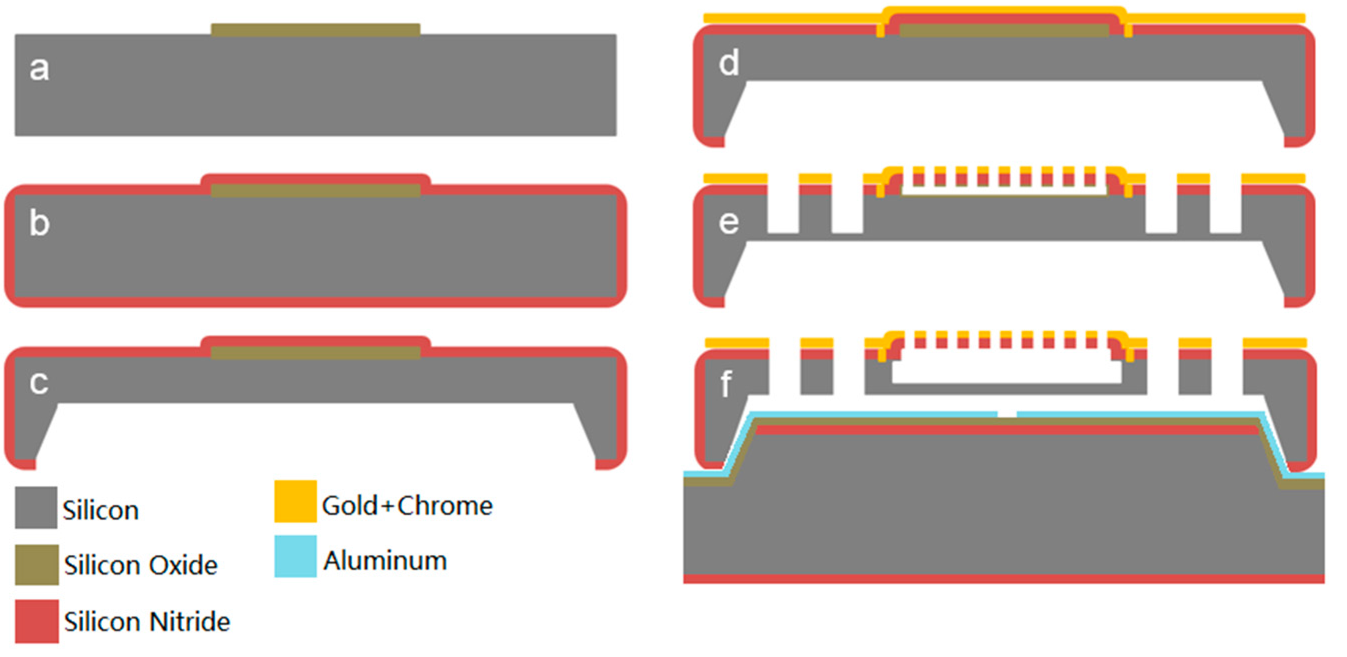
Figure 12.
(a) A SEM image of the MEMS scanning mirror with adjustable focus; (b) An optical microscopy image of the bottom quad-electrode pillar. Reproduced with permission from Lin, L.Y., Optics Express; published by OSA Publishing, 2013.
Figure 12.
(a) A SEM image of the MEMS scanning mirror with adjustable focus; (b) An optical microscopy image of the bottom quad-electrode pillar. Reproduced with permission from Lin, L.Y., Optics Express; published by OSA Publishing, 2013.
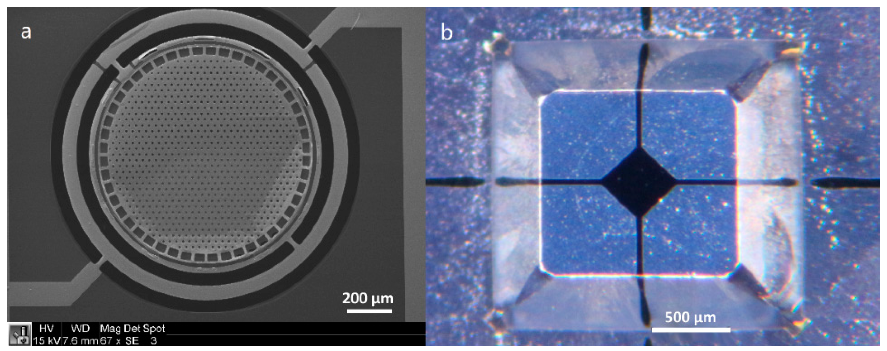
Figure 13.
Experimental results for the radius-of-curvature control generated by applying a voltage between the mirror membrane and the Si frame underneath. Three corresponding optical surface profiler images at 50, 80 and 95 V applied bias are also shown. Reproduced with permission from Lin, L.Y., Optics Express; published by OSA Publishing, 2013.
2.3. Electromagnetic Actuation
Electromagnetic actuation has also been explored to achieve MEMS scanning mirrors for biomedical imaging [11,15]. In reference [11], copper driving coils were electro-plated on the scanning mirror, which together with external permanent magnets formed the actuation structure. The mirror was 4.2 mm × 3.0 mm in size; it had resonant frequencies around 4 kHz; and it achieved a mechanical scanning range up to 8°. This scanning micromirror was used in a commercial Olympus confocal laser scanning microscope. In reference [15], a MEMS scanning catheter was developed for 3D endoscopic imaging with spectral-domain OCT. The two-axis scanning micromirror was fabricated on a SOI wafer, and after the fabrication was completed, a thin magnetic layer composed of a small NdFeB magnet was glued to the back of the micromirror manually. The packaged catheter had an outer diameter of 2.8 mm, and the resonant frequencies of the micromirror were 450 and 350 Hz for the inner and outer axes, respectively. It achieved a mechanical scanning range of ±10°. Since electromagnetic actuation mainly draws current, the actuation voltage was low (1–3 V). In vivo 3D images of human fingertips and oral cavity tissue were obtained to demonstrate the functionality of the scanning micromirror.
2.4. Piezoelectric Actuation
More recent explorations have incorporated the piezoelectric effect to actuate scanning mirrors due to its ability to achieve large static deflection with low power consumption while still boasting high speed. Owing to its ability to achieve both high resonant frequencies and significant static displacement, piezoelectric actuation supports flexibility in scan speed and imaging.
In particular, lead zirconate titanate (PZT) has emerged as a highly piezoelectric material exhibiting large actuation forces as compared to other piezoelectric films, and PZT is readily micromachinable in MEMS applications [44]. In reference [45], the authors demonstrated the utility of PZT piezoelectric transduction in a dual-mirror system oriented in a forward-looking probe, which is especially advantageous in evaluating larger or hollow organs. In this particular system, the mirror attaches at the end of a multilayer cantilever employing PZT as the actuation mechanism. The device developed from a thermally oxidized wafer followed by steps to create the piezoelectric actuator and the scanning mirror; in a two-step etch and release process, the authors independently defined the thickness of the optical mirror and that of the cantilever arm. Contrary to a tradeoff in previous fabrication methods, this procedure resulted in good control of both the actuation range and mirror smoothness, yielding mirror sizes of 600 μm × 840 μm and 700 μm × 1300 μm. The 600 μm × 840 μm mirrors produced a near-static scan range of ±7° at an actuation voltage of 20 V peak-to-peak with a maximum measured power consumption of 1 mW, and under resonant actuation and a voltage amplitude of 1.8 V, the mirror achieved an approximately ±8° response. With a 400 μm cantilever length, the two mirrors possessed resonant frequencies of 600 and 200 Hz, respectively. By reducing the cantilever to 200 μm, the resonant frequencies increased to as much as 2 kHz; however, a shorter cantilever results in reduced deflection. The micromirror was successfully demonstrated in a Fourier domain-OCT system.
Reducing the thickness of the PZT layer can result in larger displacements. An example was reported in reference [46], where a thin-film piezoelectric microactuator comprised of PZT was implemented and purposed for obtaining both lateral and vertical cross-sectioning in endoscopic dual-axes confocal imaging. In the MEMS architecture employing an SOI process flow, a dog-bone shaped mirror is connected to a gimbal platform by beam flexures, and the gimbal base is supported by outer folded legs with embedded thin-film PZT. The outer legs provide the mirror vertical translation, given the large range of motion induced by the thin-films. To actuate the inner mirror, high-frequency excitation of the PZT coupled resonant motion into the mirror for rotational scanning. With this scheme, the authors achieved nearly 200 μm of vertical translation at 18 V with a rotational motion of ±5.5° under 2 V AC actuation. Power requirements under resonance were on the order of 30 μW. The resonant frequency was observed as 3.8 kHz when holes were etched in the mirror platform, and 2.8 kHz for a solid mirror coated with gold. The system provided a field of view of 800 μm × 200 μm and was sized appropriately for application in endoscopy.
3. Image Correction
Image distortions can be caused by various mechanisms during image acquisition utilizing scanning mirrors. For example, the radial scan from the MEMS mirror can cause various distortions in OCT images, since an OCT interferogram is encoded with optical path length difference, potentially causing flat surfaces to appear curved. Conventionally, this type of distortion was corrected using algorithms based on a point-to-point method [47,48], which can consume substantial computing resources. In reference [49], the authors discuss a new method that directly manipulates the original spectral interferograms in the phase domain to correct the spherical distortion. The algorithm continues with a Fourier transform and 3D geometrical transformation to correct fan-shaped and keystone distortions.
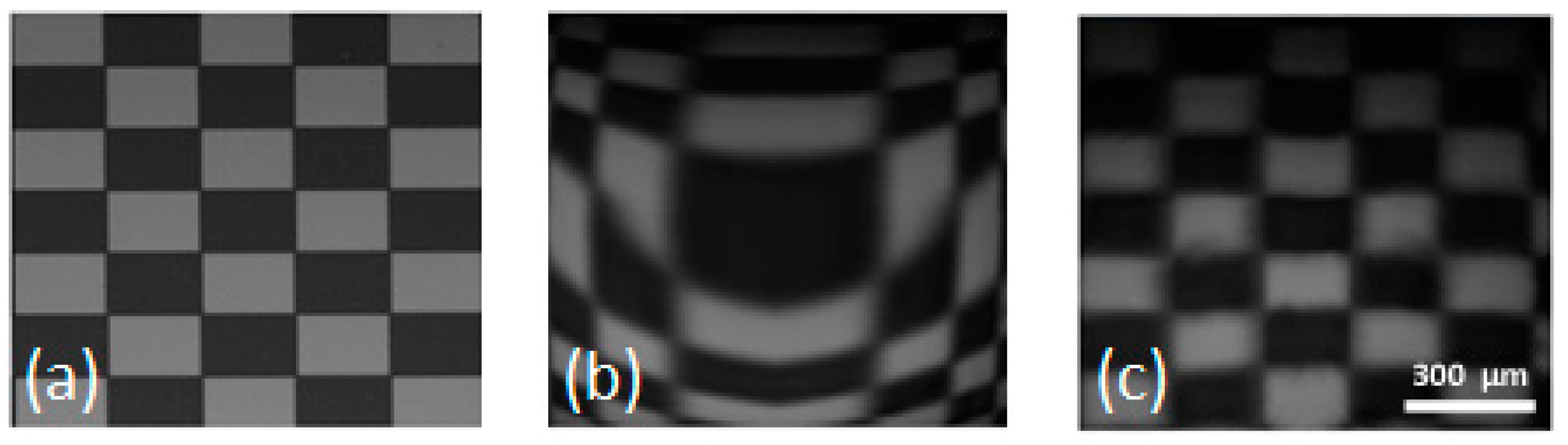
Due to the non-linear nature of the gap-closing electrostatic actuation mechanism when driven at non-resonant frequencies, calibration of the driving waveforms is necessary for linear spatial scanning in 2D transverse imaging. This can be achieved through mapping the spatial displacement of the optical beam for a given array of input voltages. Reference [18] shows an example of successful image correction through this approach. In addition to the above-mentioned distortion mechanisms, resonant scanning in one direction demands higher frequencies, which introduce further distortion and divergence from theory. In reference [18], a local transformation-based method was further introduced to correct all distortion mechanisms in the calibration process. There are four key steps in this approach: (1) establish feature-point correspondences between the distorted image and the ground-truth image; (2) parameterize the distorted image and the ground-truth image, respectively, with the feature points; (3) compute the local warping parameters from the corresponding sub-region around each feature point; (4) de-warp the distorted image by applying the local warping parameters. Figure 14 demonstrates the result of the local de-warping image correction algorithm. The as-acquired image (Figure 14b) is substantially distorted from the ground-truth image taken under an optical microscope (Figure 14a). After applying the algorithm, the image is corrected (Figure 14c) and becomes much closer to the original target image.
Reference [18] further discussed using a scanning speed correction technique [50] to correct the distorted image obtained through a spectral-domain OCT system due to non-linear spatial movement of the MEMS scanning mirror. The technique utilizes the cross-correlation between adjacent A-scans to estimate their lateral displacement. This relation enables interpolation to uniformly re-distribute A-scans along the lateral axis. The processing time for one frame of 1000 A-scans required approximately 0.2 s when implemented in MATLAB® (Natick, MA, USA). With a further optimized processing scheme, reference [50] achieved a rate of over 62,000 A-scans per second using a graphical processing unit (GPU) and parallel processing, thereby demonstrating the compatibility of this algorithm with real-time imaging. In reference [18], a mouse ear was imaged using spectral-domain OCT with a 2D MEMS scanning mirror. The corrected image after applying the scan-speed correction technique demonstrated elimination of motion artifacts.
Figure 14.
Results of imaging correction using a local de-warping algorithm. (a) Optical microscope image of the target; (b) Image acquired through an electrostatic-actuated two-axis MEMS scanning mirror without any calibration and correction; (c) Corrected image after applying the local de-warping algorithm. Reproduced with permission from Lin, L.Y., Biomedical Optics Express; published by OSA Publishing, 2015.
4. Summary
In this paper, we review the progress of MEMS scanning mirrors for optical bio-imaging applications. We discuss the principles of various actuation mechanisms and summarize the performance of scanning micromirrors achieved by each actuation technology. In general, thermoelectric actuation can achieve large scanning angles for the micromirrors, and the overall device area can be compact; however, the actuation draws large currents, and the speed may be reduced due to thermal relaxation time. Electromagnetic actuation can in principle achieve large scanning angles, but it requires magnetic materials which can make fabrication and packaging of compact devices more challenging. Like thermoelectric actuation, it requires low actuation voltage but has a similar issue with current draw. Electrostatic actuation typically requires high voltages but consumes very little power since it draws almost no current. Two main approaches have been developed for electrostatic actuation: comb-drive and parallel-plate gap-closing actuators. The former can achieve linear actuation but in general results in larger device areas, while the latter can achieve compact device areas but the actuation is non-linear if not operated at resonance. More recent investigations have shown that piezoelectric actuation is another viable mechanism that can achieve large deflections in both the resonant and static cases, while also requiring less power; however, design and fabrication of these structures can be complex requiring materials not necessarily native to CMOS processing.
We also discuss additional functionality such as tunable focal lengths that can enhance MEMS scanning mirrors, and we show realization of the integrated devices using both electrothermal and electrostatic actuation approaches. The scanning motion of the MEMS mirrors can result in various artifacts during image acquisition, and various algorithms have been developed to correct distortions to improve image quality. Some of the demonstrated results are summarized in this paper.
MEMS scanning mirror technologies have made substantial impacts in many applications, with optical imaging in biomedicine being a significant one of them. Given the continuous efforts in this field, it is expected that the performance of these MEMS scanning mirrors will continue to improve which will enable optical imaging with higher resolution, speed, and functionality in more compact devices and systems.
Acknowledgments
We thank Ming-Ting Sun and Ruikang Wang (University of Washington), Xingde Li (Johns Hopkins University), and Mingli Song (Zhejiang University) for helpful discussions that resulted in part of the work described in this paper. Part of the work was supported by National Institutes of Health (Grant # R01 EB007636). Ethan Keeler is supported by the National Science Foundation Graduate Research Fellowship Program under Grant No. DGE-1256082.
Author Contributions
Both L.Y.L. and E.G.K. contributed to the writing of this paper. E.G.K. contributed to part of the experiments described in this review.
Conflicts of Interest
The authors declare no conflict of interest.
References
- Pawley, J.B. Handbook of Biological Confocal Microscopy; Plenum Press: New York, NY, USA, 1995. [Google Scholar]
- Huang, D.; Swanson, E.A.; Lin, C.P.; Schuman, J.S.; Stinson, W.G.; Chang, W.; Hee, M.R.; Flotte, T.; Gregory, K.; Puliafito, C.A.; et al. Optical coherence tomography. Science 1991, 254, 1178–1181. [Google Scholar] [CrossRef] [PubMed]
- Denk, W.; Strickler, J.H.; Webb, W.W. Two-photon laser scanning fluorescence microscopy. Science 1990, 248, 73–76. [Google Scholar] [CrossRef] [PubMed]
- Zipfel, W.R.; Williams, R.M.; Webb, W.W. Nonlinear magic: Multiphoton microscopy in the biosciences. Nat. Biotechnol. 2003, 21, 1369–1377. [Google Scholar] [CrossRef] [PubMed]
- Tearney, G.J.; Brezinski, M.E.; Bouma, B.E.; Boppart, S.A.; Pitris, C.; Southern, J.F.; Fujimoto, J.G. In vivo endoscopic optical biopsy with optical coherence tomography. Science 1997, 276, 2037–2039. [Google Scholar] [CrossRef] [PubMed]
- Tearney, G.J.; Brezinski, M.E.; Fujimoto, J.G.; Weissman, N.J.; Boppart, S.A.; Bouma, B.E.; Southern, J.F. Scanning single-mode fiber optic catheter–endoscope for optical coherence tomography. Opt. Lett. 1996, 21, 543–545. [Google Scholar] [CrossRef] [PubMed]
- Liu, X.; Cobb, M.J.; Chen, Y.; Kimmey, M.B.; Li, X. Rapid-scanning forward-imaging miniature endoscope for real-time optical coherence tomography. Opt. Lett. 2004, 29, 1763–1765. [Google Scholar] [CrossRef] [PubMed]
- Seibel, E.J.; Smithwick, Q.Y.J. Unique features of optical scanning, single fiber endoscopy. Lasers Surg. Med. 2002, 30, 177–183. [Google Scholar] [CrossRef] [PubMed]
- Arrasmith, C.L.; Dickensheets, D.L.; Mahadevan-Jansen, A. Mems-based handheld confocal microscope for in vivo skin imaging. Opt. Express 2010, 18, 3805–3819. [Google Scholar] [CrossRef] [PubMed]
- Dickensheets, D.L.; Kino, G.S. Silicon-micromachined scanning confocal optical microscope. J. Microelectromech. Syst. 1998, 7, 38–47. [Google Scholar] [CrossRef]
- Miyajima, H.; Asaoka, N.; Isokawa, T.; Ogata, M.; Aoki, Y.; Imai, M.; Fujimori, O.; Katashiro, M.; Matsumoto, K. A mems electromagnetic optical scanner for a commercial confocal laser scanning microscope. J. Microelectromech. Syst. 2003, 12, 243–251. [Google Scholar] [CrossRef]
- Piyawattanametha, W.; Hyejun, R.; Mandella, M.J.; Loewke, K.; Wang, T.D.; Kino, G.S.; Solgaard, O.; Contag, C.H. 3D near-infrared fluorescence imaging using an mems-based miniature dual-axis confocal microscope. IEEE J. Sel. Top. Quantum Electron. 2009, 15, 1344–1350. [Google Scholar] [CrossRef]
- Piyawattanametha, W.; Ra, H.; Qiu, Z.; Friedland, S.; Liu, J.T.C.; Loewke, K.; Kino, G.S.; Solgaard, O.; Wang, T.D.; Mandella, M.J.; et al. In vivo near-infrared dual-axis confocal microendoscopy in the human lower gastrointestinal tract. J. Biomed. Opt. 2012, 17, 0211021–0211024. [Google Scholar] [CrossRef] [PubMed]
- Liu, L.; Wang, E.; Zhang, X.; Liang, W.; Li, X.; Xie, H. Mems-based 3D confocal scanning microendoscope using memsscanners for both lateral and axial scan. Sens. Actuators A 2014, 215, 89–95. [Google Scholar] [CrossRef] [PubMed]
- Kim, K.H.; Park, B.H.; Maguluri, G.N.; Lee, T.W.; Rogomentich, F.J.; Bancu, M.G.; Bouma, B.E.; de Boer, J.F.; Bernstein, J.J. Two-axis magnetically-driven mems scanning catheter for endoscopic high-speed optical coherence tomography. Opt. Express 2007, 15, 18130–18140. [Google Scholar] [CrossRef] [PubMed]
- Jung, W.; Zhang, J.; Wang, L.; Wilder-Smith, P.; Chen, Z.; McCormick, D.T.; Tien, N.C. Three-dimensional optical coherence tomography employing a 2-axis microelectromechanical scanning mirror. IEEE J. Sel. Top. Quantum Electron. 2005, 11, 806–810. [Google Scholar] [CrossRef]
- Yang, V.X.D.; Mao, Y.; Standish, B.A.; Munce, N.R.; Chiu, S.; Burnes, D.; Wilson, B.C.; Vitkin, I.A.; Himmer, P.A.; Dickensheets, D.L. Doppler optical coherence tomography with a micro-electro-mechanical membrane mirror for high-speed dynamic focus tracking. Opt. Lett. 2006, 31, 1262–1264. [Google Scholar] [CrossRef] [PubMed]
- Strathman, M.; Liu, Y.; Keeler, E.G.; Song, M.; Baran, U.; Xi, J.; Sun, M.-T.; Wang, R.; Li, X.; Lin, L.Y. Mems scanning micromirror for optical coherence tomography. Biomed. Opt. Express 2015, 6, 211–224. [Google Scholar] [CrossRef] [PubMed]
- Aguirre, A.D.; Hertz, P.R.; Chen, Y.; Fujimoto, J.G.; Piyawattanametha, W.; Fan, L.; Wu, M.C. Two-axis mems scanning catheter for ultrahigh resolution three-dimensional and en face imaging. Opt. Express 2007, 15, 2445–2453. [Google Scholar] [CrossRef] [PubMed]
- Jain, A.; Kopa, A.; Pan, Y.; Fedder, G.K.; Xie, H. A two-axis electrothermal micromirror for endoscopic optical coherence tomography. IEEE J. Sel. Top. Quantum Electron. 2004, 10, 636–642. [Google Scholar] [CrossRef]
- Sun, J.; Guo, S.; Wu, L.; Liu, L.; Choe, S.-W.; Sorg, B.S.; Xie, H. 3D in vivo optical coherence tomography based on a low-voltage, large-scan-range 2D mems mirror. Opt. Express 2010, 18, 12065–12075. [Google Scholar] [CrossRef] [PubMed]
- Piyawattanametha, W.; Barretto, R.P.J.; Ko, T.H.; Flusberg, B.A.; Cocker, E.D.; Ra, H.; Lee, D.; Solgaard, O.; Schnitzer, M.J. Fast-scanning two-photon fluorescence imaging based on a microelectromechanical systems two-dimensional scanning mirror. Opt. Lett. 2006, 31, 2018–2020. [Google Scholar] [CrossRef] [PubMed]
- Morrison, J.; Imboden, M.; Little, T.D.C.; Bishop, D.J. Electrothermally actuated tip-tilt-piston micromirror with integrated varifocal capability. Opt. Express 2015, 23, 9555–9566. [Google Scholar] [CrossRef] [PubMed]
- Dickensheets, D.L. Requirements of mems membrane mirrors for focus adjustment and aberration correction in endoscopic confocal and optical coherence tomography imaging instruments. J. Micro Nanolithogr. MEMS MOEMS 2008, 7, 021008. [Google Scholar] [CrossRef]
- Qi, B.; Himmer, P.A.; Gordon, M.L.; Yang, V.X.D.; Dickensheets, D.L.; Vitkin, I.A. Dynamic focus control in high-speed optical coherence tomography based on a microelectromechanical mirror. Opt. Commun. 2004, 232, 123–128. [Google Scholar] [CrossRef]
- Sasaki, T.; Hane, K. Initial deflection of silicon-on-insulator thin membrane micro-mirror and fabrication of varifocal mirror. Sens. Actuators A Phys. 2011, 172, 516–522. [Google Scholar] [CrossRef]
- Strathman, M.; Liu, Y.; Li, X.; Lin, L.Y. Dynamic focus-tracking mems scanning micromirror with low actuation voltages for endoscopic imaging. Opt. Express 2013, 21, 23934–23941. [Google Scholar] [CrossRef] [PubMed]
- Xie, H.; Pan, Y.; Fedder, G.K. Endoscopic optical coherence tomographic imaging with a cmos-mems micromirror. Sens. Actuators A 2003, 103, 237–241. [Google Scholar] [CrossRef]
- Fu, L.; Jain, A.; Xie, H.; Cranfield, C.; Gu, M. Nonlinear optical endoscopy based on a double-clad photonic crystal fiber and a mems mirror. Opt. Express 2006, 14, 1027–1032. [Google Scholar] [CrossRef] [PubMed]
- Samuelson, S.R.; Wu, L.; Sun, J.; Choe, S.-W.; Sorg, B.S.; Xie, H. A 2.8-mm imaging probe based on a high-fill-factor mems mirror and wire-bonding-free packaging for endoscopic optical coherence tomography. J. Microelectromechanical Syst. 2012, 21, 1291–1302. [Google Scholar] [CrossRef]
- Liu, W.; Talghader, J.J. Current-controlled curvature of coated micromirrors. Opt. Lett. 2003, 28, 932–934. [Google Scholar] [CrossRef] [PubMed]
- Singh, J.; Teo, J.H.S.; Xu, Y.; Premachandran, C.S.; Chen, N.; Kotlanka, R.; Olivo, M.; Sheppard, C.J.R. A two axes scanning soi mems micromirror for endoscopic bioimaging. J. Micromech. Microeng. 2008, 18, 025001. [Google Scholar] [CrossRef]
- Jung, W.; McCormick, D.T.; Zhang, J.; Wang, L.; Tien, N.C.; Chen, Z. Three-dimensional endoscopic optical coherence tomography by use of a two-axis microelectromechanical scanning mirror. Appl. Phys. Lett. 2006, 88, 163901. [Google Scholar] [CrossRef]
- Karthik, K.; Jonathan, C.C.; Austin, M.; Nate, J.K.; Kazunori, H.; Thomas, E.M.; Xiaojing, Z. Fast 3d in vivo swept-source optical coherence tomography using a two-axis mems scanning micromirror. J. Opt. A Pure Appl. Opt. 2008, 10, 044013. [Google Scholar] [CrossRef]
- Hyejun, R.; Piyawattanametha, W.; Taguchi, Y.; Lee, S.; Mandella, M.J.; Solgaard, O. Two-dimensional mems scanner for dual-axes confocal microscopy. J. Microelectromech. Syst. 2007, 16, 969–976. [Google Scholar] [CrossRef]
- Maitland, K.C.; Shin, H.J.; Ra, H.; Lee, D.; Solgaard, O.; Richards-Kortum, R. Single fiber confocal microscope with a two-axis gimbaled mems scanner for cellular imaging. Opt. Express 2006, 14, 8604–8612. [Google Scholar] [CrossRef] [PubMed]
- Liu, J.T.C.; Mandella, M.J.; Ra, H.; Wong, L.K.; Solgaard, O.; Kino, G.S.; Piyawattanametha, W.; Contag, C.H.; Wang, T.D. Miniature near-infrared dual-axes confocal microscope utilizing a two-dimensional microelectromechanical systems scanner. Opt. Lett. 2007, 32, 256–258. [Google Scholar] [CrossRef] [PubMed]
- Piyawattanametha, W.; Wang, T.D. Mems-based dual-axes confocal microendoscopy. IEEE J. Sel. Top. Quantum Electron. 2010, 16, 804–814. [Google Scholar] [CrossRef] [PubMed]
- Wang, T.D.; Mandella, M.J.; Contag, C.H.; Kino, G.S. Dual-axis confocal microscope for high-resolution in vivo imaging. Opt. Lett. 2003, 28, 414–416. [Google Scholar] [CrossRef] [PubMed]
- Jae-Woong, J.; Sunwoo, K.; Solgaard, O. Split-frame gimbaled two-dimensional mems scanner for miniature dual-axis confocal microendoscopes fabricated by front-side processing. J. Microelectromech. Syst. 2012, 21, 308–315. [Google Scholar] [CrossRef]
- Yeow, J.T.W.; Yang, V.X.D.; Chahwan, A.; Gordon, M.L.; Qi, B.; Vitkin, I.A.; Wilson, B.C.; Goldenberg, A.A. Micromachined 2D scanner for 3D optical coherence tomography. Sens. Actuators A Phys. 2005, 117, 331–340. [Google Scholar] [CrossRef]
- Hokari, R.; Hane, K. Micro-mirror laser scanner combined with a varifocal mirror. Microsyst. Technol. 2012, 18, 475–480. [Google Scholar] [CrossRef]
- Shao, Y.; Dickensheets, D.L. Moems 3D scan mirror for single-point control of beam deflection and focus. MOEMS 2005, 4, 041502. [Google Scholar] [CrossRef]
- Beeby, S.P.; Blackburn, A.; White, N.M. Processing of PZT piezoelectric thick films on silicon for microelectromechanical systems. J. Micromech. Microeng. 1999, 9, 218–229. [Google Scholar] [CrossRef]
- Gilchrist, K.H.; McNabb, R.P.; Izatt, J.A.; Grego, S. Piezoelectric scanning mirrors for endoscopic optical coherence tomography. J. Micromech. Microeng. 2009, 19, 095012. [Google Scholar] [CrossRef]
- Qiu, Z.; Rhee, C.-H.; Choi, J.; Wang, T.D.; Oldham, K.R. Large stroke verticle pzt microactuator with high-speed rotational scanning. J. Microelectromech. Syst. 2014, 23, 256–258. [Google Scholar] [CrossRef] [PubMed]
- Ortiz, S.; Siedlecki, D.; Remon, L.; Marcos, S. Optical coherence tomography for quantitative surface topography. Appl. Opt. 2009, 48, 6708–6715. [Google Scholar] [CrossRef] [PubMed]
- Podoleanu, A.; Charalambous, I.; Plesea, L.; Dogariu, A.; Rosen, R. Correction of distortions in optical coherence tomography imaging of the eye. Phys. Med. Biol. 2004, 49, 1277. [Google Scholar] [CrossRef] [PubMed]
- Wang, D.; Liang, P.; Samuelson, S.; Jia, H.; Ma, J.; Xie, H. Correction of image distortions in endoscopic optical coherence tomography based on two-axis scanning mems mirrors. Biomed. Opt. Express 2013, 4, 2066–2077. [Google Scholar] [CrossRef] [PubMed]
- Liu, X.; Huang, Y.; Kang, J.U. Distortion-free freehand-scanning OCT implemented with real-time scanning speed variance correction. Opt. Express 2012, 20, 16567–16583. [Google Scholar] [CrossRef]
© 2015 by the authors; licensee MDPI, Basel, Switzerland. This article is an open access article distributed under the terms and conditions of the Creative Commons by Attribution (CC-BY) license (http://creativecommons.org/licenses/by/4.0/).
Share and Cite
MDPI and ACS Style
Lin, L.Y.; Keeler, E.G. Progress of MEMS Scanning Micromirrors for Optical Bio-Imaging. Micromachines 2015, 6, 1675-1689. https://doi.org/10.3390/mi6111450
AMA Style
Lin LY, Keeler EG. Progress of MEMS Scanning Micromirrors for Optical Bio-Imaging. Micromachines. 2015; 6(11):1675-1689. https://doi.org/10.3390/mi6111450
Chicago/Turabian StyleLin, Lih Y., and Ethan G. Keeler. 2015. "Progress of MEMS Scanning Micromirrors for Optical Bio-Imaging" Micromachines 6, no. 11: 1675-1689. https://doi.org/10.3390/mi6111450