Abstract
A series of technological steps concentrating around photolithography and UV polymer on glass replication in a mask-aligner that allow for the cost-effective generation of rather complex micro-optical systems on the wafer level are discussed. In this approach, optical functional surfaces are aligned to each other and stacked on top of each other at a desired axial distance. They can consist of lenses, achromatic doublets, regular or chirped lens arrays, diffractive elements, apertures, filter structures, reflecting layers, polarizers, etc. The suitability of the separated modules in certain imaging and non-imaging applications will be shown.
1. Introduction
Although discussed extensively in recent years, wafer level optics is a well-established technology, which had been introduced decades ago in the field of miniaturized or micro-structured optics. Here, the wafer concept was simply related to the lithographical generation of micro-optical structures, such as microlens arrays or diffractive optical elements. In analogy to micro-electronics, a large number of optical chips with thousands or millions of microstructures can be generated in parallel. Lithography involves the structuring of several layers, aligned to each other, and, thus, offers an integration capability. More than ten years ago, UV polymer on glass replication [1] using a modified mask aligner as a lithography related fabrication tool was introduced as a precise and cost effective technology for the generation of wafer-scale miniaturized optical systems and for hybrid integration [2]. Parallel fabrication is especially useful in cases of miniaturized systems because one can obtain a high number of chips from a wafer and in cases where several structural layers have to be aligned to each other. Thus, similar wafer-level concepts were introduced and optimized in recent years for the fabrication of miniaturized cameras [3,4,5]. However, the technological and application potential of wafer-level miniaturized optics is not restricted to miniature camera lenses.
In the present paper we present a refined wafer-level fabrication technology involving UV polymer molding, coating and lithography which is based on earlier work [2] but is characterized by a much higher degree of variety and complexity. Within the frame of this paper, the main focus will be on the diversity of systems that have been realized using this technology, as well as on the fabrication details, range of parameters, and on the potential and limits of the approach. The paper is organized as follows: the mastering of micro-optical elements, UV replication, and further key elements of the fabrication process will be discussed in the next chapter “Technology”. Our focus is on the interaction and compatibility of process steps in order to generate systems with high lateral and axial complexity. This will be illustrated in the subsequent chapter “Experimental examples and characterization” by discussing special aspects of three different micro-optical systems. Finally, a summary of typical systems, their performance and main technological parameters will be given and conclusions will be drawn.
2. Technology
2.1. UV Polymer Molding
The centerpiece of the presented technology is a UV polymer molding process using a mask aligner. In the typical UV replication, a thin layer of polymer is cured in between a replication tool and a rigid inorganic substrate such as glass. In fact, the low coefficient of thermal expansion (CTE), good optical homogeneity and low total thickness variation of state-of-the-art float glass wafers, such as Borofloat B33 or D263T (Schott), are essential in order to realize the necessary lateral and axial precision of micro-optical systems on a wafer level. UV polymer (cured at room temperature and normal pressure) is used to realize high precision, rapid replication, and good adhesion to the substrate and high thermal and environmental stability of the element. There are numerous acrylate- or epoxy-based UV curing resins with tailored properties, such as viscosity, refractive index, or shrinkage, which are compatible with the described UV-molding process. Inorganic-organic hybrid polymers like ORMOCOMP® [6,7] show enhanced stability compared to their purely organic counterparts.
A contact mask aligner is ideally suited to generate thin, uniform and plane-replicated polymer layers on arbitrary substrates as a result of a sequence of dispensing, alignment, proximity exposure through a UV-transparent mold, and separation. In our experiments we used a MA8e 200 mm aligner (SUSS MicroTec AG, Munich, Germany) featuring a unique UV molding software and a special tooling with exposure gap control realized by three-point inductive z-measurement and closed-loop piezo-driven z-axis movement for sub- µm gap control. Furthermore the piezo-driven z-movement is designed to apply the necessary force to spread the dispensed polymer resin across a 200 mm wafer area.
For proper focusing of the individual systems on the wafer a high axial precision is essential. This is achieved by the precise mask aligner tooling, especially the top load mask holder approach and due to soft elastomer-on-glass molds, which were fabricated using the same mask aligner, thus, compensating for some of the deviations. In the MA8e, the substrate thickness can be as high as 10 mm, and the mask or replication tool can be as thick as 15 mm in order to ensure superior planarity. Alternatively, thinner replication tools can be reinforced by a vacuum-attached, planar, transparent glass plate. As a result, it is possible to replicate UV cured, insoluble polymer films on either side of arbitrary substrates, even on top of each other with a lateral precision of about ±1 µm across 200 mm substrates and an axial accuracy in the range of ±5 µm. Typically the overall polymer thickness exceeds the lens sag, forming a uniform polymer layer in order to accomplish axial alignment and as a means for shrinkage compensation. For a lens sag <150 µm, we found that for a polymerization shrinkage below 5% (volume) it is not necessary to apply some form of mold precompensation in order to maintain the diffraction limited lens accuracy during the molding step.
In the UV molding technology, the adhesion to the mold is kept low by a proper choice of the mold material (i.e., polydimethyl siloxane/PDMS) or by applying an anti-sticking layer onto the mold surface. Thus, the mold can be separated from the molded part after UV curing. On the other hand, when treated with an adhesion promoter, two parts can be aligned and glued together using the same process (without the separation). That means the technology is not restricted to single- or double-side polymer on glass replication but can be extended to stacks of wafers. An example concerning multi-aperture cameras is given in Chapter 3.3.
2.2. Coating and Structuring
Apertures filter structures, anti-reflection, or other coatings are an essential part in the design of more complex optical systems and have to be implemented in the wafer-level approach. The UV polymer on glass technology allows for a variety of different materials and arrangements of structural layers: a glass wafer can be coated and patterned before the replication, i.e., by sputter coating of metal, lithography, and wet etching. In this way, apertures or reflector elements were generated in chromium, low reflective chromium, titanium, aluminum and silver.
Additionally, the glass wafer can be structured using photopatternable polymer materials (like PSK2000 and PSC resists/Brewer science). Thus, apertures or color filters can be generated by spin coating, lithography, and hard bake. The choice of metal or polymer apertures depends on the actual design. PSK2000 apertures have very low reflection (<1%) in a wide spectral and angular range and are easily generated, while low reflective chromium structures demonstrate better spatial resolution and stability. Lens replication on top of apertures or filters results in buried structures.
Plane, transparent polymer layers can be added by UV-molding, defining additional structural layers or acting as spacers.
Surfaces can be coated with large-area dielectric layer systems, i.e., as IR cutoff or other filters anti-reflection coatings or mirrors. Plasma assisted evaporation (APS) coating technology for polymer surfaces is a well-established technology [8] and can be applied to optical wafers in every stage of the fabrication. Typically, UV polymer is subject to a thermal post-curing (hardbake) before coating (30 min at 180 °C under protective gas (Nitrogen) for ORMOCOMP®). We found that long-term radius changes of the ORMOCOMP® polymer lenses after hard bake were well below 1%.
2.3. Compatibility
As a matter of course, blank glass substrates can be structured in various ways. UV polymer replication is compatible with blank glass substrates, as well as with structured ones. Surface profiles will be planarized in the molding step and absorbing layers, apertures etc. are uncomplicated when using a UV-transparent replication tool. The crosslinked nature of UV-cured resins enables UV molding of several polymer layers directly on top of each other. Adhesion at interfaces is promoted by common silane treatment of glass or other oxidic surfaces [9], by proper choice of polymer materials, and by oxygen plasma treatment of polymer surfaces [8,10]. Dielectric coatings can be treated with silane adhesion promoters in the same way as glass as the final layer is usually SiO2. In this way, black matrix polymer apertures can for instance be created directly on top of anti-reflection coated lenses. The alternate stacking of UV-replicated polymer layers in the form of computer generated holograms and of dielectric color filter layers has already been demonstrated [11]. Shrinkage and CTE mismatch might cause problems like stress, wafer bowing, or delamination in the described stacks of different materials. This can limit the maximum polymer thickness especially in the case of thin glass substrates. As an alternative, a large area polymer layer can be subdivided into a multitude of smaller areas by proper tooling, by selective UV curing, or by a chipwise dispensing approach. Furthermore, symmetrical polymer-glass-polymer designs and/or flexible polymer resins can reduce bowing.
The chemical stability of crosslinked UV-cured polymer films enables subsequent coating and lithographic patterning, i.e., the generation of metal structures/apertures by sputtering of titanium, spin-coating, baking, and structuring of photoresist, wet chemical etching, and resist stripping on top of a replicated optical surface [12].
The compatibility of the dimensional scaling of different structural layers is achieved by the consistent use of photolithography. A set of photomasks normally consists of a mask for the lens mastering (see below), the apertures, the filter structures and the spacers, including the respective features for alignment, process monitoring, dicing, etc. The lithographical patterning of all features, the tooling and UV molding including the alignment of all layers is done in the same mask aligner under comparable conditions.
As a preliminary conclusion it can be stated that the compatibility of UV polymer on glass replication, coating and lithography is the key factor for the variety of different systems that can be generated as it will be shown below. Figure 1 shows a schematic flow chart of the wafer-level fabrication of micro-optical systems using the described process steps.
2.4. Thermal Behavior
Refractive index as well as geometry changes with temperature, have to be considered in the optical design of imaging systems; for lens array applications a temperature dependent pitch can be critical. Thermo-optical coefficients of a 100 µm thick polymer layer on a B33 glass substrate were measured and are typically on the order of −0.0002 K−1. Geometry changes were determined by measuring polymer-on-glass microlens arrays in a mechanical profiler (Taylor Hobson Form Talysurf) at different temperatures, thus, taking the polymer on glass configuration into account. In Figure 2 changes of pitch and radius of curvature of a polymer (ORMOCOMP®) on glass (Borofloat 33/Schott) microlens array are plotted, as far as we know for the first time. Due to the scatter in the lenslet parameters it is crucial to compare corresponding lenslets, and to scan across a higher number of lenslets in order to improve the measurement contrast. The measured pitch variation corresponds to the CTE of the glass substrate (+3.3 × 10⁻⁶ K−1) and is almost two orders of magnitude smaller than for thermoplastic polymers. As a consequence of the restricted lateral expansion there is a slight decrease of the lens radius with temperature (1/R × dR/dT of 0.00016 K−1), thus, the radius change can partially compensate for the thermo-optical changes of focal length. We could not detect a temperature change of the <30 nm rms. form deviation of the lenslets.
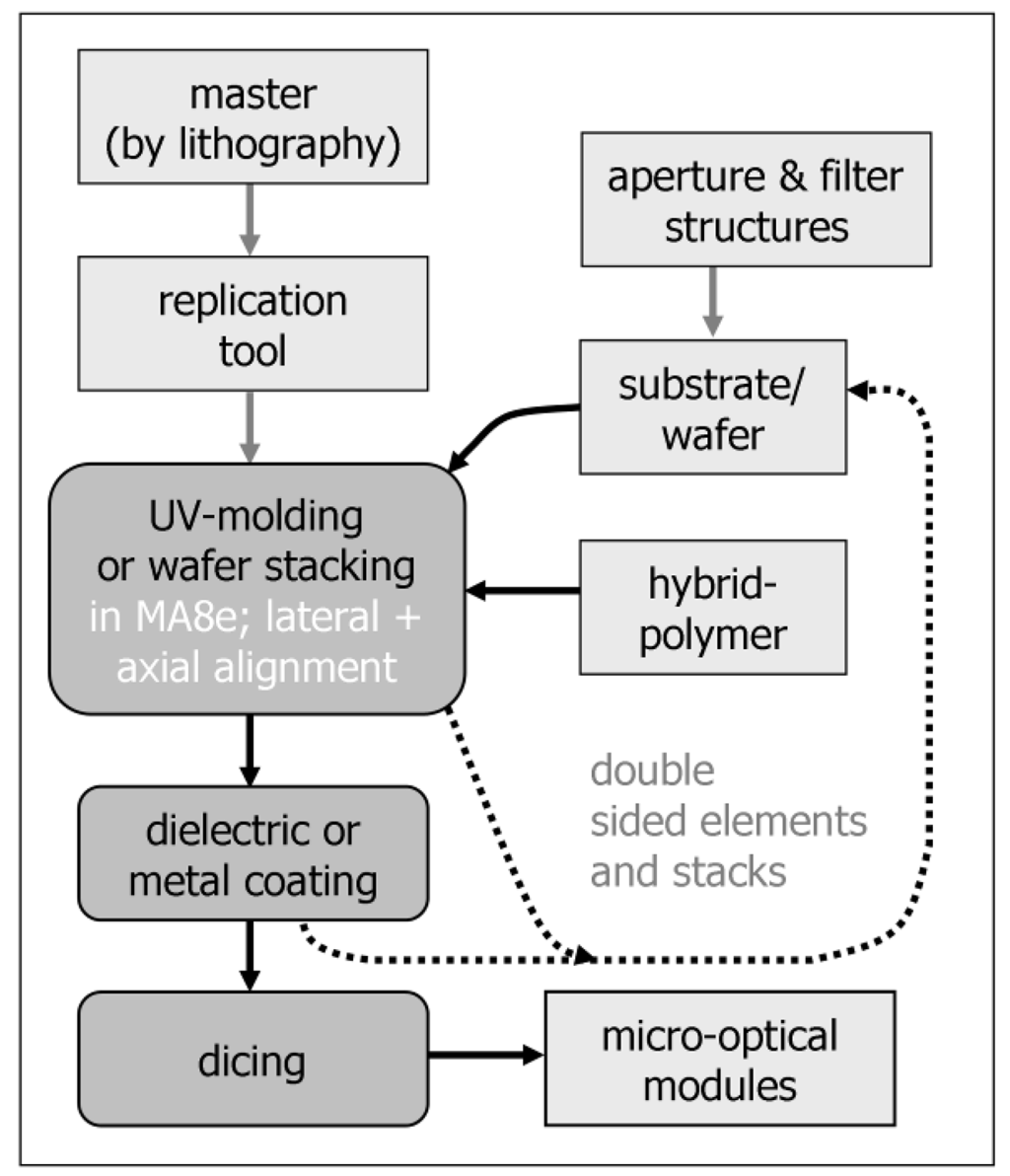
Figure 1.
Flowchart of the technology based on UV-molding, coating, and lithography.
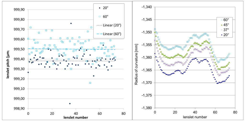
Figure 2.
Temperature dependent pitch (left hand side) and radius (Right hand side) changes of an ORMOCOMP® on B33 glass lens array measured using a mechanical profiler (FormTalysurf PGI/ Taylor Hobson).
2.5. Mastering by Photolithography
The reflow of photoresist patterned by binary photolithography is well established to generate a large number of microlens structures with precise positioning and diffraction limited surface accuracy on a single wafer [13,14,15]. The main limitations of the technology are the radius scatter depending on the amount of photoresist which is available per lenslet in the reflow step, and the limited flexibility of the lens profiles, both making reflow lenses less attractive for high-resolution imaging.
Nevertheless, in all of the applications discussed below we used reflow lens mastering successfully. Several extensions of the standard process enabling higher complexity of the systems will be discussed in the following paragraphs: hybrid refractive-diffractive elements, chirped lens arrays, and RIE assisted mastering.
Hybrid refractive-diffractive elements: here, the reflow process forming the refractive lens is carried out at reduced temperature so that the resist can still be patterned by further lithographical steps afterwards. In the example shown in Figure 3, we used variable dose laser writing to generate the diffractive correction element on top of the refractive microlens [16].
Chirped lens arrays: Figure 4 shows the scheme of a two-mask process where the lateral layout of the lens array is defined using mask #1. The structures are transferred to a ~100 nm thin base layer by dry etching, forming chemically stable lens pedestals. Then the proper resist thickness for the reflow process is added by spin coating. The volume of each lenslet (and thus its radius of curvature) is now defined by patterning a smaller resist area onto every pedestal using mask #2. As a result, the lateral lens layout (process #1) can be defined with exceptional high accuracy and high resolution, and can be chosen independently of the corresponding radius of curvature. In other words: every lenslet on the wafer can be designed to have its own position, orientation, size (mask #1), and focal length (mask #2). We used this enhanced design freedom in the randomization of arrays for homogenization [17], the channel-wise aberration correction of multichannel imaging optics [18] or simply the lateral arrangement of elements with different parameters on the same wafer [19]. A means to simulate “generalized” chirped or stochastic lens arrays in the ray tracing design and routines to calculate the corresponding mask data for each lenslet were implemented in our fabrication process [20].
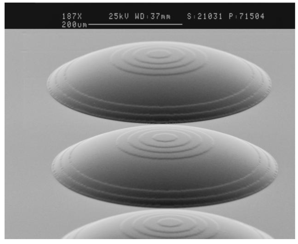
Figure 3.
Mastering of hybrid microlenses: refractive lens combined with a diffractive phase correction element by combining reflow and laser lithography.
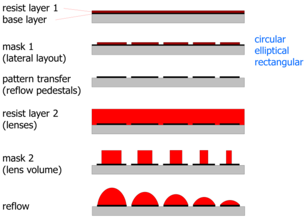
Figure 4.
Scheme of a two-mask process to generate chirped lens arrays.
RIE assisted lens mastering: Reactive ion etching (RIE) of polymer structures like reflow lenses is a well established technology for proportional transfer of lenses to fused silica or other inorganic substrates [21]. Furthermore, an initially spherical lens profile can be shaped by changing the transfer rate during the etch process resulting in well-defined aspheres [22]. The fabricated aspheres can be used as a master for UV replication [12]. The preferred substrate material in the RIE process is fused silica due to its etching characteristics, low CTE and UV transparency.
Because of the highly isotropic nature of the RIE, the fill factor of arrays of convex lenses decreases during the transfer process. On the other hand, with concave lens arrays it is constantly enhanced during the etching process until the gap between adjacent lenslets vanishes, leading to a 100% fill factor. Thus, a limitation of microlenses based on photoresist reflow can be overcome as shown in Figure 5. These arrays can again be used as a tool for subsequent UV replication.
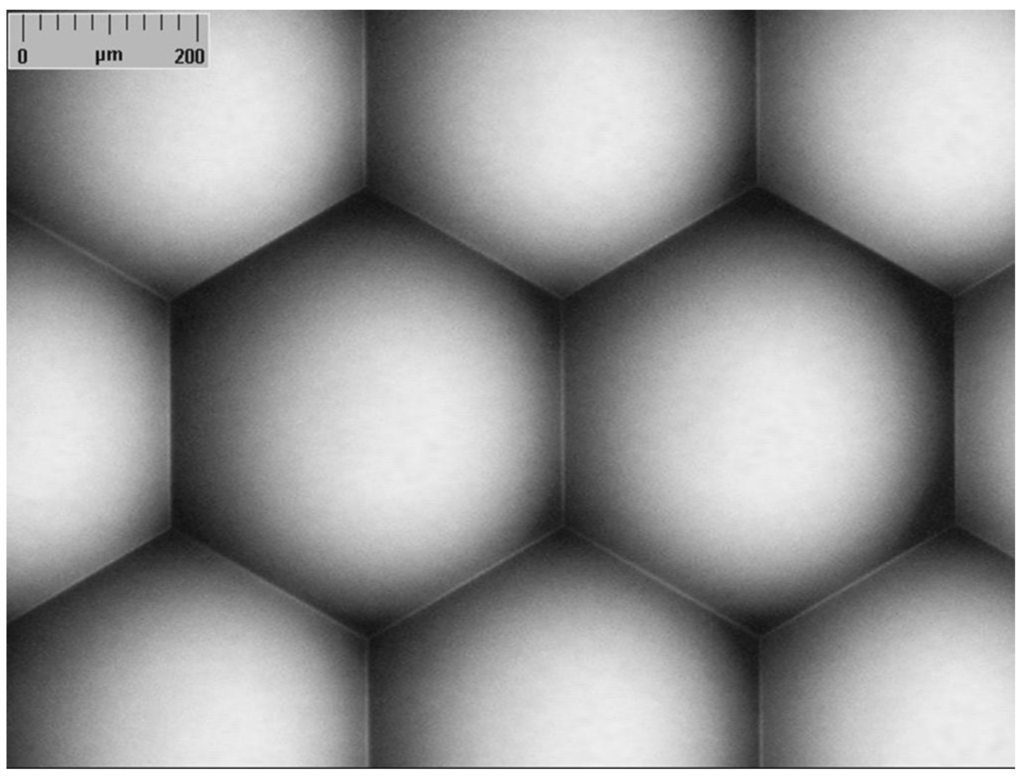
Figure 5.
Microscope photograph of a UV molded hexagonal convex lens array with 100% fill factor.
RIE assisted mastering is subject to limitations inherent to the RIE process. In particular, the feature height should be well below 100 µm and slope angles below 35°.
The implementation of these more complex processes to achieve microlenses with improved performance is justified for volume production because the elevated efforts apply only to the mastering while the replication process remains unchanged.
2.6. Options and Add-ons
The UV polymer in the molding process is typically cured in a large area flood exposure. As the mask aligner is originally designed for proximity exposure through a mask, one can, without hardware modification achieve a local photopolymerisation by combining the mold with a photomask and performing a directed exposure with a fraction of the necessary dose of a full UV cure. The UV polymer acts as a negative resist, and uncured material can be removed after separation from the mold by rinsing with a solvent, typically methyl isobutyl ketone. After drying, a diffuse flood exposure fully cures the molded structures. An example (lens arrays on Si CMOS detector arrays) is given in the next chapter.
There are a number of commercial UV curing resins with different dispersion characteristics, mainly depending on their refractive index n ~1.45–1.65. Abbe numbers (ν) range typically from 25 to about 60 allowing for the achromatization of systems in an all-polymer approach. As UV molding does not require plane surfaces, achromatic doublets were easily fabricated by performing two molding steps on top of each other using different UV resins.
Further material combinations can be used, one proposal being the implementation of UV curing/photopatternable birefringent liquid-crystal polymer layers [23]. Glass substrates with polarizers [24] can be integrated, i.e., for sensor applications.
As mentioned above, the mask aligner can be used for the stacking and bonding of two or more micro-optical wafers in a similar way as in the UV molding process. This has been demonstrated e.g., in a multi-aperture camera application, and in the wafer scale fabrication of miniaturized Mirau interferometer lenses [25].
As a final step, a commercial wafer saw DAD3350 (Disco, Tokyo, Japan) is used to separate wafers or wafer stacks into individual chips providing an alignment accuracy of <10 µm. Even polymer-glass-silicon composites can be cut without problems. Separated chips are available on standard tape for further processing (also see Figure 6).
3. Experimental Examples and Characterization
3.1. Lens Arrays on Si Detector Arrays
The direct replication of lens arrays onto detector arrays including lateral and axial alignment was already proposed [2]. In particular, selective UV curing using a partially UV-transparent replication tool allows for the electrical bonding of separated chips. In the following we show first results of molding on functional complementary metal–oxide–semiconductor (CMOS) substrates. Figure 6 is a photograph of a six-inch silicon wafer with a cylindrical lens arrays for fill factor enhancement.
In contrast to other studies [26], we focused on rather large lenslets where the designed pitch and polymer thickness were in the range of 100 µm, which is ideal for UV replication. The detail in Figure 6 shows that selective curing can be used to keep the bond pads free of polymer despite the possible stray light from metal or from via or mesa structures in the CMOS substrate. Before UV molding, the CMOS passivation layer was treated with a coupling agent (methacryloxypropyl trimethoxy silane) for optimum adhesion. Polymer thickness homogeneity across the wafer was ±5 µm. The Silicon CMOS wafer with UV-molded microlens arrays turned out to be compatible with further process steps like dicing (see Figure 6), handling by a pick and place robot, electrical bonding, reflow soldering at 260 °C, and testing.
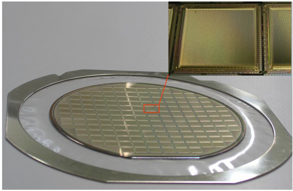
Figure 6.
Silicon CMOS wafer with UV molded cylindrical lenslets after dicing. Detail: selective UV curing leaves the bond pads open for electrical bonding.
3.2. LED Spot Array Illumination
Figure 7a shows a beam shaping device where a lens array is illuminated by a LED in a pupil splitting approach to generate an array of 21 × 21 spots with field-of-view of 40° × 40° [27]. The lens array as the central element was integrated with an aperture array to obscure the space between lenslets. As an additional feature, a buried color filter array was implemented in order to demonstrate the opportunity to color code each individual spot. Apertures and filters were patterned onto blank glass wafers and hard baked before lens replication. A chirped lens array was generated by the approach illustrated in Figure 4 in order to compensate for aberrations of the plano-convex projection lens. Here, the chirp of the microlens position (see Figure 7b) compensates for the distortion while the chirp in the focal length (see Figure 7c) reduces field curvature. As a result we obtained equally spaced spots (period 19 mm) with a distortion <0.5%, and equal spot size of 4 mm [27].
3.3. Multi-Aperture Cameras and Channel Isolation
Multi-aperture imaging concepts implementing microlens arrays are currently investigated to be used as the optics of compact vision sensors for automotive, machine vision, or measurement applications [28]. A main technological difficulty in all multi-aperture systems is the fabrication of features, which serve as channel isolation in order to suppress scattering and optical cross talk which would lead to ghost images. We found that one approach which is compatible to the presented technology is the stacking of thin, plane diaphragm arrays in several layers, with axial separation and diameters designed in a way that scattered light is blocked before impinging upon the adjacent detector. This concept typically involves three different diaphragm layers. Figure 8 shows the cross section of an electronic cluster eye with VGA resolution [29], consisting of an upper wafer with the system aperture stop, as well as an imaging lens array, and the diaphragm stack for channel isolation as the lower part. The diaphragm layers are designed as PSK2000 black matrix polymer layers between thin D263T glass substrates laminated on top of each other using UV curing glue (OG146, Epoxy Technology, Billerica, MA, USA). Chirped lens arrays were generated on the upper wafer for a channel-wise minimization of aberrations. Figure 9 represents measured lens radii across several chips on the wafer. It can be seen that even subtle changes in the design radius (to compensate for field curvature) can be precisely generated—defined by mask 2 of the process described in Figure 4.
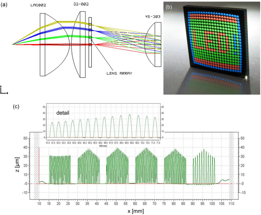
Figure 7.
LED illuminated array of 21 × 21 spots (a) configuration consisting of LED, condenser, chirped lens array and relay lens; (b) photograph of a separated chirped lens array including apertures and filters; (c) measured surface profile across a regular array and chirped arrays. Detail resolves single lenslets.
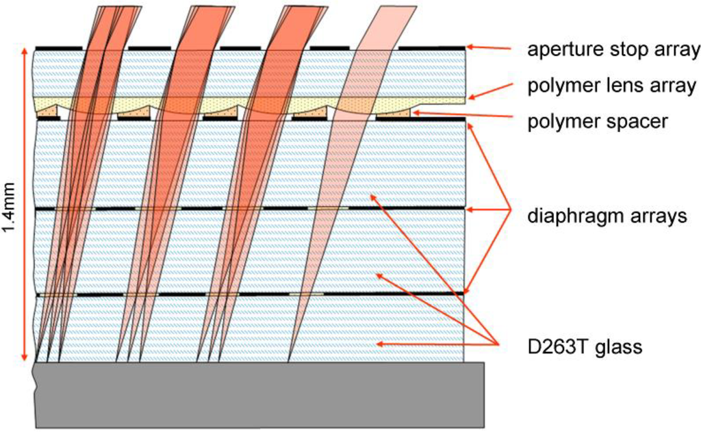
Figure 8.
Schematic cross section of a multiaperture imaging system with VGA resolution.
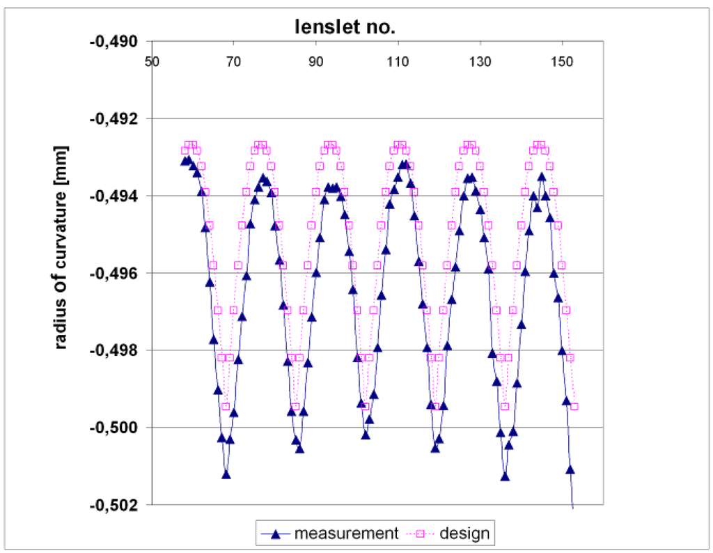
Figure 9.
Chirped lens arrays: Design (hollow squares) and measurement data (full triangles) of lens radii across a row of chips.
A spacer layer was generated on top of the lenses by selective UV molding and subsequent rinsing of uncured resin so that the openings correspond to the optically active areas of the lenslets (see Figure 8). The spacer surface was then coated with a thin layer of UV curing adhesive before upper and lower parts were loaded into the mask-aligner, aligned in x, y direction, brought into contact (z = 0) and bonded together by diffuse UV exposure. The thickness of the bonding adhesive in this example was below 3 µm in order to avoid the lenses being contaminated with excess material, and to achieve the desired axial accuracy of the stack. On the other hand, the adhesive layer was thick and homogenous enough to form tight cavities for each lens, which were not affected in the dicing process. For testing purposes, the optics and imager (without cover glass) were mounted on a chip scale after dicing. Proper focusing within about ±10 µm was achieved solely by the control of lens radii and glass and polymer spacer thickness.
4. Summary and Conclusions
In the present paper we describe a technology for the generation of hybrid-integrated micro-optical systems on wafer scale. Polymer on glass UV molding of microlenses, diffractive elements, or other structures in a specially equipped eight-inch mask aligner combines precision and cost-effective fabrication via replication. The demonstrated high lateral accuracy of ~1 µm is essential for the wafer-scale approach and is suitable for applications where the precise matching to the pitch of detector or fiber arrays is required. Compared to all-polymer technology (like injection molding) the elements show considerably higher stability and lower lateral CTE.
We demonstrated that fabricating a variety of rather complex systems becomes feasible by using UV molding, precise float glass or silicon wafers, dielectric or metal coating, and lithography as patterning and mastering technologies. The process is completed by wafer stacking and dicing. Figure 10 represents a block diagram showing numerous examples, which were realized using this technology. Every example, (a) to (u), is presented as schematic cross sectional view, and a typical application is mentioned. As discussed above, the diversity of systems can be generated because of the compatibility of molding, coating, and lithographical patterning processes. Current technological parameters of our processes are summarized in Table 1.
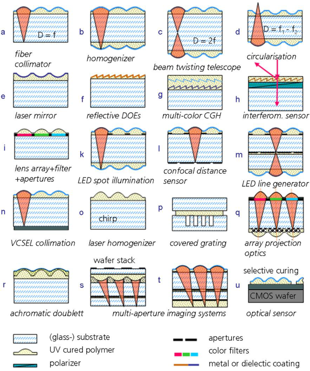
Figure 10.
Survey of realized micro-optical modules shown as schematic cross section.
Mastering and patterning by means of lithography is especially useful when complex layout information has to be processed, as in the case of diffractive elements, (chirped or stochastic) microlenses, aperture or filter arrays and their repetition on the wafer, and additional structures like alignment and dicing marks, test and control structures, etc.
Microlenses mastered by photoresist reflow show diffraction limited performance in a wide parameter range (see Table 1). RIE assisted mastering can extend the design rules towards 100% fill factor of arrays, which was shown for the first time. We demonstrated the feasibility of aspheres and achromatic doublets and their benefits in multi-aperture imaging systems. However, reflow lenses show limited homogeneity of their focal length across the wafer (~1%, see also Figure 2), which causes problems beyond VGA imaging resolution. As a possible alternative, ultra precision machined lens masters with higher accuracy and uniformity, larger size and more complex profiles of the single lenslet can be introduced to the wafer-level concept [5], e.g., by generation of large-area UP machined lens arrays [30,31] or step and repeat replication of a single lenslet in the tooling process. Further extensions of the technology could be the implementation of mechanical actuators or OLED illumination.

Table 1.
Summary of essential technology parameters and typical values realized.
| Parameter | Value | Remark |
|---|---|---|
| lenslet master structure | spherical, elliptical, cylindrical | refined photoresist reflow technology |
| lateral size of lenslet | 10 µm to several millimeters | |
| gap between lenslets | >1 µm | no gap with RIE assisted master |
| lens sag | <200 µm, virtually no minimum | diffraction limited: <100 µm |
| wafer size | Ø200 mm, 150 mm, 100 mm, die | 200 mm × 200 mm also possible |
| wafer thickness | 0.15 nm to 10 mm | Ø200 mm: d > 0.4 mm |
| glass thickness variation | <10 µm total (TTV) | i.e., D263T or B33 (Schott) |
| mask-aligner | MA8e/ SUSS Microtec | closed loop piezo z axis control |
| top-/ bottom side alignm. | Yes | assisted alignment possible |
| lateral alignment/ posit. | ±1 µm | maximum BSA distance 6 mm |
| axial alignment/ position | ±5 µm to (±10 µm) | depending on substrates etc. |
| polymer material | UV curing acrylate or epoxy | i.e., inorganic-organic hybrids [6] |
| temperature stability | >180 °C for ORMOCOMP [5] | 270 °C for t <2 min |
| polymer index/Abbe# | 1.45 to 1.65/60 to 25 | commercial UV curing resin |
| thermo-optical coefficient | −0.00024 K−1 | ORMOCOMP® hybrid polymer |
| polymer thickness | typically 10 µm to 300 | matching the sag limit of reflow lenslets |
| transmission range | 400 nm to 1700 nm | - |
| black aperture resolution | CD ~10 µm (PSK2000, Brewer) | T < 0.1%, R < 5% (300 nm to 700 nm) |
| dicing/ maximum size | thickness <6 mm, Ø < 300 mm | DISCO DAD3350 |
Acknowledgments
Part of this work has been funded by the German Federal Ministry of Education and Research (BMBF) within the projects ”Insect inspired imaging” and “Consumer Micro Camera”.
Furthermore, the authors like to express their gratitude to Sylke Kleinle and Antje Oelschlaeger who participated in the fabrication of the microoptics modules.
Author Contributions
Frank Wippermann and Andreas Brückner were mainly involved in design, technology concepts and optical characterization of multi-aperture imaging, Peter Schreiber for illumination systems. Peter Dannberg and André Matthes did element design, experiments, process development, and geometrical characterization. Andreas Bräuer conceived microoptical systems concepts, coordinated design and technology interactions and approved the final manuscript. All authors discussed the results and commented on the manuscript.
Conflicts of Interest
The authors declare no conflict of interest.
References
- Zwiers, R.J.M.; Dortant, G.C.M. Aspherical lenses produced by a fast high-precision replication process using UV-curable coatings. Appl. Opt. 1985, 24, 4483–4488. [Google Scholar] [CrossRef]
- Dannberg, P.; Erdmann, L.; Bierbaum, R.; Krehl, A.; Bräuer, A. Micro-optical elements and their integration to glass and optoelectronic wafers. Microsyst. Technol. 1999, 1, 41–47. [Google Scholar]
- Rossi, M.; Rudmann, H.; Marty, B.; Maciossek, A. Wafer-Scale Micro-Optics Replication Technology. In Proceedings of Optical Science and Technology, SPIE’s 48th Annual Meeting International Society for Optics and Photonics, San Diego, CA, USA, 4 November 2003; pp. 148–154.
- Jeong, H.S.; Kim, S.H.; Shin, D.I.; Lee, S.C.; Jin, Y.S.; Noh, J.E.; Oh, H.R.; Lee, K.U. Camera imaging lens fabrication using wafer-scale UV embossing process. J. Opt. Soc. KR. 2006, 10, 124–129. [Google Scholar] [CrossRef]
- Dagan, Y. Wafer-Level Optics Enables Low Cost Camera Phones. In Proceedings of SPIE, San Jose, CA, USA, 24 January 2009; Volume 7218, pp. 1–8.
- Hybrid polymers commercially. Available online: http://www.microresist.de/products/ormocers/overview_ormocers_en.htm (accessed on 26 March 2014).
- Rose, K.; Wolter, H.; Glaubitt, W. Multifunctional Acrylate Alkoxysilanes for Polymeric Materials. In Proceedings of MRS, Pittsburgh, PA, USA, January 1992; Volume 271, pp. 731–734.
- Schulz, U.; Schallenberg, U.B.; Kaiser, N. Antireflective coating design for plastic optics. Appl. Opt. 2003, 42, 1346. [Google Scholar] [CrossRef]
- Gentle, T.E.; Schmidt, R.G.; Naasz, B.M.; Gellman, A.J.; Gentle, T.M. Organofunctional silanes as adhesion promoters direct characterization of the polymer/silane interphase. J. Adhes. Sci. Technol. 1992, 6, 307–316. [Google Scholar] [CrossRef]
- Liston, E.M.; Martinu, L.; Wertheimer, M.R. Plasma Surface Modification of Polymers for Improved Adhesion: A Critical Review. In Plasma Surface Modification of Polymers Relevance to Adhesion; Strobel, M., Lyons, C., Mittal, K.L., Eds.; VSP BV: Utrecht, the Netherlands, 1994; pp. 3–39. [Google Scholar]
- Kämpfe, T.; Kley, E.B.; Tünnermann, A.; Dannberg, P. Design and fabrication of stacked computer generated holograms for multicolour image generation. Appl. Opt. 2007, 46, 5482–5488. [Google Scholar] [CrossRef]
- Stollberg, K.; Brückner, A.; Duparré, J.; Dannberg, P.; Bräuer, A.; Tünnermann, A. The Gabor super lens as an alternative wafer-level camera approach inspired by superposition compound eyes of nocturnal insects. Opt. Express 2009, 17, 15747–15759. [Google Scholar]
- Popovich, Z.D.; Sprague, R.A.; Conell, G.A.N. Technique for monolithic fabrication of microlens arrays. Appl. Opt. 1988, 27, 1281–1284. [Google Scholar] [CrossRef]
- Daly, D.; Stevens, R.F.; Hutley, M.C.; Davies, N. The manufacture of microlenses by melting photoresist. J. Meas. Sci. Technol. 1990, 1, 759–766. [Google Scholar] [CrossRef]
- Lim, C.H.; Jeung, W.K.; Choi, S.M. LED Packaging Using High Sag Rectangular Microlens Array. In Proceedings of SPIE 6185, Micro-Optics, VCSELs, and Photonic Interconnects II: Fabrication, Packaging and Integration, Strasbourg, France, 21 April 2006; Volume 618516. [CrossRef]
- Zeitner, U.D.; Dannberg, P. Double-Sided Hybrid Microoptical Elements Combining Functions of Multistage Optical Systems. In Proceedings of SPIE 4440, Lithographic and Micromachining Techniques for Optical Component Fabrication, San Diego, CA, USA, 9 November 2011; Volume 44. [CrossRef]
- Wippermann, F.; Zeitner, U.D.; Dannberg, P.; Bräuer, A.; Sinzinger, S. Beam homogenizers based on chirped microlens arrays. Opt. Express 2007, 15, 6218–6223. [Google Scholar]
- Duparré, J.; Wippermann, F.; Dannberg, P.; Reimann, A. Chirped arrays of refractive ellipsoidal microlenses for aberration correction under oblique incidence. Opt. Express 2009, 13, 10539–10551. [Google Scholar]
- Schreiber, P.; Dannberg, P.; Hoefer, B.; Beckert, E. Chirped Microlens Arrays for Diode Laser Circularization and Beam Expansion. In Proceedings of SPIE 5876, Laser Beam Shaping VI, San Diego, CA, USA, 30 August 2005; Volume 58760K. [CrossRef]
- Wippermann, F.; Radtke, D.; Zeitner, U.; Duparré, J.W.; Tünnermann, A.; Amberg, M.; Sinzinger, S.; Reinhardt, C.; Ovsianikov, A.; Chichkov, B.N. Fabrication Technologies for Chirped Refractive Microlens Arrays. In Proceedings of SPIE 6288, Current Developments in Lens Design and Optical Engineering VII, San Diego, CA, USA, 31 August 2006; Volume 62880O. [CrossRef]
- Nussbaum, P.; Völkel, R.; Herzig, H.P.; Eisner, M.; Haselbeck, S. Design fabrication and testing of microlens arrays for sensors and microsystems. Pure Appl. Opt. 1997, 6, 617–636. [Google Scholar]
- Voelkel, R.; Eisner, M.; Weible, K. Fabrication of Aspherical Microlenses in Fused Silica and Silicon. In Proceedings of SPIE 4440, Lithographic and Micromachining Techniques for Optical Component Fabrication, San Diego, CA, USA, 9 Novmber 2001; Volume 40. [CrossRef]
- Harding, R.; Gardiner, I.; Yoon, H.J.; Perrett, T.; Parri, O.; Skjonnem, K. Reactive Liquid Crystal Materials for Optically Anisotropic Patterned Retarders. In Proceedings of SPIE Lithography Asia, Taipei, Taiwan, 4 December 2008; Volume 71402J. [CrossRef]
- CODIXX standard polarizer products. Available online: http://www.codixx.de/cms/polarizers/polarizer.html (accessed on 26 March 2014).
- Albero, J; Bargiel, S.; Passilly, N.; Dannberg, P.; Stumpf, M; Zeitner, U.D.; Rousselot, C.; Gastinger, K.; Goreck, C. Micromachined array-type mirauinterferometer for parallel inspection of MEMS. J. Micromech. Microeng. 2011, 21, 065005. [Google Scholar] [CrossRef]
- Kim, S.M.; Kim, H.M.; Kang, S. Development of an ultraviolet imprinting process for integrating a microlens array onto an image sensor. Opt. Lett. 2006, 31, 10–12. [Google Scholar]
- Schreiber, P.; Dannberg, P.; Wippermann, F. Chirped Lens-Array LED Spot-Array Generator with Individually Colored Spots. In Proceedings of SPIE 7716, Micro-Optics 2010, Brussels, Belgium, 13 May 2010; Volume 771617. [CrossRef]
- Duparré, J.; Wippermann, F. Micro-optical artificial compound eyes. Bioinsp. Biomim. 2006, 1, R1. [Google Scholar] [CrossRef]
- Brückner, A.; Duparré, J.; Dannberg, P.; Leitel, R.; Bräuer, A. Driving Microoptical Imaging Systems Towards Miniature Camera Applications. In Proceedings of SPIE 7716, Micro-Optics 2010, Brussels, Belgium, 12 May 2010; Volume 77160J. [CrossRef]
- Rømer Holme, N.C.; Geltzer Dinesen, P.; Attar, Z.; Oliver, S.D.; Voelkel, R. New technologies enable precise and cost effective waferlevel optics. Laser Focus World 2009, 37, 87–90. [Google Scholar]
- Wafer-level optics tooling. Available online: http://www.kaleido-technology.com/Applications/Wafer-level%20optics%20tooling.pdf (accessed on 26 March 2014).
© 2014 by the authors; licensee MDPI, Basel, Switzerland. This article is an open access article distributed under the terms and conditions of the Creative Commons Attribution license (http://creativecommons.org/licenses/by/3.0/).