
A Monolithic 3-Dimensional Static Random Access Memory Containing a Feedback Field Effect Transistor


ICT & Robotics Engineering, Semiconductor Convergence Engineering, AISPC Laboratory, IITC, Hankyong National University, 327 Jungang-ro, Anseong-si 17579, Gyenggi-do, Korea
*
Author to whom correspondence should be addressed.
Micromachines 2022, 13(10), 1625; https://doi.org/10.3390/mi13101625
Submission received: 28 August 2022
/
Revised: 10 September 2022
/
Accepted: 27 September 2022
/
Published: 28 September 2022
(This article belongs to the Special Issue NANO KOREA 2022)
Abstract
:A monolithic three-dimensional integrated static random access memory containing a feedback field effect transistor (M3D-FBFET-SRAM) was proposed. The M3D-FBFET-SRAM cell consists of one metal oxide semiconductor field effect transistor (MOSFET) and one FBFET, and each transistor is located on the top tier and one on the bottom tier in a monolithic 3D integration, respectively. The electrical characteristics and operation of the NFBFET in the M3D-FBFET-SRAM cell were investigated using a TCAD simulator. For SRAM operation, the optimum doping profile of the NFBFET was used for non-turn-off characteristics. For the M3D-FBFET-SRAM cell, the operation of the SRAM and electrical coupling occurring between the top and bottom tier transistor were investigated. As the thickness of interlayer dielectric decreases, the reading ‘ON’ current decreases. To prevent performance degradation, two ways to compensate for current level were suggested.
1. Introduction
Over the past few decades, computing systems have followed the von Neumann architecture [1]. An important feature in this architecture is the data process. The processed data are transferred from a processing unit to a memory unit. Throughout this process, intermediate memory storage is necessary. In the current computing systems, the volatile type of memory circuits that maintain data when the supply voltage is applied are configured close to the processing unit. Static random access memory (SRAM) is designed for the nearest processing unit because it performs very rapidly and does not need to be refreshed [2]. The conventional SRAM cell has two access transistors and two inverters, which consist of two transistors. Due to the SRAM circuit configuration, the cache memory made up of SRAM occupies a large portion of the overall processor chip. For designing next-generation processor chips, it is necessary to improve the performance and reduce the area of the SRAM.
A monolithic three-dimensional (M3D) integration is one of fabrication technologies for overcoming Moore’s Law [3,4,5,6,7,8,9]. The circuits with M3D structure are designed vertically for the transistor, logic gates, and system level. The circuit designed with M3D technology exhibits a high integration of the transistors and has a low propagation delay due to vertical interconnection. In order to utilize these characteristics, various circuits with the M3D structure were studied [10,11,12,13,14,15,16]. Particularly, the 6T (or more than six transistors) SRAMs with M3D structure have been proposed and studied to increase density, which can achieve up to a 45% density increase [17,18,19,20,21,22].
To improve the performance, density, and power consumption of SRAM, the configurations of SRAM with novel devices are introduced [23,24,25]. Among these, a feedback field effect transistor (FBFET) has been attracting attention for use in a next-generation memory device due to its steep slope and hysteresis characteristics [26]. Moreover, various memory circuits containing the FBFET have been proposed because the FBFET can be fabricated with a complementary MOS (CMOS) process. The SRAM consisting of one FBFET and one MOSFET (FBFET-SRAM) was proposed [27]. The density and power dissipation of FBFET-SRAM cell are improved more than those of the conventional 6T-SRAM. The FBFET-SRAM can be stacked vertically with the M3D structure because the devices used in the FBFET-SRAM, such as fully depleted silicon on insulator (FDSOI) FET, FBFET, junctionless FET, tunnel FET, gate-all-around FET, and nanosheet FET, are stackable. Therefore, there is a need for research on FBFET-SRAM with M3D structure (M3D-FBFET-SRAM) cells to meet the high density demands.
In this study, the M3D-FBFET-SRAM cell is proposed, and its electrical characteristics are investigated using technology computer aided design (TCAD). First, the simulation structure of the M3D-FBFET-SRAM cell is described in Section 2. In Section 3, the electrical characteristics of the M3D-FBFET-SRAM cell regarding DC characteristics and cell operation are discussed. In Section 4, the electrical coupling occurring at the top tier transistor is discussed. Finally, the conclusions of this study are described.
2. Simulation Structure
Figure 1a–c show the three-dimensional bird’s eyes view of the M3D-FBFET-SRAM cell, the process sequence, and a cross-section of the A-A` and circuit diagram of the M3D-FBFET-SRAM cell, respectively. The M3D-FBFET-SRAM cell consists of N-type FBFET (NFBFET) and N-type MOSFET (NMOSFET), and the NFBFET and NMOSFET are located on bottom tier and top tier, respectively. The material compositions and doping profile for the M3D-FBFET-SRAM cell were described, as shown in Figure 1a. The work-function of gate metal was used for 5.0 eV at NFBFET and NMOSFET. The device widths are 160 nm and 80 nm for the NFBFET and NMOSFET, respectively. The M3D-FBFET-SRAM cell was fabricated using a Victory Process simulator [28], and the electrical characteristics of the M3D-FBFET-SRAM cell were investigated using the commercial TCAD simulation program Atlas in mixed-mode [29]. The fabrication process was based on FDSOI technology [30] for the bottom and top tier transistors. In particular, the fabrication of the top tier transistor requires a low temperature in the monolithic fabrication technology due to interlayer dielectric (ILD) [31]. Therefore, the low temperature was used during the deposition, ion implantation, and annealing process, as shown in Figure 1b. Table 1 shows the structure parameters of the M3D-FBFET-SRAM cell. The physical models including CVT, SRH, and FERMI for NMOSFET, as well as CONMOB, FLDMOB, CONSRH, AUGER, and BGN for NFBFET, were used for simulation.
3. Simulation Results
In this section, the electrical characteristics of the M3D-FBFET-SRAM cell will be discussed. First, the operation and electrical characteristics of the NFBFET were investigated with respect to the energy band diagram. Moreover, during the writing operation of the M3D-FBFET-SRAM cell, the role of NFBFET was investigated. Based on the NFBFET operation, the M3D-FBFET-SRAM cell operation was investigated, particularly, due to the M3D structure, the electrical coupling occurring between the top and bottom tier transistors [32]. This coupling effect causes the electrical characteristics of the top tier transistor to change. Therefore, the investigation of the electrical coupling was conducted.
3.1. Electrical Characteristics of the NFBFET in the M3D-FBFET-SRAM Cell
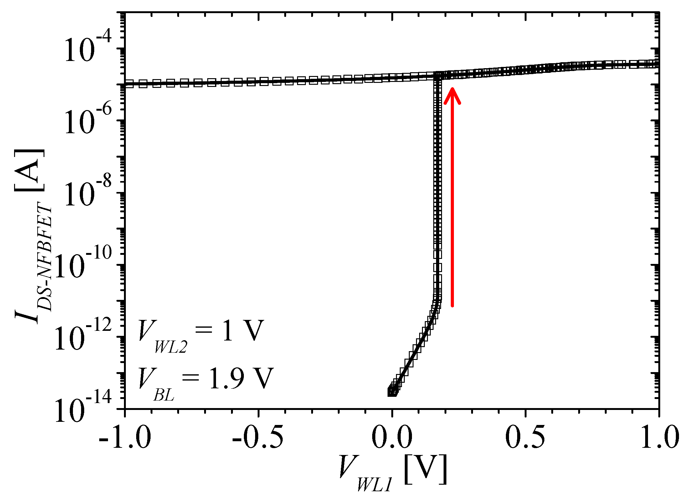
Figure 2a–c shows the energy band diagram of the NFBFET under three different bias conditions. The red and black lines denote the conduction band and valence band, respectively. For the initial state of the NFBFET, the bit line voltage (VBL) and word line 2 voltage (VWL2) are applied with 1.9 V and 1 V, respectively. At this state, the electrons from the source region cannot be injected into the channel region, due to the potential barrier at the gated channel region, as shown in Figure 2a. When the forward sweep starts at the word line 1 voltage (VWL1), the potential barrier is lowering, and the electrons drift into the ungated channel region by the drain-source field. The injected electrons accumulate at the potential well at the ungated channel region; thereafter, the potential well is eliminated by accumulated electrons. The holes from the drain region can diffuse by the lowered potential barrier at the ungated channel region, and accumulate at the gated channel region, as shown in Figure 2b. Finally, this positive feedback between the electrons and the holes injection causes the energy band of all the regions align, as shown in Figure 2c. Figure 3 shows the drain-source current of the NFBFET (IDS-NFBFET) versus VWL1. There is an abrupt increment of the NFBFET current at VWL1 = 0.17 V. The hysteresis characteristic, which is the threshold voltage difference between forward and reverse, can be controlled by the doping profile of the channel region [33]. For the FBFET-SRAM operation, the very large memory window or non-turn-off characteristics by the gate-field, are required for maintaining the reading ‘ON’ current level, as shown in Figure 3. The doping profile is adjusted to satisfy the performance of NFBFET.
Figure 4a,b shows the NFBFET current (IDS-NFBFET) for writing the ‘ON’ and ‘OFF’ operation in the M3D-FBFEET-SRAM cell, respectively. The red line and black square-lines denote the operation current and DC characteristics of the NFBFET, respectively. When the writing ‘ON’ operation begins, VBL, VWL1, and VWL2 are applied for 1.9 V, 0.6 V, and 1.0 V, respectively. When the writing ‘ON’ pulse is applied to the M3D-FBFET-SRAM cell, the NFBFET currents change following the blue arrows, as shown in Figure 4a. When the writing ‘OFF’ operation begins, VBL, VWL1, and VWL2 are applied for 0.7 V, 0.6 V, and 1.0 V, respectively. When the writing ‘OFF’ pulse is applied to the SRAM cell, the NFBFET current changes following the blue arrows, as shown in Figure 4b.
3.2. M3D-FBFET-SRAM Cell Operation
Figure 5 shows the timing diagram of the M3D-FBFET-SRAM cell operation. The black, blue, green, and red lines denote the voltage pulse of VBL, VWL1, and VWL2, and the current pulse of IDS-NFBFET, respectively. Table 2 shows the M3D-FBFET-SRAM cell operation voltages. The rising, falling, and pulse-width times are 0.2 ns [27]. For the reading ‘ON’ and ‘OFF’ currents, IDS-NFBFET are approximately 15 μA and 0.2 nA, respectively. The writing ‘ON’ and ‘OFF’ speeds are about 0.4 ns, as shown in Figure 5. For the first suggested FBFET-SRAM, the unit cell size is 8F2 (F = feature size) [27], and this cell achieves very high density compared with conventional 6T-SRAM. However, when the FBFET-SRAM is designed with the M3D structure, the cell area can decrease up to 50% compared with the planer 2-D cell structure [27].
Figure 6a,b show the retention characteristics of the M3D-FBFET-SRAM cell when the recursive reading pulse is applied after the writing ‘ON’ and ‘OFF’ operations, respectively. For investigating the retention characteristics of the M3D-FBFET-SRAM cell, the retention time was 30,000 s. When the NFBFET is turned on, the NFBFET remains in the on-state until it has formed the potential well in the channel region. For maintaining the on-state, the NFBFET requires appropriate IDS-NFBFET, which can be controlled by holding voltages of VWL2 [27]. As shown in Figure 6a,b, the M3D-FBFET-SRAM cell maintains the data for 30,000 s after the writing ‘ON’ and ‘OFF’ operations, respectively.
3.3. Electrical Coupling
For the M3D structure, the electrical characteristics of the top tier transistor can be changed by the thickness of the interlayer dielectric (TILD). As TILD decreases, the electric field occurring at the bottom tier transistor effects the top tier transistor. This coupling effect causes unexpected changes in system performance. In order to design the system with intended performance, the investigation for changing the electrical characteristics must be proceeded with respect to TILD. In this section, the electrical coupling occurring between the top and bottom transistors was investigated. Furthermore, the optimum voltages were suggested for short TILD.
Figure 7a shows the drain-source current of the NMOSFET (IDS-NMOSFET), which is located in the top tier, at TILD = 3 nm. The red and black lines denote IDS-NMOSFET at VWL1 = 0.6 and 0 V, respectively. As TILD decreases, the electric field applied to the top tier transistor is stronger. When VWL1 is applied for 0.6 V, the threshold voltages of IDS-NMOSFET changes from 0.67 V (for VWL1 = 0 V) to 0.50 V, as shown in Figure 7a. Figure 7b shows the M3D-FBFET-SRAM cell operation at various TILD. As TILD decreases, the threshold voltage of IDS-NMOSFET decreases and IDS-NMOSFET increases at the same VWL2. The current level (IDS-NFBFET) must be lower to match the current levels of the NFBFET and the NMOSFET by their serial connection; thus, VA must also be reduced, as shown in Figure 1c. Therefore, as TILD decreases, the reading ‘ON’ currents decrease in the direction of the orange arrow, as shown in Figure 7b.
Figure 8a,b shows the reading ‘ON’ current of the M3D-FBFET-SRAM cell with TILD = 3 nm at modified VBL and VWL2, respectively. The black and red lines denote IDS-NFBFET with original and modified voltage levels, respectively. To design the M3D-FBFET-SRAM with shorter TILD, it is necessary to solve the problem of lowering the reading ‘ON’ current, because the low reading ‘ON’ current is a critical problem in SRAM operation. To solve this problem, higher VBL and VWL2 can be chosen to create a high reading ‘ON’ current, as shown in Figure 8a,b. The shorter TILD can achieve a lower critical delay due to shorter monolithic inter-tier via the TILD. However, higher voltage levels of VBL and VWL2 are required, and power consumption will be high. In order to design the M3D-FBFET-SRAM, the appropriate TILD must be investigated for an acceptable trade-off regarding the performance.
4. Conclusions
In this study, the M3D-FBFET-SRAM cell was proposed. The M3D-FBFET-SRAM cell consists of one NFBFET and one NMOSFET, and the NFBFET and NMOSFET in the M3D structure are located on the bottom and top tier, respectively. The transistors are stacked vertically; therefore, the M3D-FBFET-SRAM cell area achieved up to a 50% reduction compared with 2-D planer cell structure. The electrical characteristics of the M3D-FBFET-SRAM were investigated. First, for the NFBFET, the DC characteristics and role were investigated during the writing operation. In order to achieve the non-turn-off characteristics, the optimum doping profile of the NFBFET was used. Based on the NFBFET operation, the M3D-FBFET-SRAM cell operation was investigated. The reading ‘ON’ and ‘OFF’ current are approximately 15 μA and 0.2 nA, respectively. For the retention characteristics, the M3D-FBFET-SRAM cell can maintain the data for at least 30,000 s. In particular, the electrical coupling occurring between the top and bottom transistors was investigated with respect to TILD. As TILD decreases, the reading ‘ON’ current decreases. To compensate for the reading ‘ON’ current, a higher VBL and VWL2 can be applied; however, the power consumption will be higher. Therefore, in order to design the M3D-FBFET-SRAM, the investigation of the appropriate TILD must be conducted.
Author Contributions
Conceptualization, J.H.O. and Y.S.Y.; methodology, J.H.O. and Y.S.Y.; investigation, J.H.O. and Y.S.Y.; data curation, J.H.O.; writing—original draft preparation, J.H.O.; writing—review and editing, J.H.O. and Y.S.Y.; supervision, Y.S.Y.; project administration, Y.S.Y.; funding acquisition, Y.S.Y. All authors have read and agreed to the published version of the manuscript.
Funding
This research was supported by the Basic Science Research Program through NRF of Korea, funded by the Ministry of Education (NRF-2019R1A2C1085295).
Acknowledgments
This work was supported by IDEC (EDA tool).
Conflicts of Interest
The authors declare no conflict of interest.
References
- Jaiswal, A.; Chakraborty, I.; Agrawal, A.; Roy, K. 8T SRAM Cell as a Multibit Dot-Product Engine for Beyond Von Neumann Computing. IEEE Trans. Very Large Scale Integr. Syst. 2019, 27, 2556–2567. [Google Scholar] [CrossRef]
- Lee, C.-F.; Lu, C.-H.; Lee, C.-E.; Mori, H.; Fujiwara, H.; Shih, Y.-C.; Chou, T.-L.; Chih, Y.-D.; Chang, T.-Y.J. A 12 nm 121-TOPS/W 41.6-TOPS/mm2 all digital full precision SRAM-based compute-in-memory with configurable bit-width for AI edge applications. In Proceedings of the 2022 IEEE Symposium on VLSI Technology and Circuits (VLSI Technology and Circuits), Honolulu, HI, USA, 12–17 June 2022; pp. 24–25. [Google Scholar]
- Wong, S.; El-Gamal, A.; Griffin, P.; Nishi, Y.; Pease, F.; Plummer, J. Monolithic 3D integrated circuits. In Proceedings of the 2007 International Symposium on VLSI Technology, Systems and Applications (VLSI-TSA), Hsinchu, Taiwan, 23–25 April 2007; pp. 1–4. [Google Scholar]
- Liu, C.; Lim, S.K. A design tradeoff study with monolithic 3D integration. In Proceedings of the Thirteenth International Symposium on Quality Electronic Design (ISQED), Santa Clara, CA, USA, 19–21 March 2012; pp. 529–536. [Google Scholar]
- Panth, S.; Samal, S.; Yu, Y.S.; Lim, S.K. Design challenges and solutions for ultra-high-density monolithic 3D ICs. In Proceedings of the 2014 SOI-3D-Subthreshold Microelectronics Technology Unified Conference (S3S), Millbrae, CA, USA, 6–9 October 2014; pp. 1–2. [Google Scholar]
- Park, J.-H.; Tada, M.; Kuzum, D.; Kapur, P.; Yu, H.-Y.; Philip Wong, H.-S.; Saraswat, K.C. Low temperature (≤380 °C) and high performance Ge CMOS technology with novel source/drain by metal-induced dopants activation and high-k/metal gate stack for monolithic 3D integration. In Proceedings of the 2008 IEEE International Electron Device Meeting (IEDM), San Francisco, CA, USA, 15–17 December 2008; pp. 1–4. [Google Scholar]
- Vinet, M.; Batude, P.; Fenouillet-Beranger, C.; Clermidy, F.; Brunet, L.; Rozeau, O.; Hartmannn, J.M.; Billoint, O.; Cibrario, G.; Previtali, B.; et al. Monolithic 3D integration: A powerful alternative to classical 2D scaling. In Proceedings of the 2014 SOI-3D-Subthreshold Microelectronics Technology Unified Conference (S3S), Millbrae, CA, USA, 6–9 October 2014; pp. 1–3. [Google Scholar]
- Nayak, D.K.; Banna, S.; Samal, S.K.; Lim, S.K. Power, performance, and cost comparisons of monolithic 3D ICs and TSV-based 3D ICs. In Proceedings of the 2015 IEEE SOI-3D-Subthreshold Microelectronics Technology Unified Conference (S3S), Rohnert Park, CA, USA, 5–8 October 2015; pp. 1–2. [Google Scholar]
- Panth, S.; Samadi, K.; Du, Y.; Lim, S.K. High-density integration of functional modules using monolithic 3D-IC technology. In Proceedings of the 2013 18th Asia and South Pacific Design Automation Conference (ASP-DAC), Yokohama, Japan, 22–25 January 2013; pp. 681–686. [Google Scholar]
- Lee, Y.-J.; Lim, S.K. Ultrahigh density logic designs using monolithic 3-D integration. IEEE Trans. Comput.-Aided Des. Integr. Circuits Syst. 2013, 32, 1892–1905. [Google Scholar] [CrossRef]
- Shulaker, M.M.; Wu, T.F.; Pal, A.; Zhao, L.; Nishi, Y.; Saraswat, K.; Philip Wong, H.-S.; Mitra, S. Monolithic 3D integration of logic and memory: Carbon nanotube FETs, resistive RAM, and silicon FETs. In Proceedings of the 2014 IEEE International Electron Devices Meeting (IEDM), San Francisco, CA, USA, 15–17 December 2014. [Google Scholar]
- Lee, G.J.; Ahn, T.J.; Lim, S.K.; Yu, Y.S. Investigation into electrical characteristics of logic circuit consisting of modularized monolithic 3D inverter unit cell. J. Inf. Commun. Converg. Eng. 2022, 20, 137–142. [Google Scholar] [CrossRef]
- Yu, M.-J.; Lin, R.-P.; Chang, Y.-H.; Hou, T.-H. High-voltage amorphous InGaZnO TFT with Al2O3 high-k dielectric for low-temperature monolithic 3-D integration. IEEE Trans. Electron Devices 2016, 63, 3944–3949. [Google Scholar] [CrossRef]
- Jiang, J.; Parto, K.; Cao, W.; Banerjee, K. Ultimate monolithic-3D integration with 2D materials: Rationale, prospects, and challenges. IEEE J. Electron Devices Soc. 2019, 7, 878–887. [Google Scholar] [CrossRef]
- Ahn, T.-J.; Yu, Y.S.; Kim, N.H. Comparison of two-types of monolithic 3D inverter consisting of MOSFETs and junctionless FETs. In Proceedings of the 2020 International Conference on Electronics, Information, and Communication (ICEIC), Barcelona, Spain, 19–22 January 2020; pp. 1–3. [Google Scholar]
- Shulaker, M.M.; Saraswat, K.; Philip Wong, H.-S.; Mitra, S. Monolithic three-dimensional integration of carbon nanotube FETs with silicon CMOS. In Proceedings of the 2014 Symposium on VLSI Technology (VLSI-Technology): Digest of Technical Paper, Honolulu, HI, USA, 9–12 June 2014; pp. 1–2. [Google Scholar]
- Ahn, T.J.; Choi, B.H.; Lim, S.K.; Yu, Y.S. Electrical Coupling and Simulation of Monolithic 3D Logic Circuits and Static Random Access Memory. Micromachines 2019, 10, 637. [Google Scholar] [CrossRef] [PubMed]
- Boumchedda, R.; Noel, J.-P.; Giraud, B.; Akyel, K.C.; Brocard, M.; Turgis, D.; Beigne, E. High-Density 4T SRAM Bitcell in 14-Nm 3-D CoolCube Technology Exploiting Assist Techniques. IEEE Trans. Very Large Scale Integr. Syst. 2017, 25, 2296–2306. [Google Scholar] [CrossRef]
- Batude, P.; Jaud, M.-A.; Thomas, O.; Clavelier, L.; Pouydebasque, A.; Vinet, M.; Deleonibus, S.; Amara, A. 3D CMOS Integration: Introduction of Dynamic Coupling and Application to Compact and Robust 4T SRAM. In Proceedings of the 2008 IEEE International Conference on Integrated Circuit Design and Technology and Tutorial, Grenoble, France, 2–4 June 2008; pp. 281–284. [Google Scholar]
- Srinivasa, S.; Li, X.; Chang, M.-F.; Sampson, J.; Gupta, S.K.; Narayanan, V. Compact 3-D-SRAM memory with concurrent row and column data access capability using sequential monolithic 3-D integration. IEEE Trans. Very Large Scale Integr. Syst. 2018, 26, 671–683. [Google Scholar] [CrossRef]
- Naito, T.; Ishida, T.; Onoduka, T.; Nishigoori, M.; Nakayama, T.; Ueno, Y.; Ishimoto, Y.; Suzuki, A.; Chung, W.; Madurawe, R.; et al. World’s first monolithic 3D-FPGA with TFT SRAM over 90 nm 9 layer Cu CMOS. In Proceedings of the 2010 Symposium on VLSI Technology, Honolulu, HI, USA, 15–17 June 2010; pp. 219–220. [Google Scholar]
- Yu, C.-H.; Su, P.; Chuang, C.-T. Performance and stability benchmarking of monolithic 3-D logic circuits and SRAM cells with monolayer and few-layer transition metal dichalcogenide MOSFETs. IEEE Trans. Electron Devices 2017, 64, 2445–2451. [Google Scholar] [CrossRef]
- Tripathi, S.; Choudhary, S.; Misra, P.K. A novel STT-SOT MTJ-based nonvolatile SRAM for power gating application. IEEE Trans. Electron Devices 2022, 69, 1058–1064. [Google Scholar] [CrossRef]
- Garg, N.; Pratap, Y.; Kabra, S. Stability and reliability performance of double gate junctionless transistor (DG-JLT) 6T SRAM. In Proceedings of the 2021 International Conference on Industrial Electronics Research and Applications (ICIERA), New Delhi, India, 22–24 December 2021; pp. 1–5. [Google Scholar]
- Woo, S.; Cho, J.; Lim, D.; Cho, K.; Kim, S. Transposable 3T-SRAM Synaptic Array Using Independent Double-Gate Feedback Field-Effect Transistors. IEEE Trans. Electron Devices 2019, 66, 4753–4758. [Google Scholar] [CrossRef]
- Padilla, A.; Yeung, C.W.; Shin, C.; Hu, C.; Liu, T.-J.K. Feedback FET: A Novel Transistor Exhibiting Steep Switching Behavior at Low Bias Voltages. In Proceedings of the 2008 IEEE International Electron Devices Meeting (IEDM), San Francisco, CA, USA, 15–17 December 2008; pp. 1–4. [Google Scholar]
- Cho, J.; Lim, D.; Woo, S.; Cho, K.; Kim, S. Static Random Access Memory Characteristics of Single-Gated Feedback Field-Effect Transistors. IEEE Trans. Electron Devices 2019, 66, 413–419. [Google Scholar] [CrossRef]
- Silvaco Int. Victory Process, version 7.58.3. R Manual; Silvaco Int.: Santa Clara, CA, USA, 2021.
- Silvaco Int. ATLAS, version 5.32.1. R Manual; Silvaco Int.: Santa Clara, CA, USA, 2022.
- Lee, K.H.; El-Dirani, H.; Fonteneau, P.; Bawedin, M.; Cristoloveanu, S. Sharp Logic Switch Based on Band Modulation. IEEE Electron Device Lett. 2019, 40, 1852–1855. [Google Scholar] [CrossRef]
- Santos, C.; Vivet, P.; Thuries, S.; Billoint, O.; Colonna, J.-P.; Coudrain, P.; Wang, L. Thermal Performance of CoolCubeTM Monolithic and TSV-Based 3D Integration Processes. In Proceedings of the 2016 IEEE International 3D Systems Integration Conference (3DIC), San Francisco, CA, USA, 8–11 November 2016; pp. 1–5. [Google Scholar]
- Yu, Y.S.; Panth, S.; Lim, S.K. Electrical Coupling of Monolithic 3-D Inverters. IEEE Trans. Electron Devices 2016, 63, 1–4. [Google Scholar] [CrossRef]
- Oh, J.H.; Yu, Y.S. Investigation of monolithic 3D integrated circuit inverter with feedback field effect transistors using TCAD simulation. Micromachines 2020, 11, 852. [Google Scholar] [CrossRef] [PubMed]
Figure 1.
(a) A three−dimensional bird’s eyes view of the M3D−FBFET−SRAM cell, (b) its fabrication process sequence, (c) its cross−section of A-A` and circuit diagram.
Figure 1.
(a) A three−dimensional bird’s eyes view of the M3D−FBFET−SRAM cell, (b) its fabrication process sequence, (c) its cross−section of A-A` and circuit diagram.
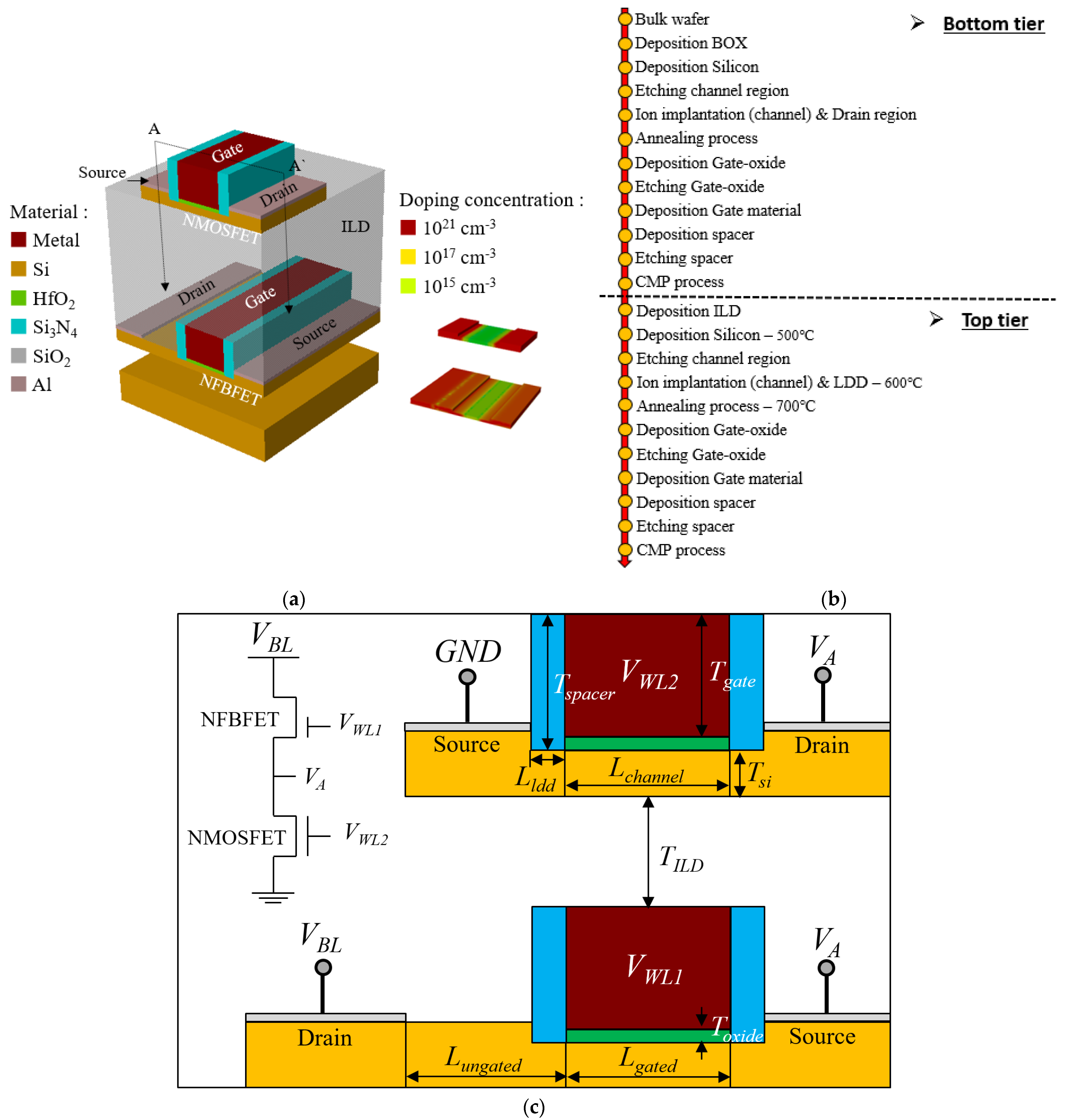
Figure 2.
The energy band diagram of the NFBFET in the M3D−FBFET−SRAM cell. (a) Initial state (VBL = 1.9 V, VWL2 = 1 V, and VWL1 = 0 V), (b) VWL1 forward sweep (VBL = 1.9 V and VWL2 = 1 V), (c) on−state (VBL = 1.9 V and VWL1 = VWL2 = 1 V).
Figure 2.
The energy band diagram of the NFBFET in the M3D−FBFET−SRAM cell. (a) Initial state (VBL = 1.9 V, VWL2 = 1 V, and VWL1 = 0 V), (b) VWL1 forward sweep (VBL = 1.9 V and VWL2 = 1 V), (c) on−state (VBL = 1.9 V and VWL1 = VWL2 = 1 V).
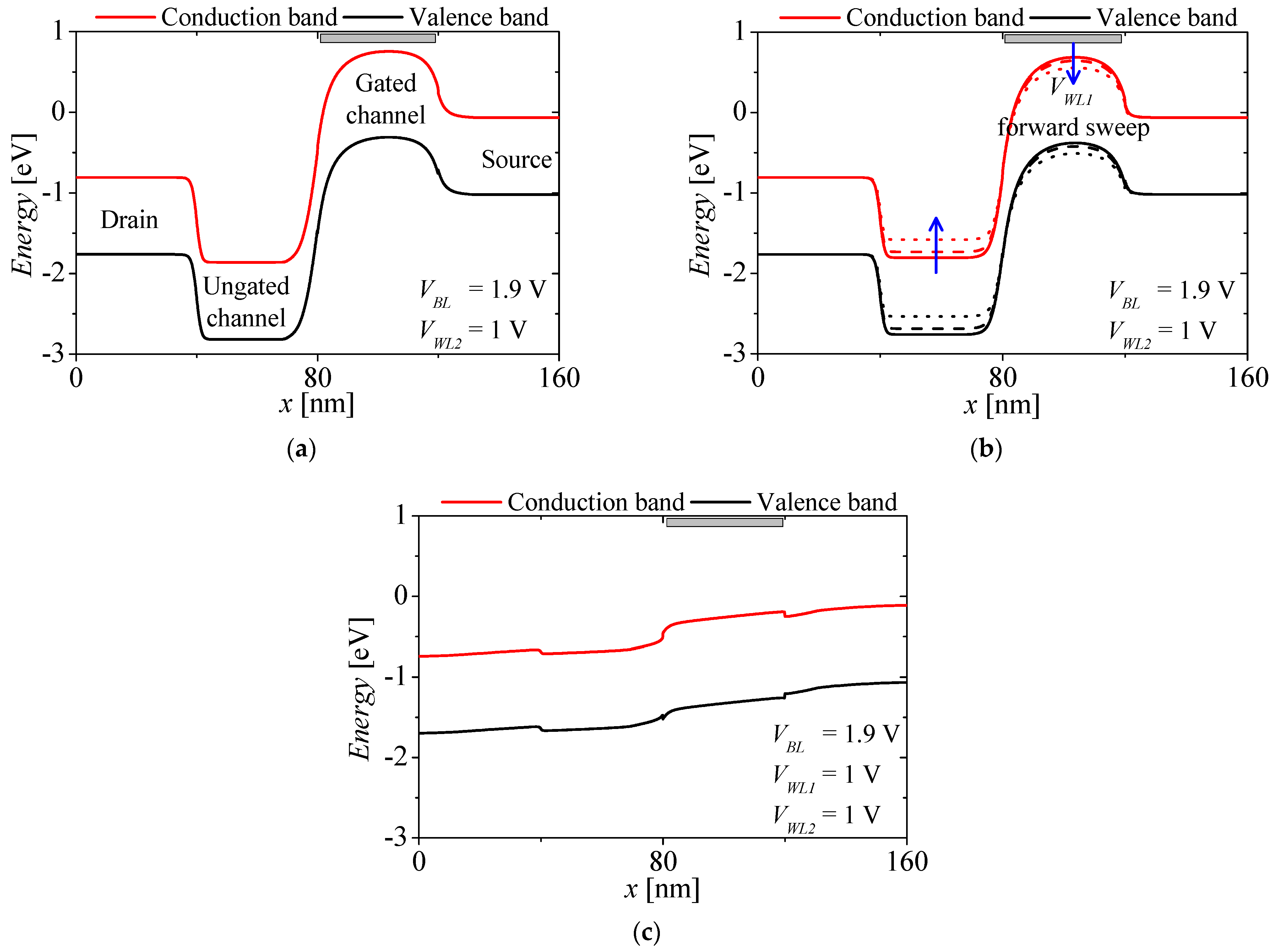
Figure 3.
Drain−source current of the NFBFET (IDS−NFBFET) versus VWL1 when VBL = 1.9 V and VWL2 = 1 V.
Figure 3.
Drain−source current of the NFBFET (IDS−NFBFET) versus VWL1 when VBL = 1.9 V and VWL2 = 1 V.

Figure 4.
The NFBFET current during the (a) writing ‘ON’ operation and (b) writing ‘OFF’ operation.
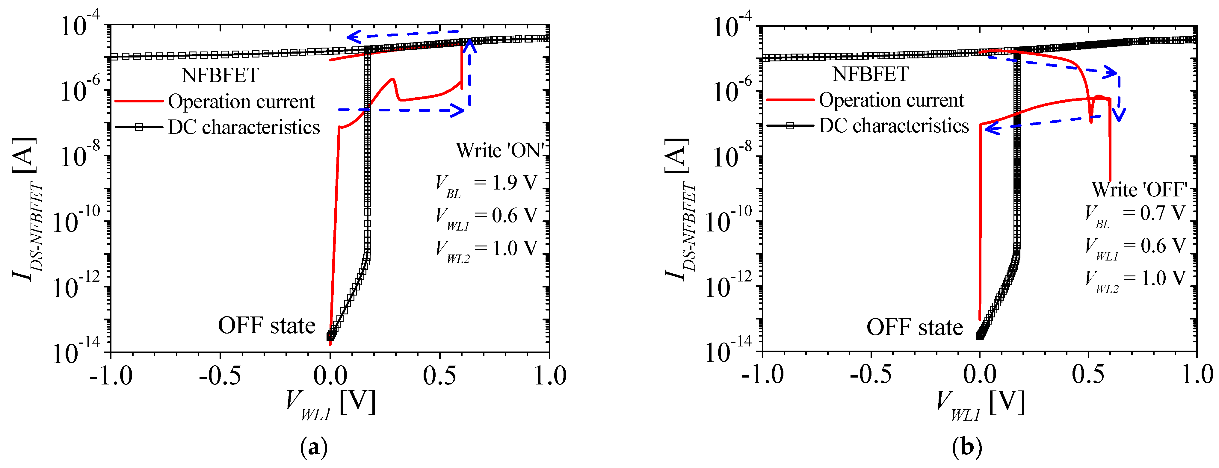
Figure 5.
Timing diagram of the M3D−FBFET−SRAM cell operation.
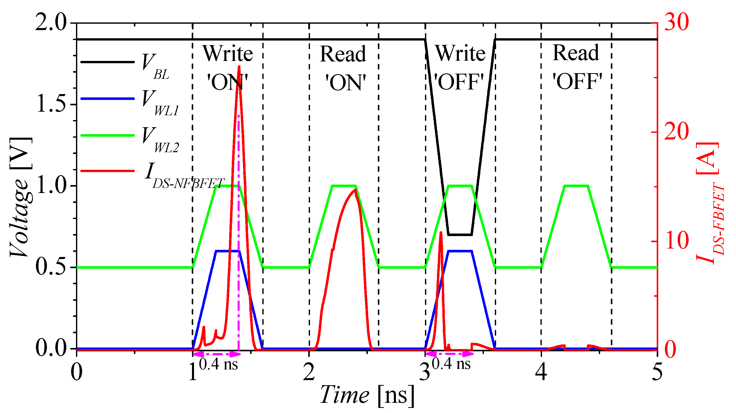
Figure 6.
Retention characteristics of the M3D−FBFET−SRAM cell when the recursive reading pulse is applied after (a) writing ‘ON’ operation, and (b) writing ‘OFF’ operation.
Figure 6.
Retention characteristics of the M3D−FBFET−SRAM cell when the recursive reading pulse is applied after (a) writing ‘ON’ operation, and (b) writing ‘OFF’ operation.
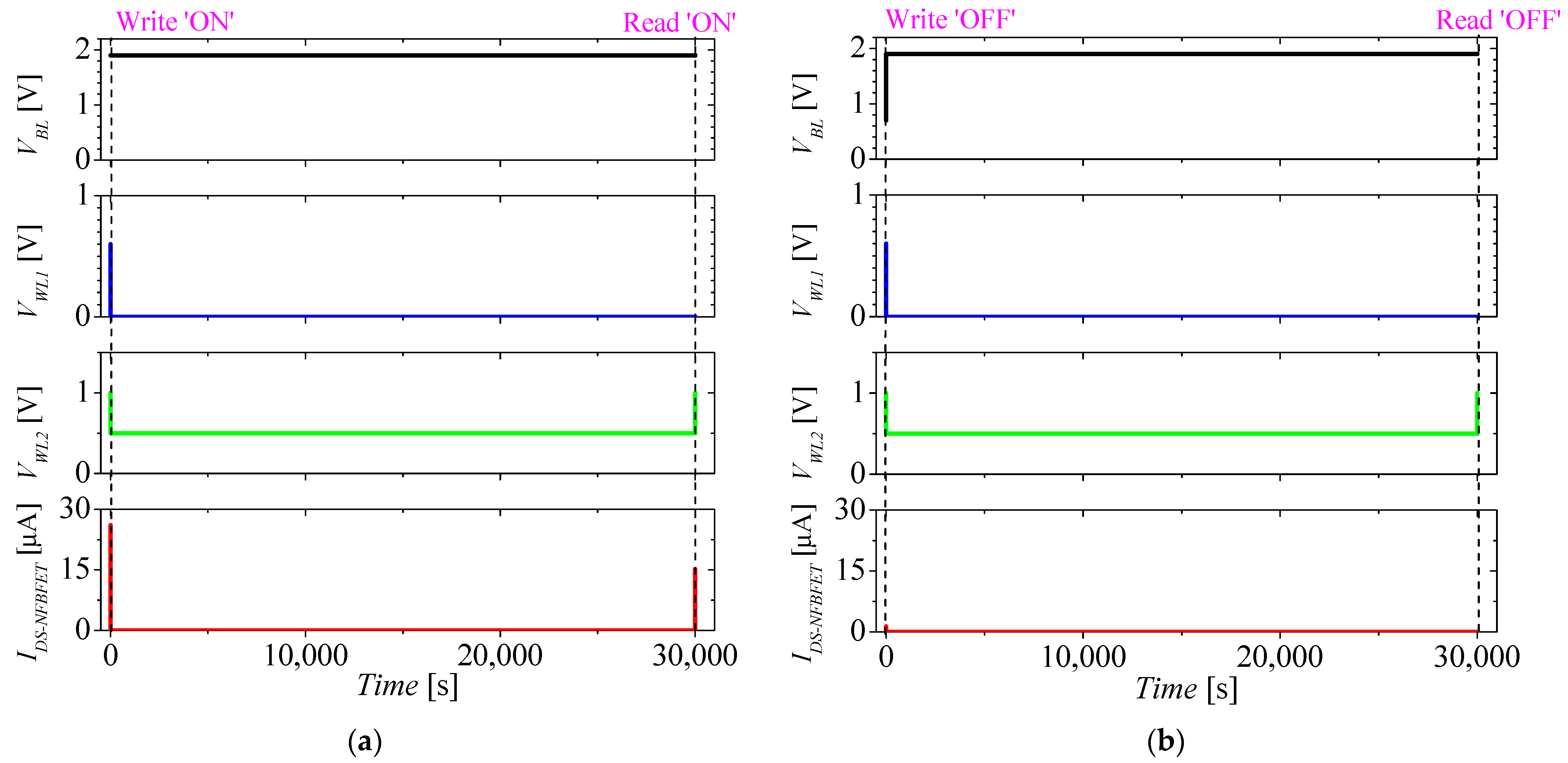
Figure 7.
(a) Changing threshold voltage at two different bottom transistor gate voltages (VWL1 = 0 and 0.6 V) at TILD = 3 nm. (b) The M3D−FBFET−SRAM cell operation with respect to various TILD.
Figure 7.
(a) Changing threshold voltage at two different bottom transistor gate voltages (VWL1 = 0 and 0.6 V) at TILD = 3 nm. (b) The M3D−FBFET−SRAM cell operation with respect to various TILD.

Figure 8.
The reading ‘ON’ current of the M3D−FBFET−SRAM cell with TILD = 3 nm. (a) VBL = 1.9 (black lines), and 2.2 V (red lines), and (b) VWL2 = 1.0 (black lines) to 1.2 V (red lines).
Figure 8.
The reading ‘ON’ current of the M3D−FBFET−SRAM cell with TILD = 3 nm. (a) VBL = 1.9 (black lines), and 2.2 V (red lines), and (b) VWL2 = 1.0 (black lines) to 1.2 V (red lines).


Table 1.
Structure parameters of the M3D-FBFET-SRAM cell.
| Parameters | Description | Value/Unit |
|---|---|---|
| Lungated | Length of the ungated channel region for the NFBFET | 40 nm |
| Lgated, Lchannel | Length of the gated channel region for the NFBFET and NMOSFET | 40 nm |
| LLDD | Length of the lightly doped drain (LDD) region | 10 nm |
| Tgate | Thickness of the gate | 30 nm |
| Tspacer | Thickness of the spacer | 33 nm |
| Toxide | Thickness of the gate oxide | 3 nm |
| Tsi | Thickness of the silicon body | 6 nm |
| TILD | Thickness of the interlayer dielectric (ILD) | Var. |
| Nsource, Ndrain | Doping concentration of the source and drain regions | 1 × 1020 cm−3 |
| Ngated | Doping concentration of the gated channel region for NFBFET | 2 × 1017 cm−3 |
| Nungated | Doping concentration of the ungated channel region for NFBFET | 1 × 1020 cm−3 |
| Nch | Doping concentration of the channel region for NMOSFET | 1 × 1015 cm−3 |
| NLDD | Doping concentration of the LDD region for NMOSFET | 1 × 1018 cm−3 |
Table 2.
The M3D−FBFET−SRAM cell operation voltages.
| Voltages | Write ‘ON’ | Write ‘OFF’ | Hold | Read |
|---|---|---|---|---|
| VBL | 1.9 V | 0.7 V | 1.9 V | 1.9 V |
| VWL1 | 0.6 V | 0.6 V | 0.0 V | 0.0 V |
| VWL2 | 1.0 V | 1.0 V | 0.5 V | 1.0 V |
Publisher’s Note: MDPI stays neutral with regard to jurisdictional claims in published maps and institutional affiliations. |
© 2022 by the authors. Licensee MDPI, Basel, Switzerland. This article is an open access article distributed under the terms and conditions of the Creative Commons Attribution (CC BY) license (https://creativecommons.org/licenses/by/4.0/).
Share and Cite
MDPI and ACS Style
Oh, J.H.; Yu, Y.S. A Monolithic 3-Dimensional Static Random Access Memory Containing a Feedback Field Effect Transistor. Micromachines 2022, 13, 1625. https://doi.org/10.3390/mi13101625
AMA Style
Oh JH, Yu YS. A Monolithic 3-Dimensional Static Random Access Memory Containing a Feedback Field Effect Transistor. Micromachines. 2022; 13(10):1625. https://doi.org/10.3390/mi13101625
Chicago/Turabian StyleOh, Jong Hyeok, and Yun Seop Yu. 2022. "A Monolithic 3-Dimensional Static Random Access Memory Containing a Feedback Field Effect Transistor" Micromachines 13, no. 10: 1625. https://doi.org/10.3390/mi13101625
Note that from the first issue of 2016, this journal uses article numbers instead of page numbers. See further details here.