Sputtered Modified Barium Titanate for Thin-Film Capacitor Applications

Abstract
:1. Introduction
2. Experimental Section
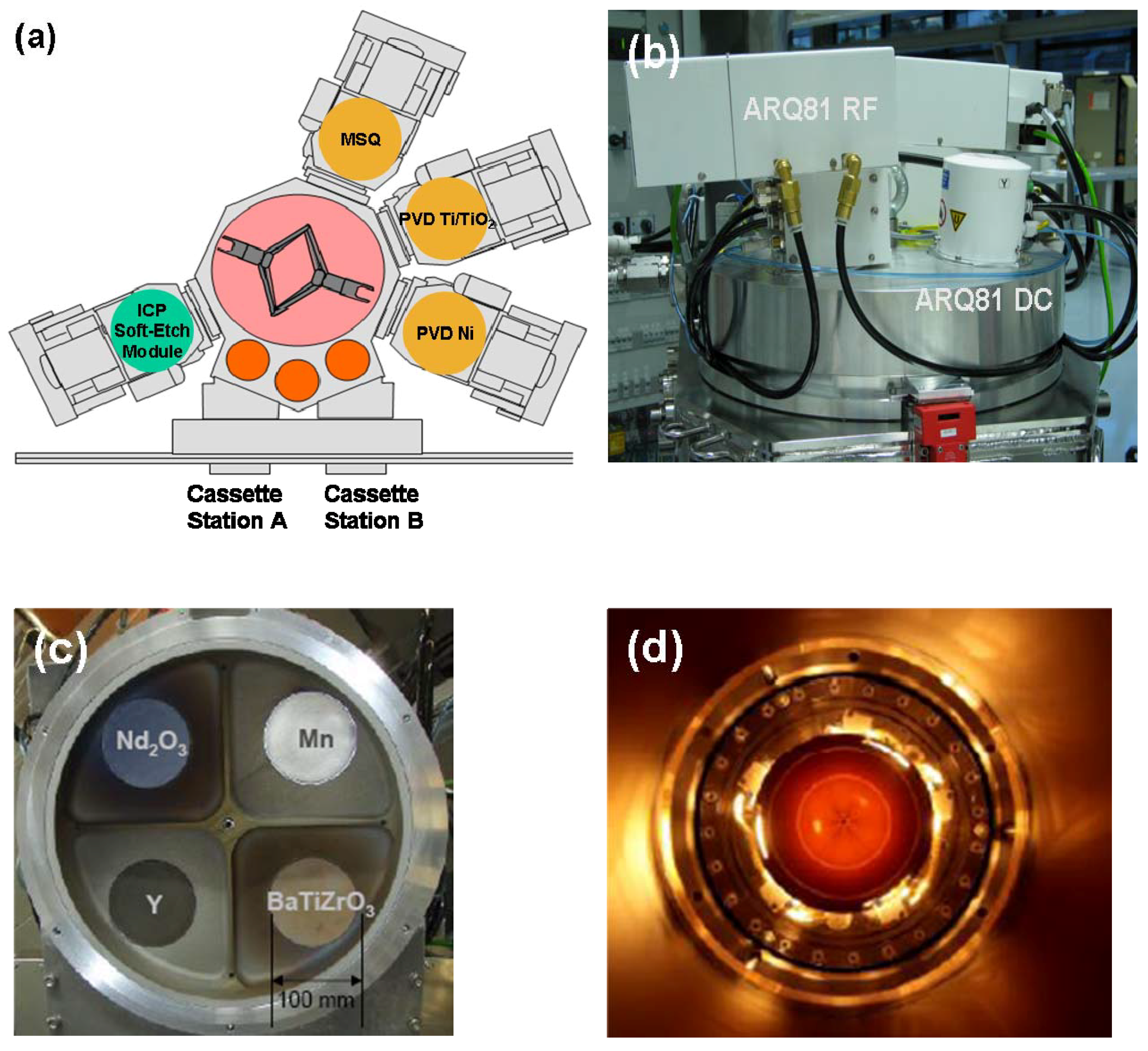
2.1. Apparatus
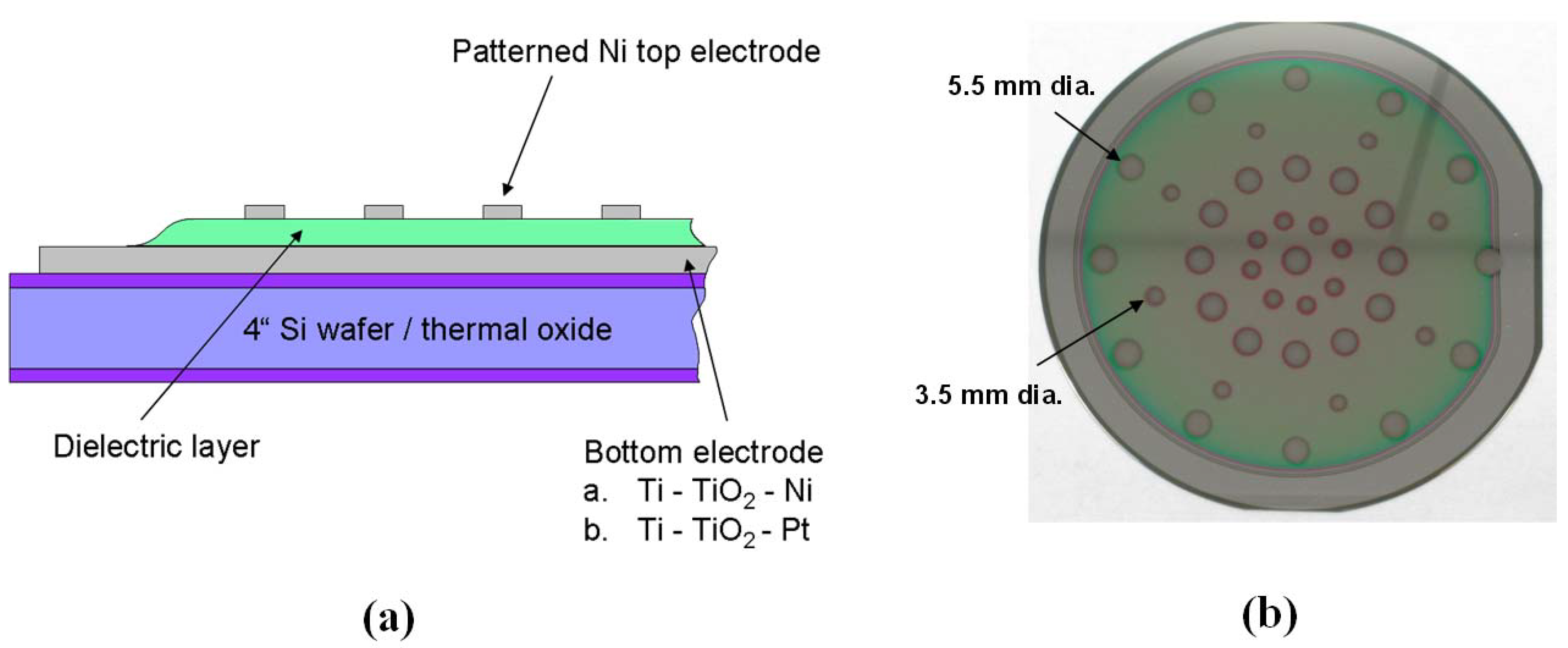
2.2. Deposition


| Deposition temperature (°C) | Target power (W) | Sputter pressure (mtorr) | % O2 in Ar | Rate (nm/s) |
|---|---|---|---|---|
| 700 | 250 | 4.5 | 0 | 0.0458 |
| 700 | 250 | 10.0 | 0 | 0.0394 |
| 700 | 250 | 4.5 | 10 | 0.0184 |
| 700 | 250 | 10.0 | 10 | 0.0163 |
| 700 | 250 | 4.5 | 15 | 0.0169 |
| 700 | 250 | 10.0 | 15 | 0.0145 |
| 800 | 250 | 7.25 | 5 | 0.0174 |
| 900 | 250 | 4.5 | 0 | 0.0454 |
| 900 | 250 | 10.0 | 0 | 0.0420 |
| 900 | 250 | 4.5 | 10 | 0.0185 |
| 900 | 250 | 10.0 | 10 | 0.0156 |
| 900 | 250 | 4.5 | 15 | 0.0168 |
| 900 | 250 | 10.0 | 15 | 0.0132 |

2.3. Characterization
3. Results and Discussion
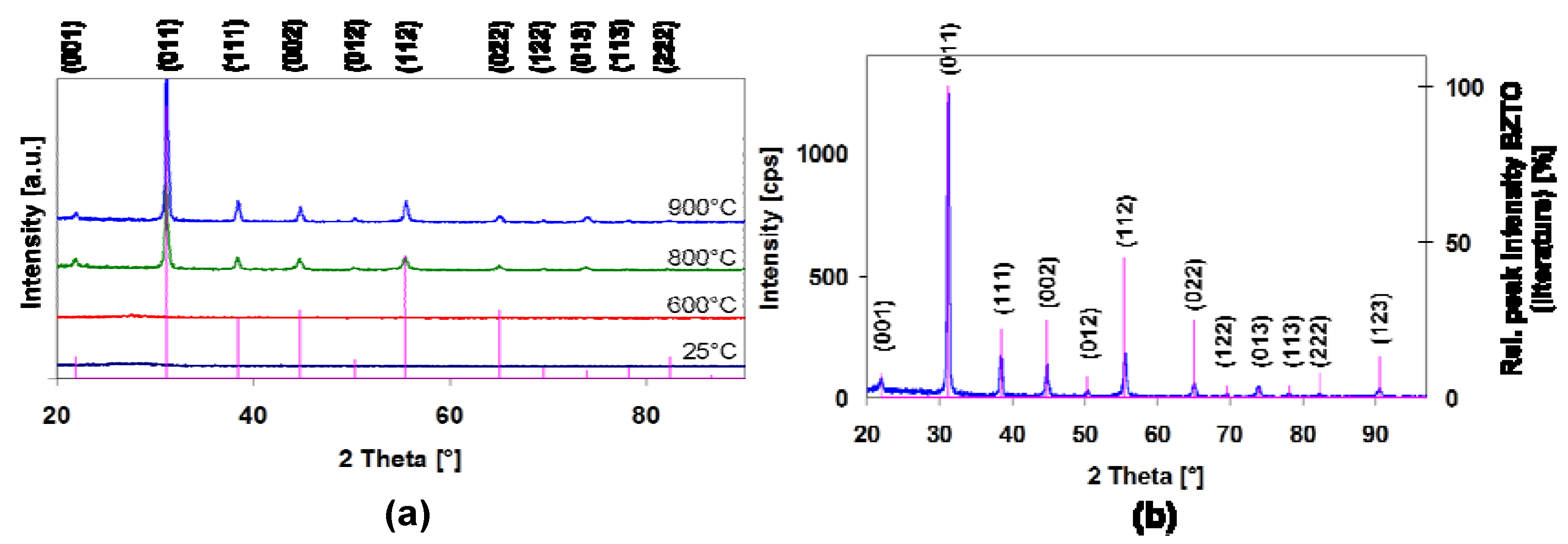
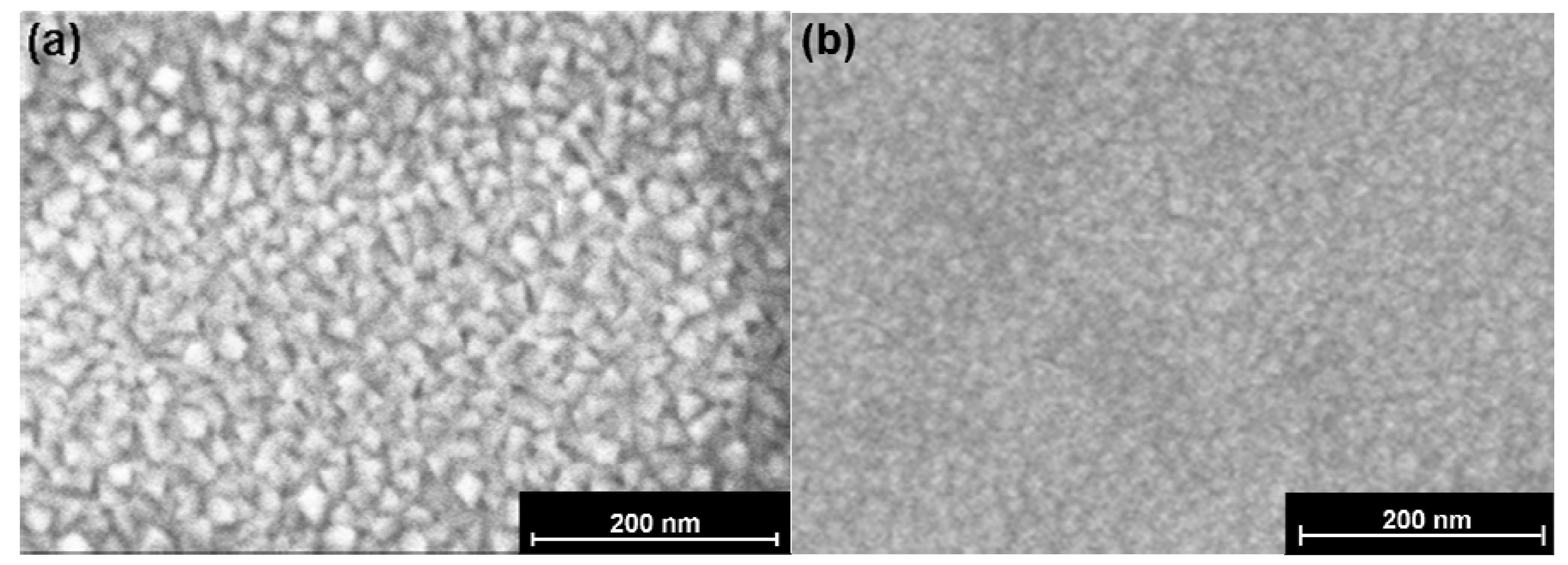
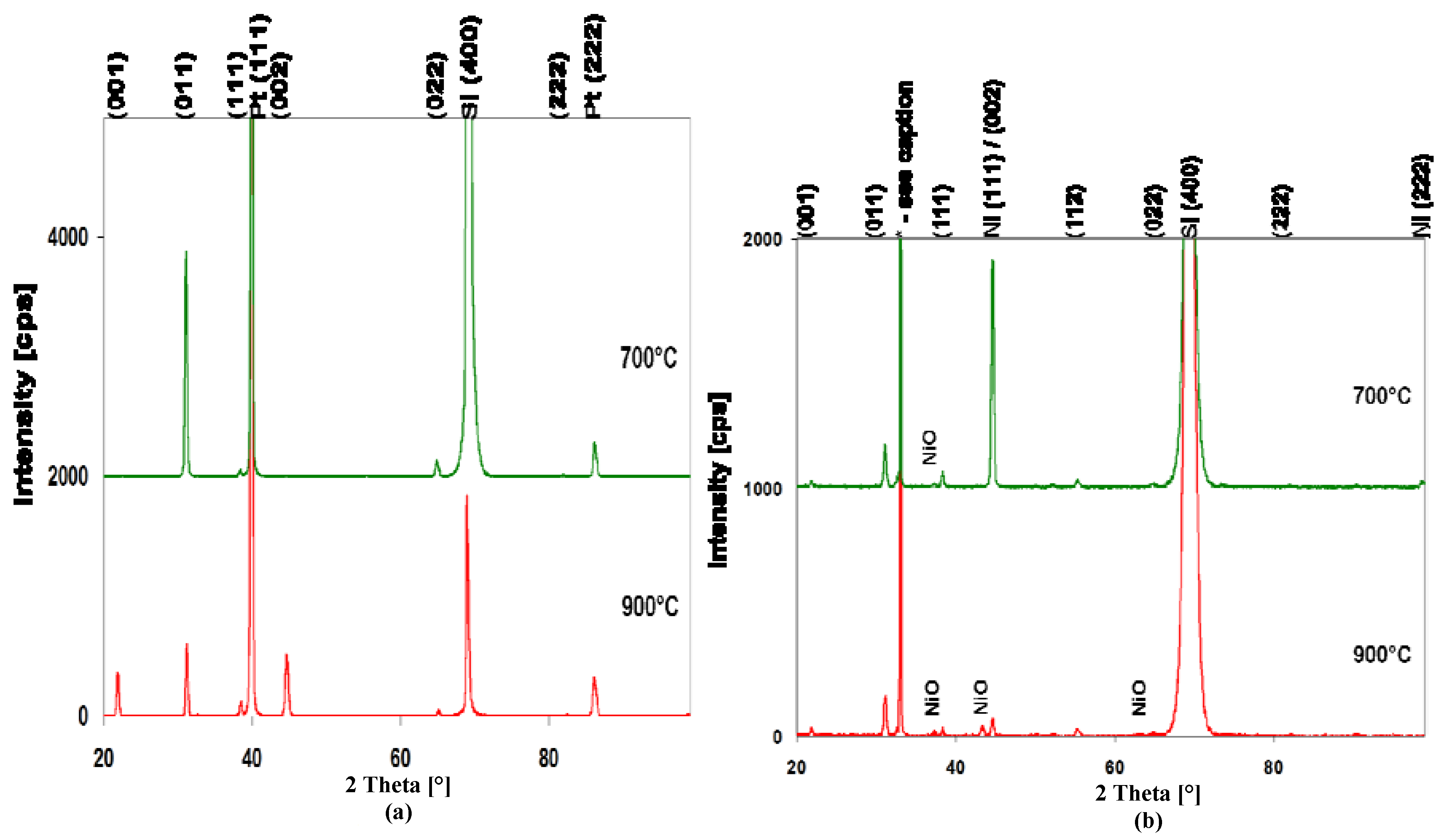
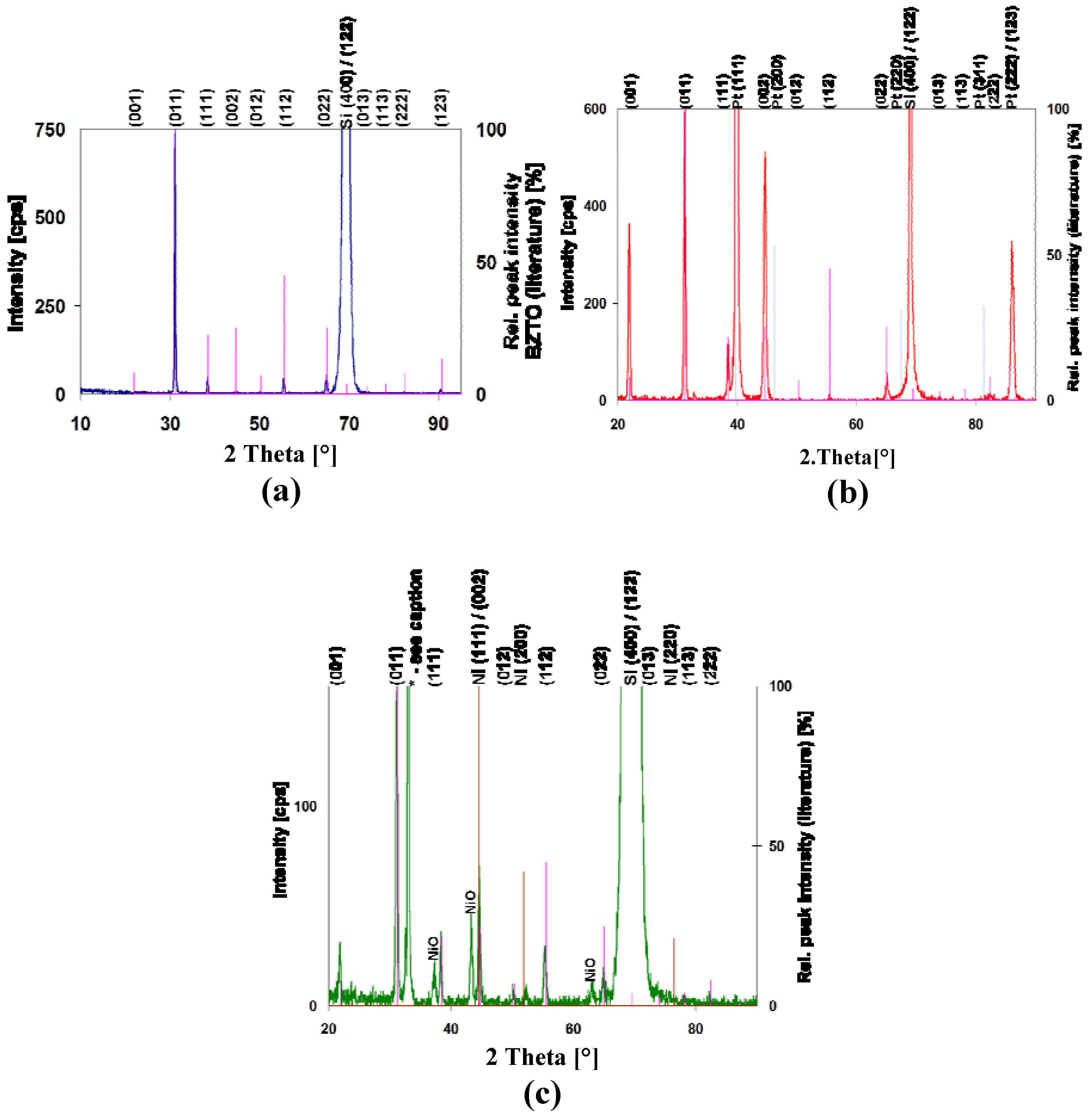
3.1. XRD and SEM


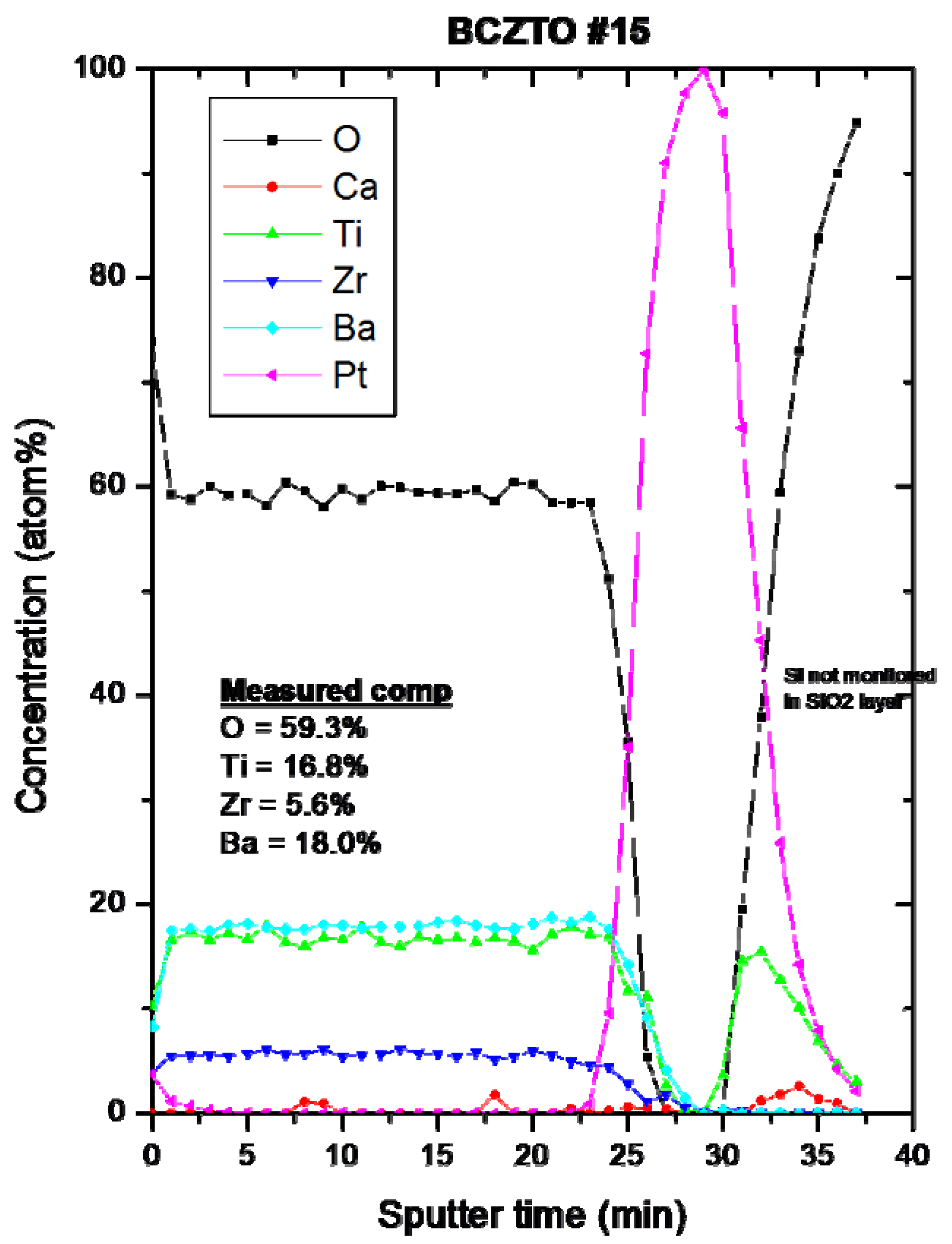
3.2. XPS
3.3. Electrical Characterization

| Bottom electrode | Top electrode | Dielectric Tdep (°C) | Process pressure (mtorr) | % O2 in Ar | εr | ρ (Ω∙cm) | Loss factor |
|---|---|---|---|---|---|---|---|
| Pt | Pt | 700 | 4.5 | 0 | 6.1 E+03 | ||
| 700 | 10 | 0 | 2.0 E+04 | ||||
| 700 | 4.5 | 10 | 633 | 2.7 E+09 | |||
| 700 | 10 | 10 | 596 | 2.4 E+09 | |||
| 800 | 7.25 | 5 | 1006 | 2.8 E+09 | |||
| 900 | 4.5 | 0 | 2.2 E+05 | ||||
| 900 | 10 | 0 | 899 | 4.0 E+09 | |||
| 900 | 4.5 | 10 | 1213 | 2.3 E+09 | |||
| 900 | 10 | 10 | 1023 | 4.1 E+09 | |||
| Pt | Ni | 700 | 4.5 | 0 | 2018 | 1.2 E+08 | 0.66 |
| 700 | 10 | 0 | 845 | 5.5 E+08 | 0.14 | ||
| 700 | 4.5 | 10 | 900 | 5.3 E+08 | 0.13 | ||
| 700 | 10 | 10 | 867 | 2.5 E+08 | 0.23 | ||
| 700 | 4.5 | 15 | 659 | 1.5 E+09 | |||
| 700 | 10 | 15 | 529 | 1.3 E+09 | |||
| 800 | 7.25 | 5 | 1149 | 5.6 E+08 | 0.17 | ||
| 900 | 4.5 | 0 | 2.0 E+04 | ||||
| 900 | 10 | 0 | 1280 | 2.0 E+09 | 0.03 | ||
| 900 | 4.5 | 10 | 1359 | 2.0 E+09 | 0.03 | ||
| 900 | 10 | 10 | 1327 | 2.5 E+09 | 0.017 | ||
| 900 | 4.5 | 15 | 1212 | 3.2 E+09 | |||
| 900 | 10 | 15 | 1193 | 3.4 E+09 | |||
| Ni | Ni | 700 | 4.5 | 0 | 1738 | 3.6 E+08 | |
| 700 | 10 | 0 | 964 | 1.8 E+08 | |||
| 700 | 4.5 | 10 | 331 | 3.9 E+09 | |||
| 700 | 10 | 10 | 398 | 8.0 E+08 | |||
| 800 | 7.25 | 5 | 123 | 4.6 E+08 | |||
| 900 | 4.5 | 0 | 3.9 E+04 | ||||
| 900 | 10 | 0 | 1664 | 3.2 E+08 | |||
| 900 | 4.5 | 10 | 100 | 1.8 E+09 | |||
| 900 | 10 | 10 | 144 | 3.3 E+08 |
| Bottom electrode | Top electrode | Dielectric Tdep (°C) | Process pressure (mtorr) | % O2 in Ar | εr | ρ (Ω∙cm) | Dep. rate vs. reference | |
|---|---|---|---|---|---|---|---|---|
| Pt | Ni | Layer 1 | 900 | 4.5 | 10 | 1091 | 3.4 E+08 | +42% |
| Layer 2 | 900 | 4.5 | 0 | |||||
| Layer 1 | 900 | 4.5 | 10 | 1131 | 2.5 E+09 | +35% | ||
| Layer 2 | 900 | 10 | 0 | |||||
| Layer 1 | 900 | 4.5 | 10 | 1261 | 2.7 E+09 | -9% | ||
| Layer 2 | 900 | 10 | 10 | |||||
| Reference | 900 | 4.5 | 10 | 1359 | 2.0 E+09 | – |
3.4. Discussion
4. Conclusions
Acknowledgments
References
- Bhalla, A.S.; Guo, R.; Roy, R. The perovskite structure—A review of its role in ceramic science and technology. Mat. Res. Innovat. 2000, 4, 3–26. [Google Scholar] [CrossRef]
- Hansen, P. Multilayer capacitor comprising barium-titanate doped with silver and rare earth metal. U.S. Patent 6,078,494, 20 June 2000. [Google Scholar]
- Kishi, H.; Mizuno, Y.; Chazono, H. Base-metal electrode-multilayer ceramic capacitors: past, present and future perspectives. Jpn. J. Appl. Phys. 2003, 42, 1–15. [Google Scholar] [CrossRef]
- Weir, R.D.; Nelson, C.W. Electrical-energy-storage unit (EESU) utilizing ceramic and integrated-circuit technologies for replacement of electrochemical batteries. U.S. Patent 7,033,406, 25 April 2006. [Google Scholar]
- Weir, R.D.; Nelson, C.W. Utilization of poly(ethylene terephthalate) plastic and composition-modified barium titanate powders in a matrix that allows polarization and the use of integrated-circuit technologies for the production of lightweight ultrahigh electrical energy storage units (EESU). U.S. Patent 7,466,536, 16 December 2008. [Google Scholar]
- Weir, R.D.; Nelson, C.W. Electrical-energy-storage unit (EESU) utilizing ceramic and integrated-circuit technologies for replacement of electrochemical batteries. US Patent 7,595,109, 29 September 2009. [Google Scholar]
- Yoon, D.-H.; Lee, B.I. Processing of barium titanate tapes with different binders for MLCC applications—Part I: Optimization using design of experiments. J. Eur. Ceram. Soc. 2004, 24, 739–752. [Google Scholar] [CrossRef]
- Randall, M.; Skamser, D.; Kinard, T.; Qazi, J.; Tajuddin, A.; Trolier-McKinstry, S.; Randall, C.; Ko, S.W.; Dechakupt, T. Thin Film MLCC. In CARTS USA 2007 Symposium Proceedings; Electronic Components, Assemblies & Materials Association (ECA), Arlington, VA, USA: Albuquerque, NM, USA, 2007; pp. 403–415. [Google Scholar]
- Bhattacharya, S.K.; Tummala, R.R. Integral passives for next generation of electronic packaging: Application of epoxy/ceramic nanocomposites as integral capacitors. Microelect. J. 2001, 32, 11–19. [Google Scholar] [CrossRef]
- Jain, P.; Rymaszewski, E.J. Thin-Film Capacitors for Packaged Electronics; Kluwer Academic Publishers: Norwell, MA, USA, 2004. [Google Scholar]
- Wojnowski, M.; Pressel, K.; Sommer, G.; Engl, M. Package trends for today’s and future mm-wave applications. In Presented at EuMIC 2008, 38th European Microwave Conference, Amsterdam, The Netherlands, 27–28 October 2008.
- Sakka, S.; Kamiya, K.; Makita, K.; Yamamoto, Y. Formation of sheets and coating films from alkoxide solutions. J. Non-Cryst. Solids 1984, 63, 223–235. [Google Scholar] [CrossRef]
- Mohallem, N.D.S.; Aegerter, M.A. Sol-gel processed BaTiO3. In Better Ceramics Through Chemistry III; Brinker, C.J., Clark, D.E., Ulrich, D.R., Eds.; MRS: Pittsburg, PA, USA, 1988; Volume 121, pp. 515–518. [Google Scholar]
- Bell, J.M.; Ben-Nissan, B.; Anast, M.; West, B.O.; Spiccia, L.; Cullen, J.; Watkins, I.; De Villiers, D.; Johnston, G. Sol-gel deposition of electronic ceramic films. In Better Ceramics through Chemistry IV; Zelinsky, B.J.J., Brinker, C.J., Clark, D.E., Ulrich, D.R., Eds.; MRS: Pittsburg, PA, USA, 1990; Volume 180, pp. 453–456. [Google Scholar]
- Anast, M.; Wong, A.; Bell, J.M.; Ben-Nissan, B.; Cullen, J.; Spiccia, L.; De Villiers, D.; Watkins, I.; West, B.O.; Johnston, G. Thin film ceramic coatings via the sol-gel process. Key Eng. Mat. 1991, 53–55, 427–432. [Google Scholar] [CrossRef]
- Bahtat, A.; Mugnier, J.; Bahtat, M.; Bovier, C.; Serughetti, J. Sol-gel processed barium titanate waveguides. J. Sol-Gel Sci. Technol. 1994, 2, 555–558. [Google Scholar] [CrossRef]
- Feil, W.A.; Wessels, B.W.; Tonge, L.M.; Marks, T.J. Organometallic chemical vapor deposition of strontium titanate. J. Appl. Phys. 1990, 67, 3858–3861. [Google Scholar] [CrossRef]
- Kawahara, T.; Yamauka, M.; Makita, T.; Naka, J.; Yuuki, A.; Mikami, N.; Ono, K. Step coverage and electrical properties of (Ba, Sr)TiO3 films prepared by liquid source chemical vapor deposition using TiO(DPM)2. Jpn. J. Appl. Phys. 1994, 33, 5129–5134. [Google Scholar] [CrossRef]
- Sakabe, Y.; Takeshima, Y.; Tanaka, K. Multilayer ceramic capacitors with thin (Ba,Sr)TiO3 layers by MOCVD. J. Electroceram. 1999, 3, 115–121. [Google Scholar] [CrossRef]
- Weiss, F.; Lindner, J.; Sénateur, J.P.; Dubourdieu, C.; Galindo, V.; Audier, M.; Abrutis, A.; Rosina, M.; Fröhlich, K.; Haessler, W.; et al. Injection MOCVD: ferroelectric thin films and functional oxide superlattices. Surf. Coat. Technol. 2000, 133–134, 191–197. [Google Scholar] [CrossRef]
- Kuwata, J.; Fujita, Y.; Matsuoka, T.; Tohda, T.; Nishikawa, M.; Abe, A. Electrical properties of perovskite type oxide thin-films prepared by RF sputtering. Jpn. J. Appl. Phys. 1985, 24, 413–415. [Google Scholar] [CrossRef]
- Jia, Q.X.; Chang, L.H.; Anderson, W.A. Low leakage current BaTiO3 thin film capacitors using a multilayer construction. Thin Solid Films 1995, 259, 264–269. [Google Scholar] [CrossRef]
- Wu, T.B.; Wu, C.M.; Chen, M.L. Highly insulative barium zirconate-titanate thin films prepared by RF magnetron sputtering for dynamic random access memory applications. Appl. Phys. Lett. 1996, 69, 2659–2661. [Google Scholar] [CrossRef]
- Su, Q.X.; Rabson, T.A.; Robert, M.; Xiong, J.X.Z.; Moss, S.C. Growth of (211) BaTiO3 thin films on Pt-coated Si(100) substrates by radio frequency magnetron sputtering. Thin Solid Films 1997, 305, 227–231. [Google Scholar] [CrossRef]
- Vayunandana Reddy, Y.K.; Mergel, D.; Reuter, S.; Buck, V.; Sulkowski, M. Structural and optical properties of BaTiO3 thin films prepared by radio-frequency magnetron sputtering at various substrate temperatures. J. Phys. D Appl. Phys. 2006, 39, 1161–1168. [Google Scholar] [CrossRef]
- Sreenivas, K.; Reaney, I.; Maeder, T.; Setter, N.; Jagadish, C.; Elliman, R. Investigation of Pt/Ti bilayer metallization on silicon for ferroelectric thin film integration. J. Appl. Phys. 1994, 75, 232–239. [Google Scholar] [CrossRef]
- Hennings, D.; Schnell, A.; Simon, G. Diffuse ferroelectric phase transitions in Ba(Ti1−yZry)O3 ceramics. J. Am. Ceram. Soc. 1982, 65, 539–544. [Google Scholar] [CrossRef]
- Swanson, H.E.; Tatge, E. Standard X-ray Diffraction Powder Patterns; U.S. Dept. of Commerce, National Bureau of Standards: Washington, DC, USA, 1953; Volume 1, p. 31. [Google Scholar]
- Swanson, H.E.; Tatge, E. Standard X-ray Diffraction Powder Patterns; U.S. Dept. of Commerce, National Bureau of Standards: Washington, DC, USA, 1953; Volume 1, p. 13. [Google Scholar]
- Wies, S.; Eysel, W. JCPDS data of NiO (ICDD #44–1159), mineral.-petrograph., ICDD grant-in-Aid; Institut der Universitaet Heidelberg: Heidelberg, Germany, 1992. [Google Scholar]
- Herbert, J.M. Ceramic Dielectrics and Capacitors; Electrocomponent Science Monographs, Gordon and Breach Scientific Publishers: Philadelphia, PA, USA, 1985; Volume 6. [Google Scholar]
- Heywang, W. Semiconducting barium titanate. J. Mater. Sci. 1971, 6, 1214–1226. [Google Scholar] [CrossRef]
- Albertsen, K.; Hennings, D.; Steigelmann, O. Donor-acceptor charge complex formation in barium titanate ceramics: Role of firing atmosphere. J. Electroceram. 1998, 2, 193–198. [Google Scholar] [CrossRef]
- Reynolds, G.J.; Kratzer, M.; Dubs, M.; Felzer, H.; Mamazza, R. Electrical properties of thin-film capacitors fabricated using high temperature sputtered modified barium titanate. Materials 2012, in press. [Google Scholar]
© 2012 by the authors; licensee MDPI, Basel, Switzerland. This article is an open access article distributed under the terms and conditions of the Creative Commons Attribution license (http://creativecommons.org/licenses/by/3.0/).
Share and Cite
Reynolds, G.J.; Kratzer, M.; Dubs, M.; Felzer, H.; Mamazza, R. Sputtered Modified Barium Titanate for Thin-Film Capacitor Applications. Materials 2012, 5, 575-589. https://doi.org/10.3390/ma5040575
Reynolds GJ, Kratzer M, Dubs M, Felzer H, Mamazza R. Sputtered Modified Barium Titanate for Thin-Film Capacitor Applications. Materials. 2012; 5(4):575-589. https://doi.org/10.3390/ma5040575
Chicago/Turabian StyleReynolds, Glyn J., Martin Kratzer, Martin Dubs, Heinz Felzer, and Robert Mamazza. 2012. "Sputtered Modified Barium Titanate for Thin-Film Capacitor Applications" Materials 5, no. 4: 575-589. https://doi.org/10.3390/ma5040575