Porous Silicon—A Versatile Host Material

Abstract
:1. Introduction
1.1. Historical and general remarks on porous silicon
1.2. Functionalization of porous silicon
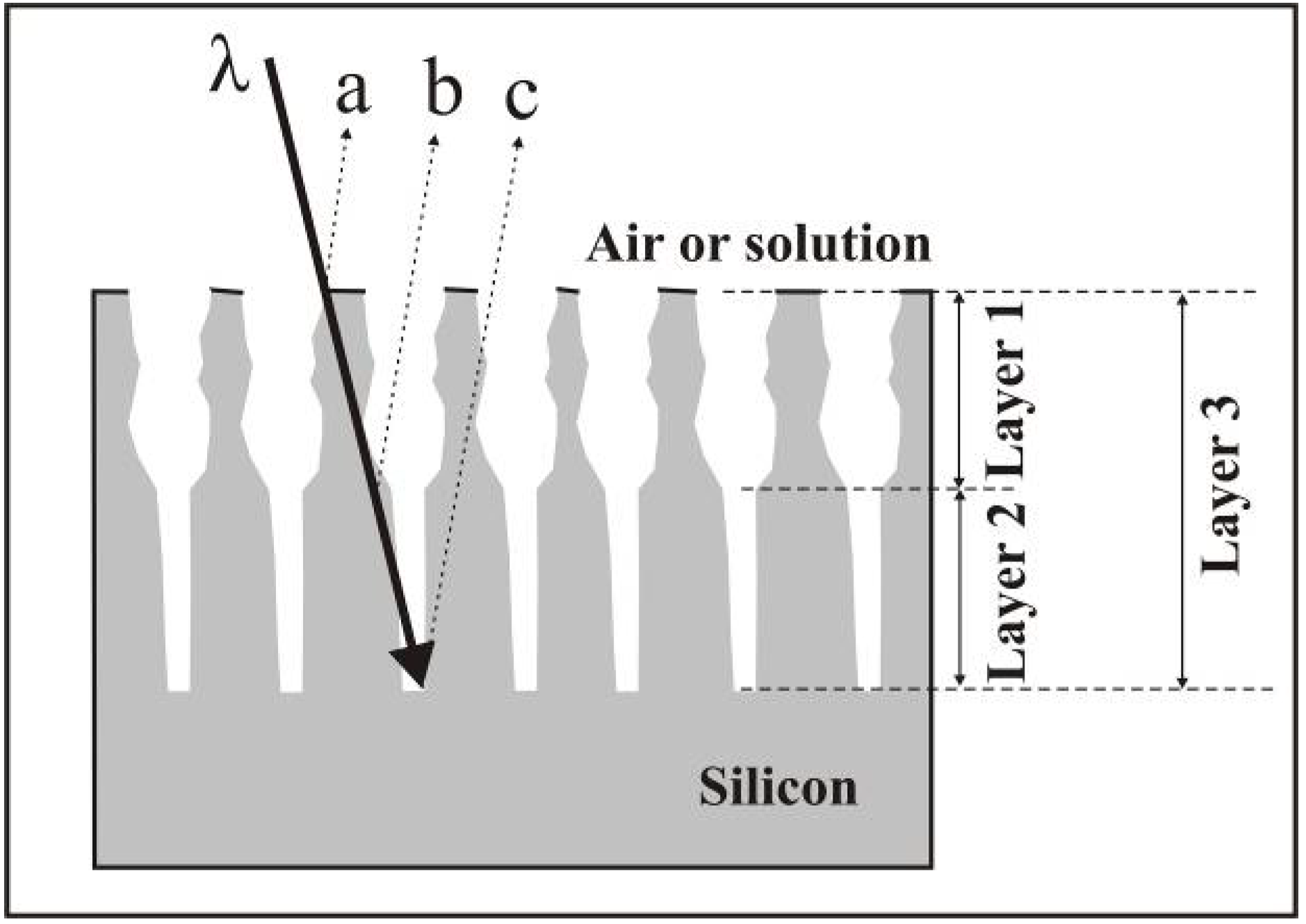
1.3. Applications of porous silicon


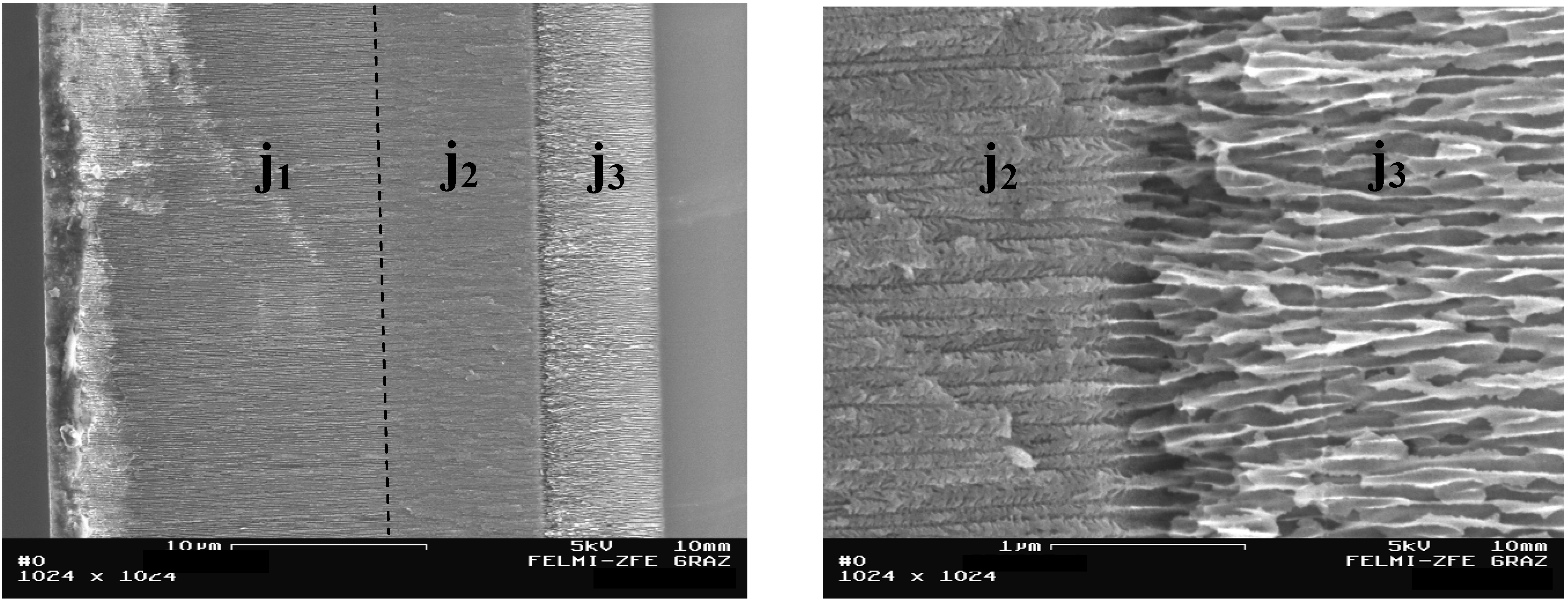
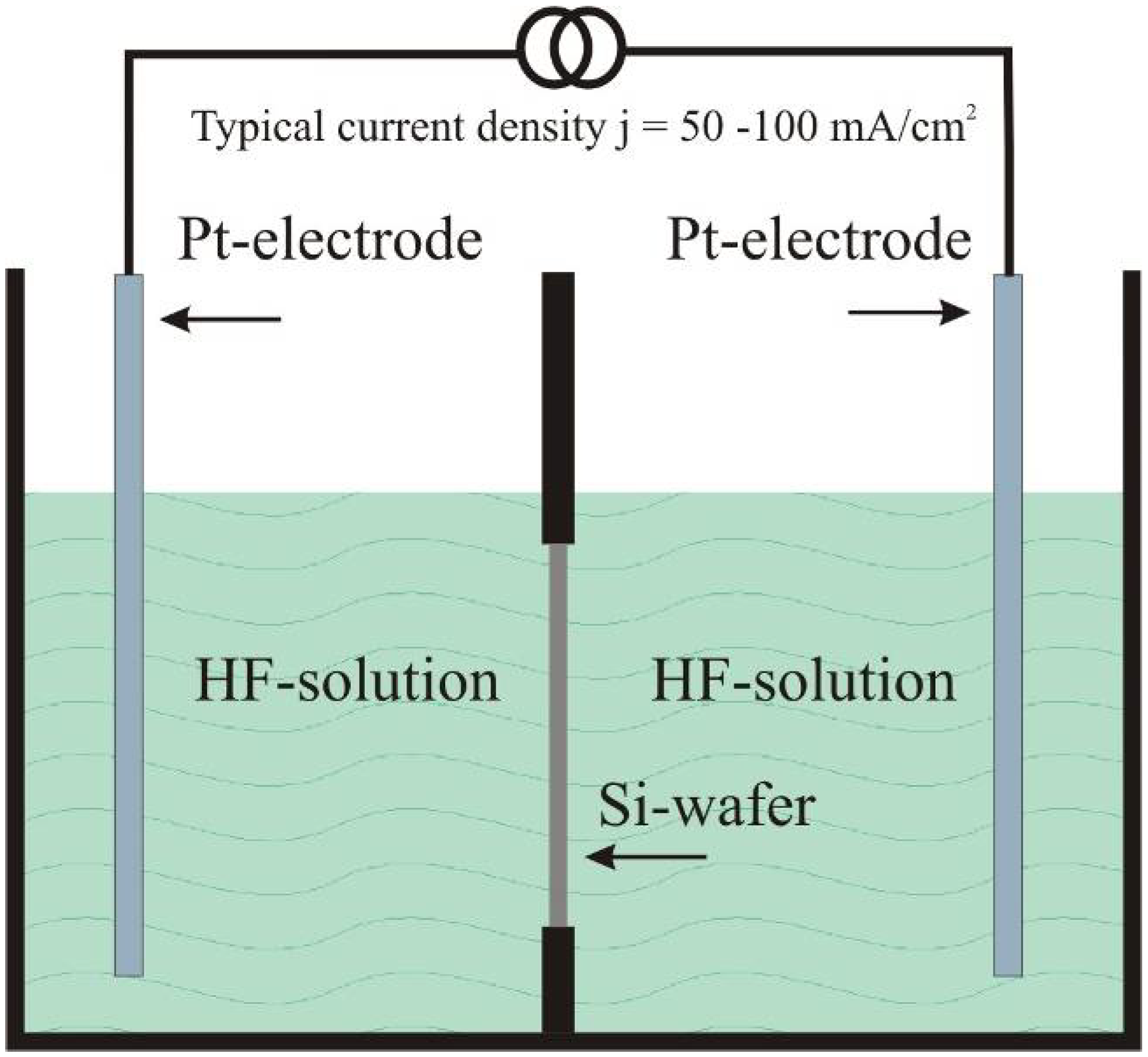
2. Fabrication of Porous Silicon by Anodic Dissolution of Bulk Crystalline Silicon

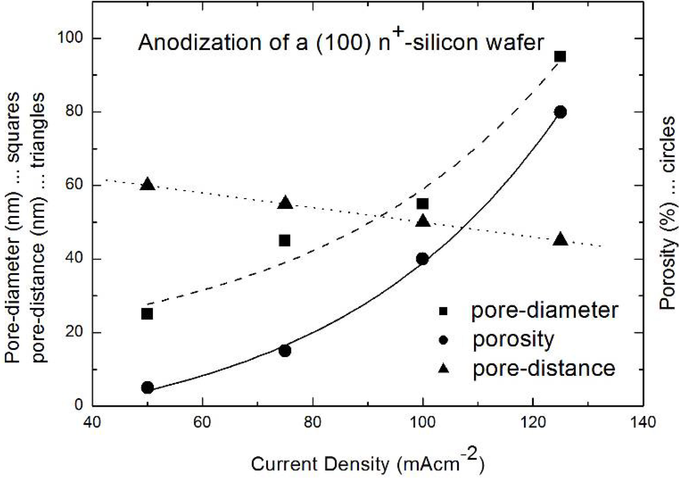
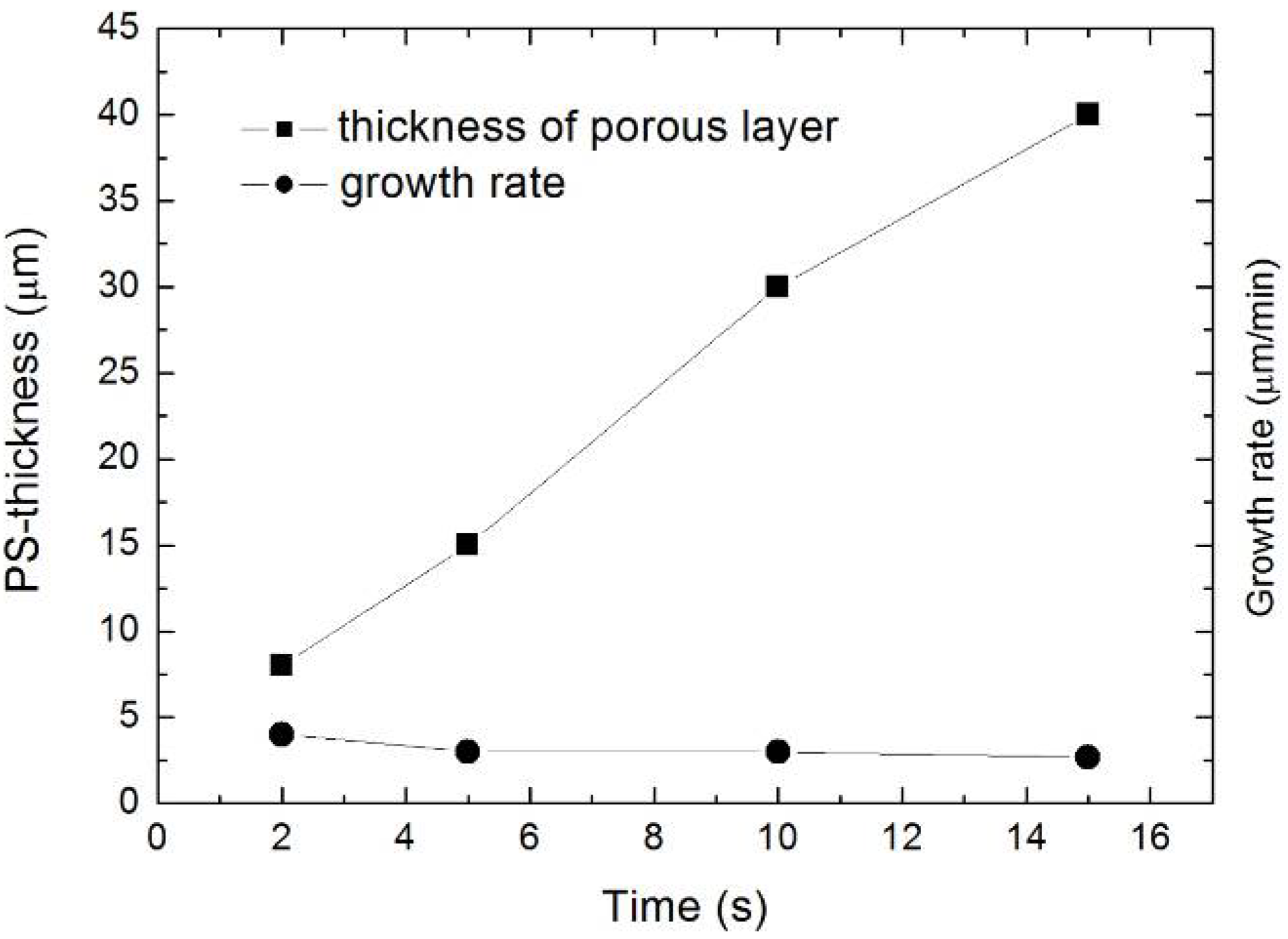
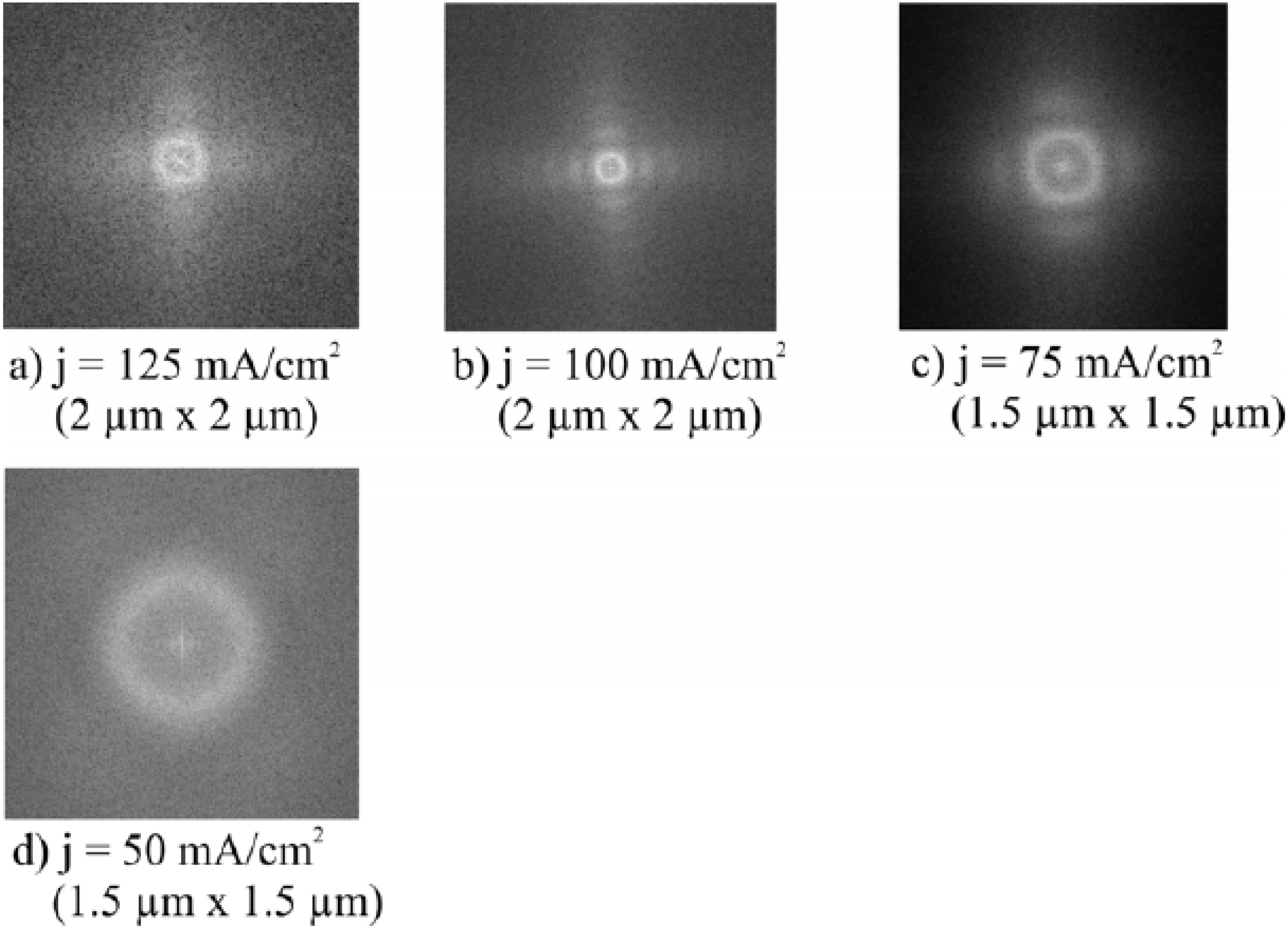
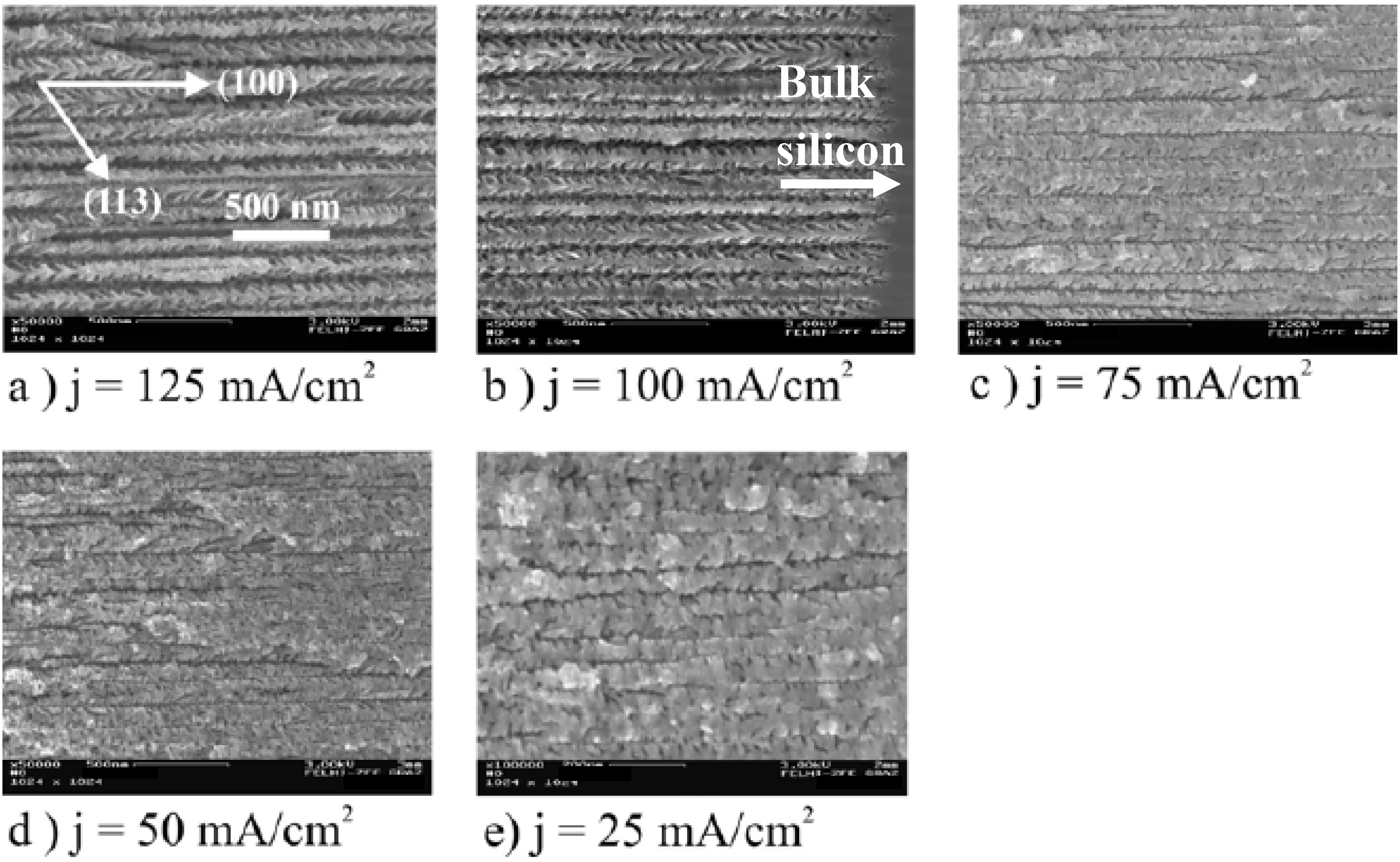
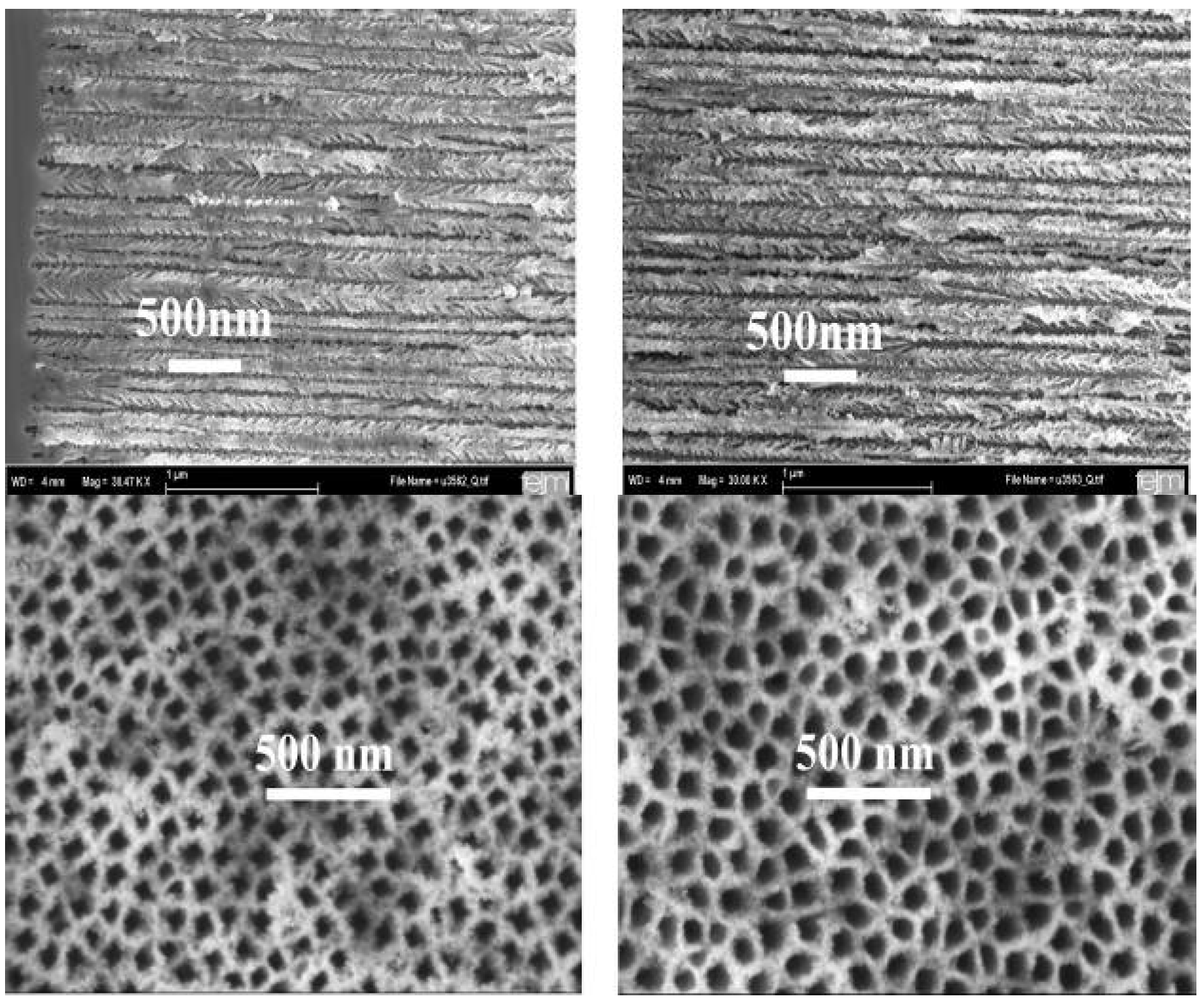
2.1. Self-organized pore growth
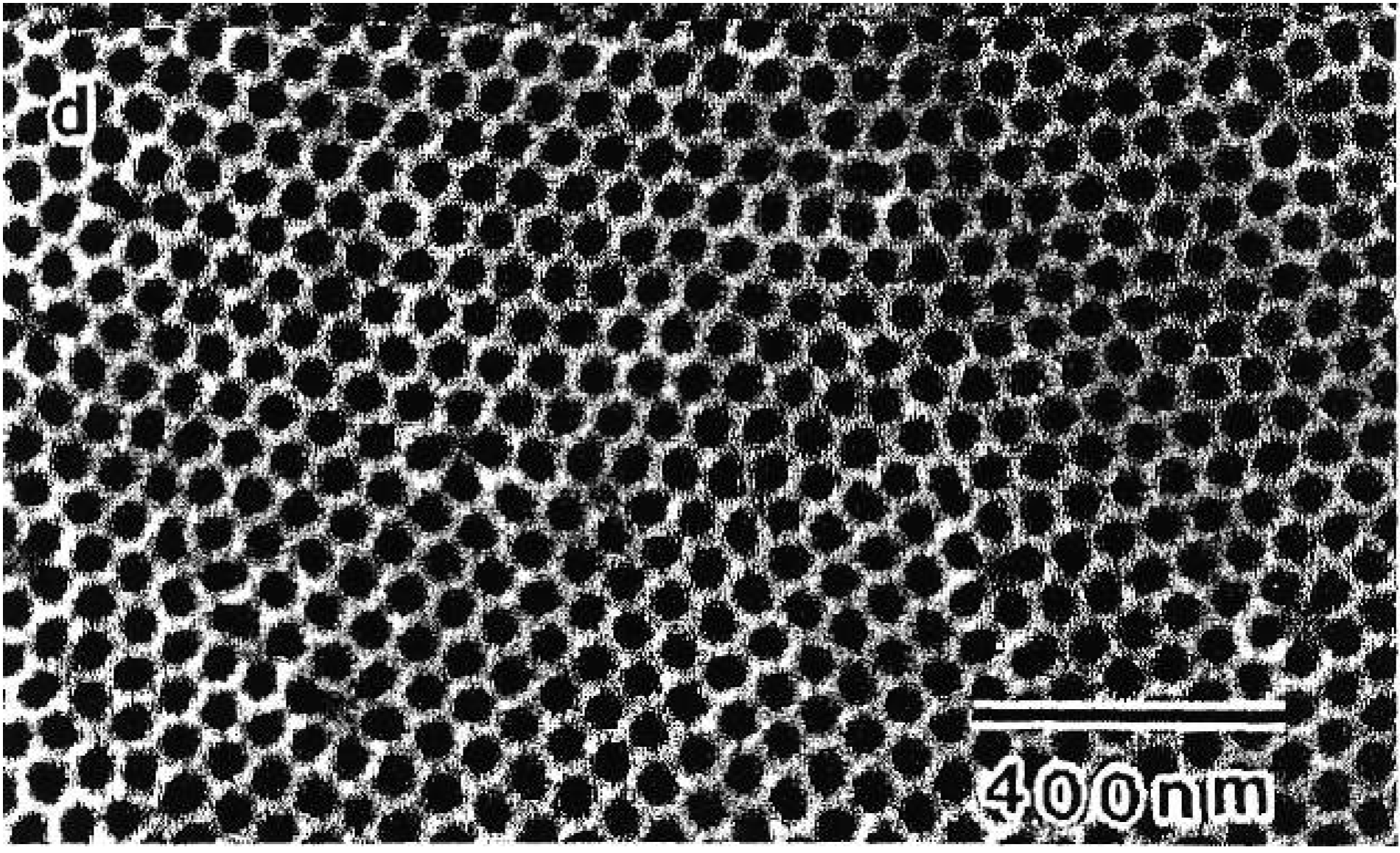
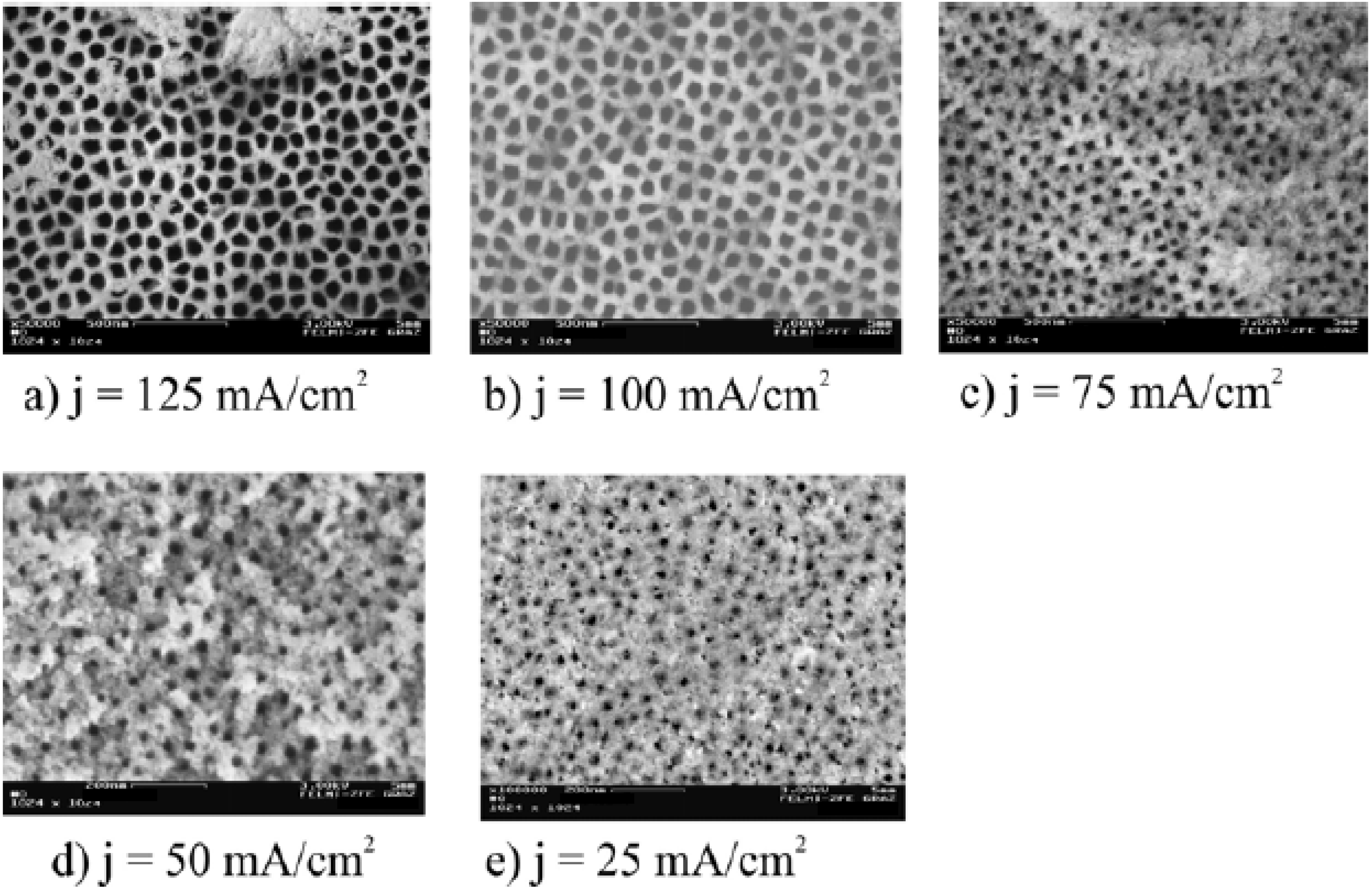
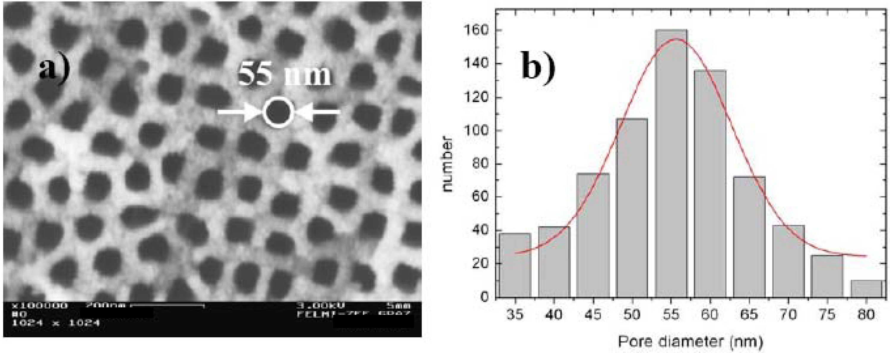
2.2. Fabrication of quasi-regular arranged mesopores

| Time (s) | PS-thickness (µm) | Growth rate (µm/min) |
|---|---|---|
| 2 | 8 | 4 |
| 5 | 15 | 3 |
| 10 | 30 | 3 |
| 15 | 40 | 2.7 |


2.3. Pore formation dependent on the crystal orientation

| Current density [mAcm-2] | Electrolyte concentration [wt%] | Pore-diameter [nm] | Pore-distance [nm] |
|---|---|---|---|
| 100 | 15 | 25 | 80 |
| 100 | 10 | 55 | 50 |
| 100 | 5 | Branched pores | - |
| 50 | 5 | 95 | 45 |
| 50 | 3 | 105 | 25 |
2.4. Further specific methods of pore formation
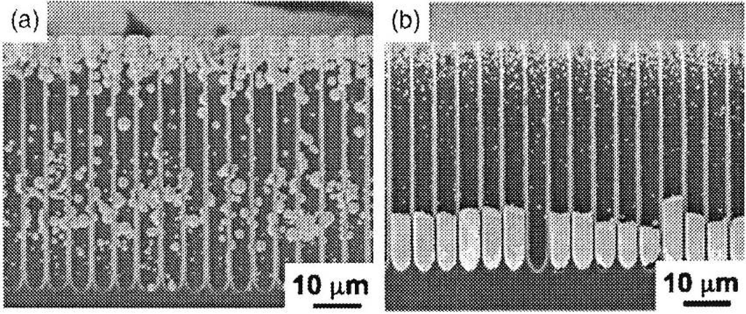
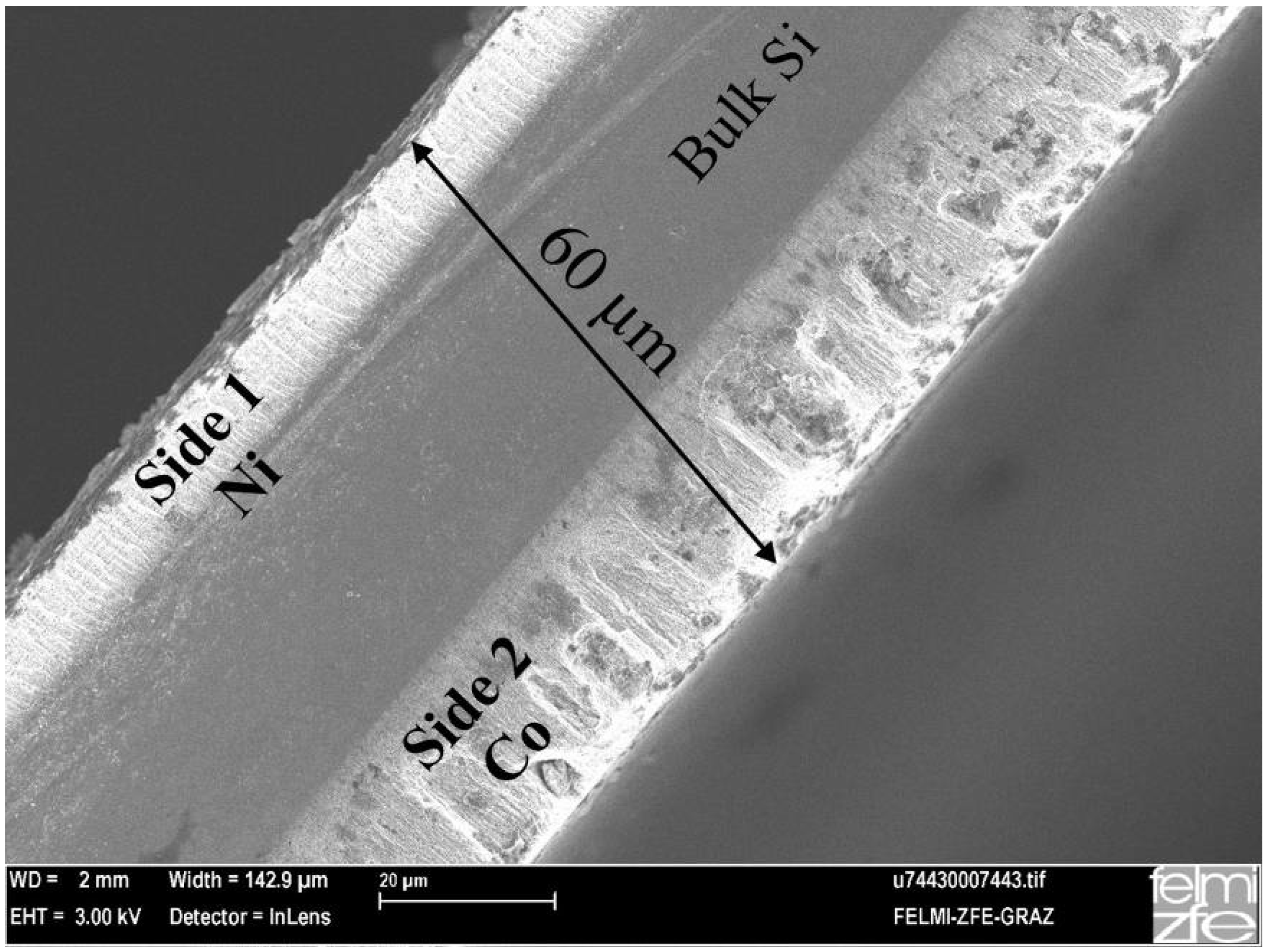
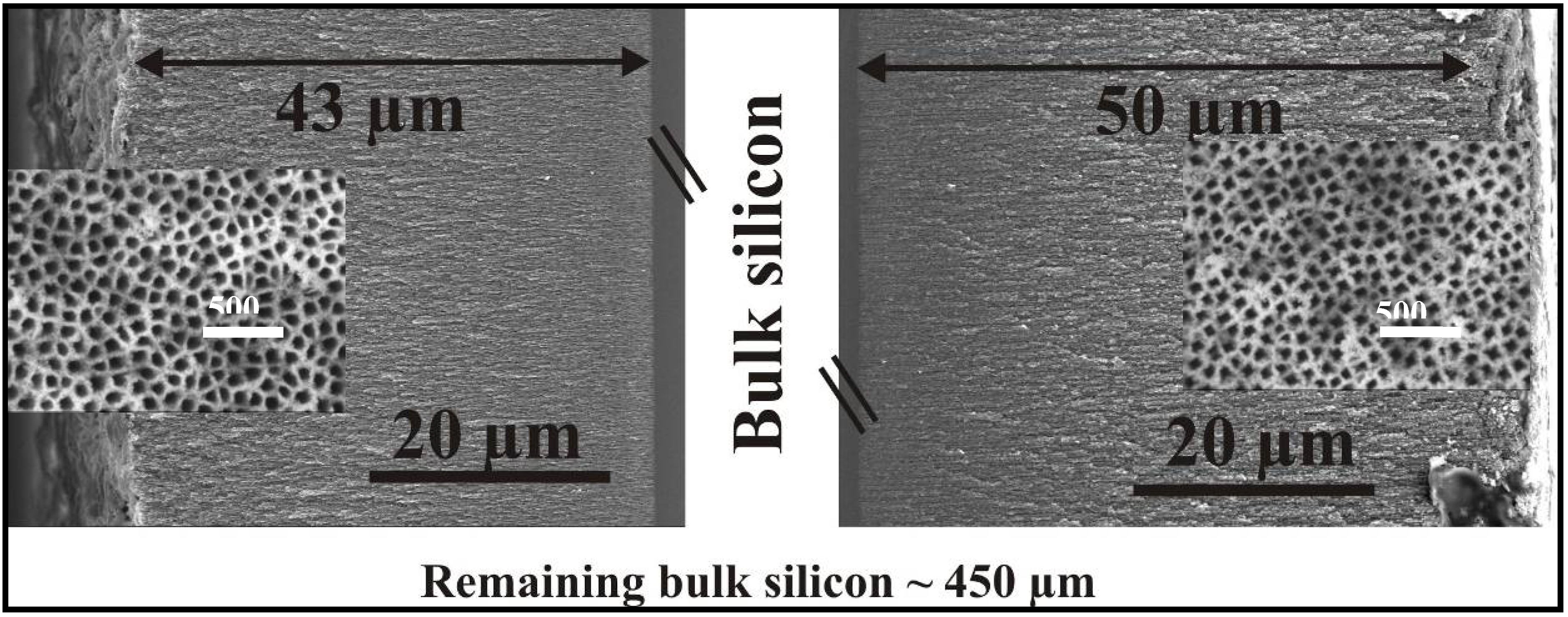
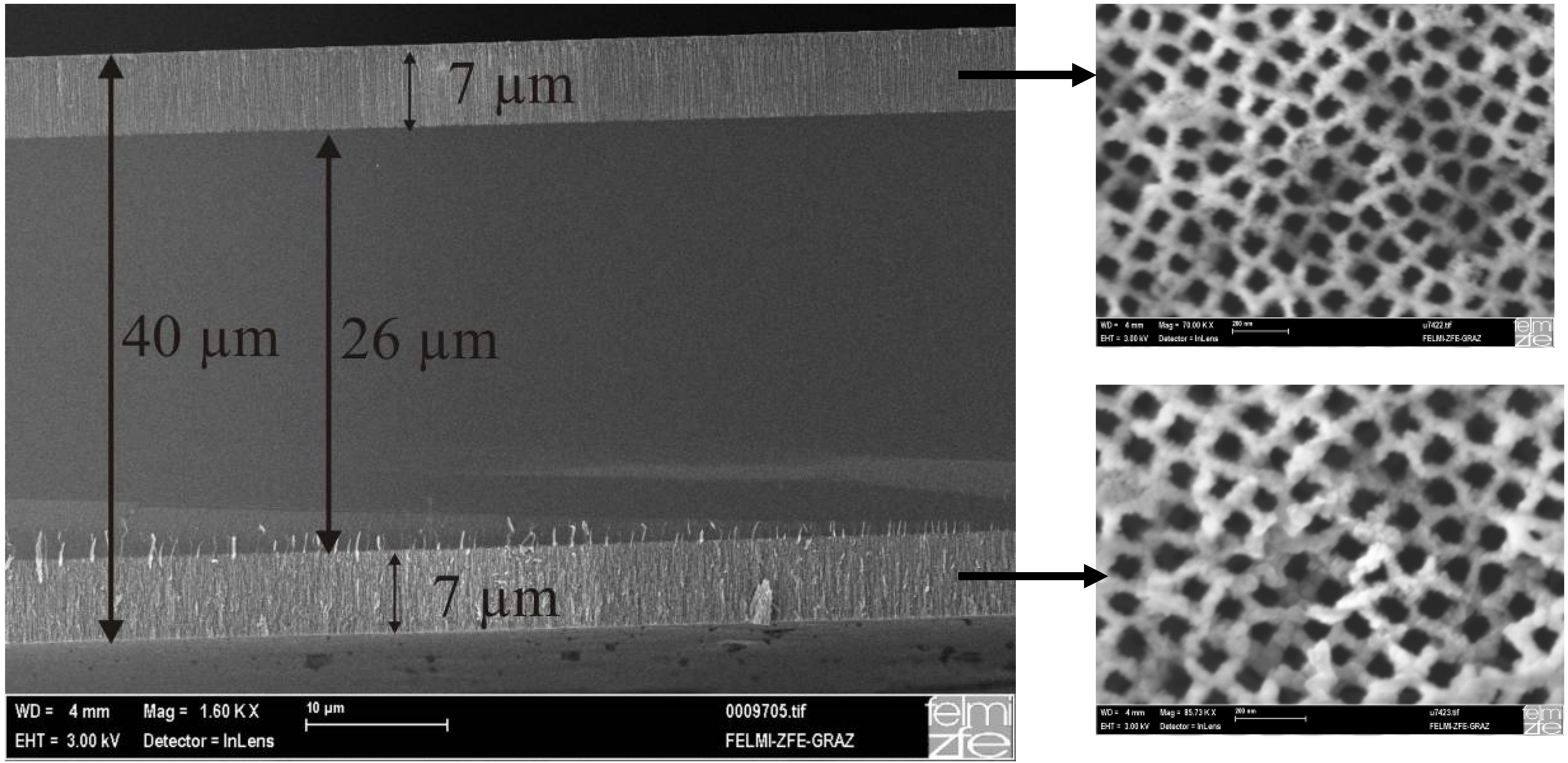
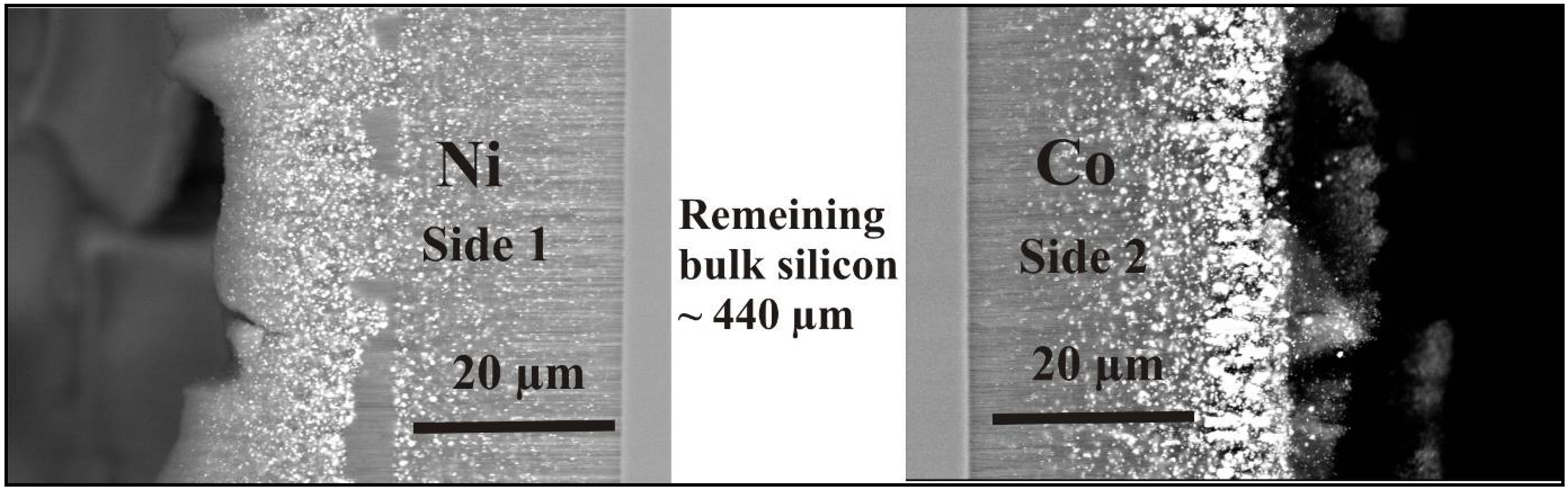
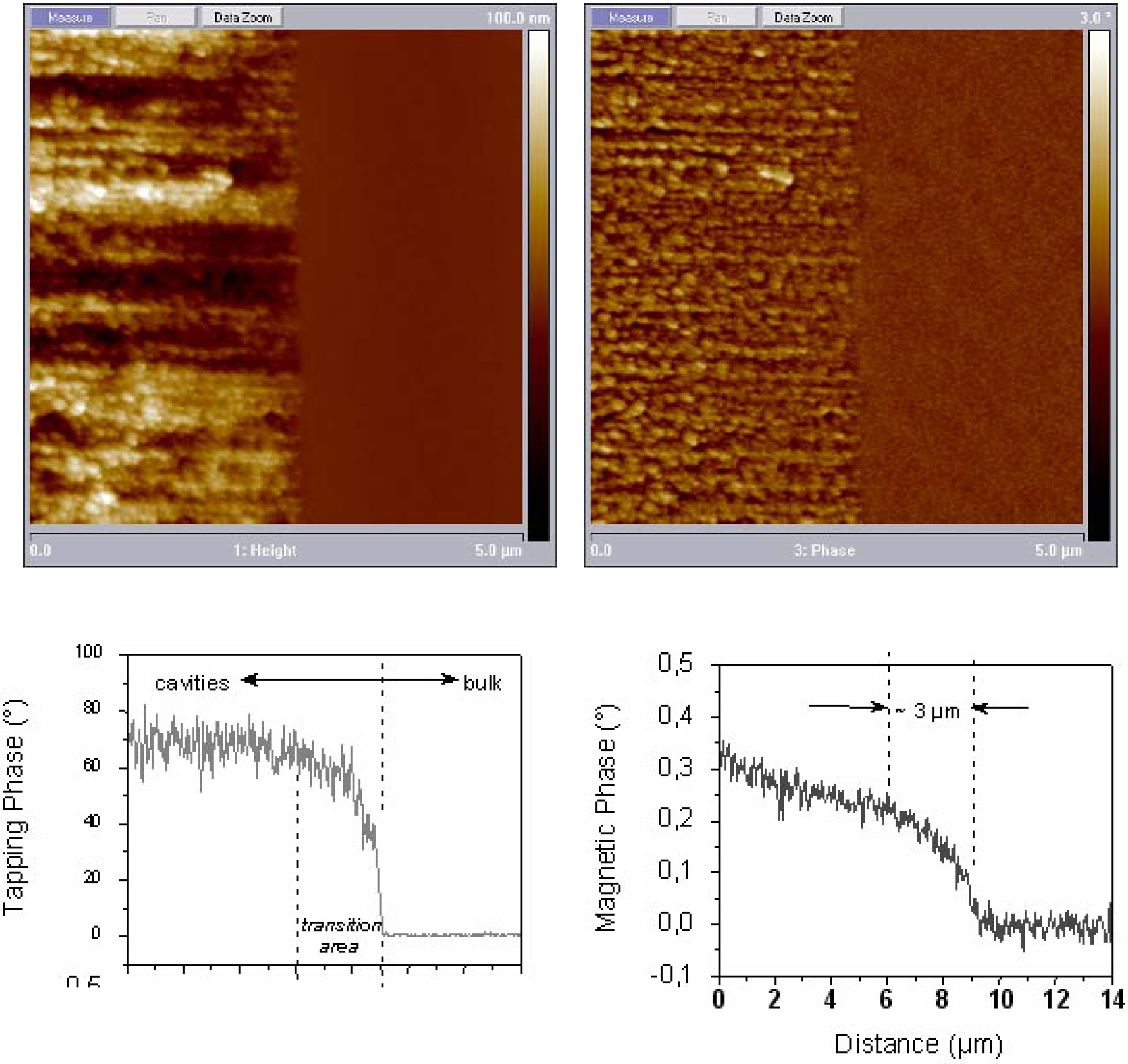
3. Double-Sided Porous Silicon Samples
Ultrathin wafers employed for double sided etching
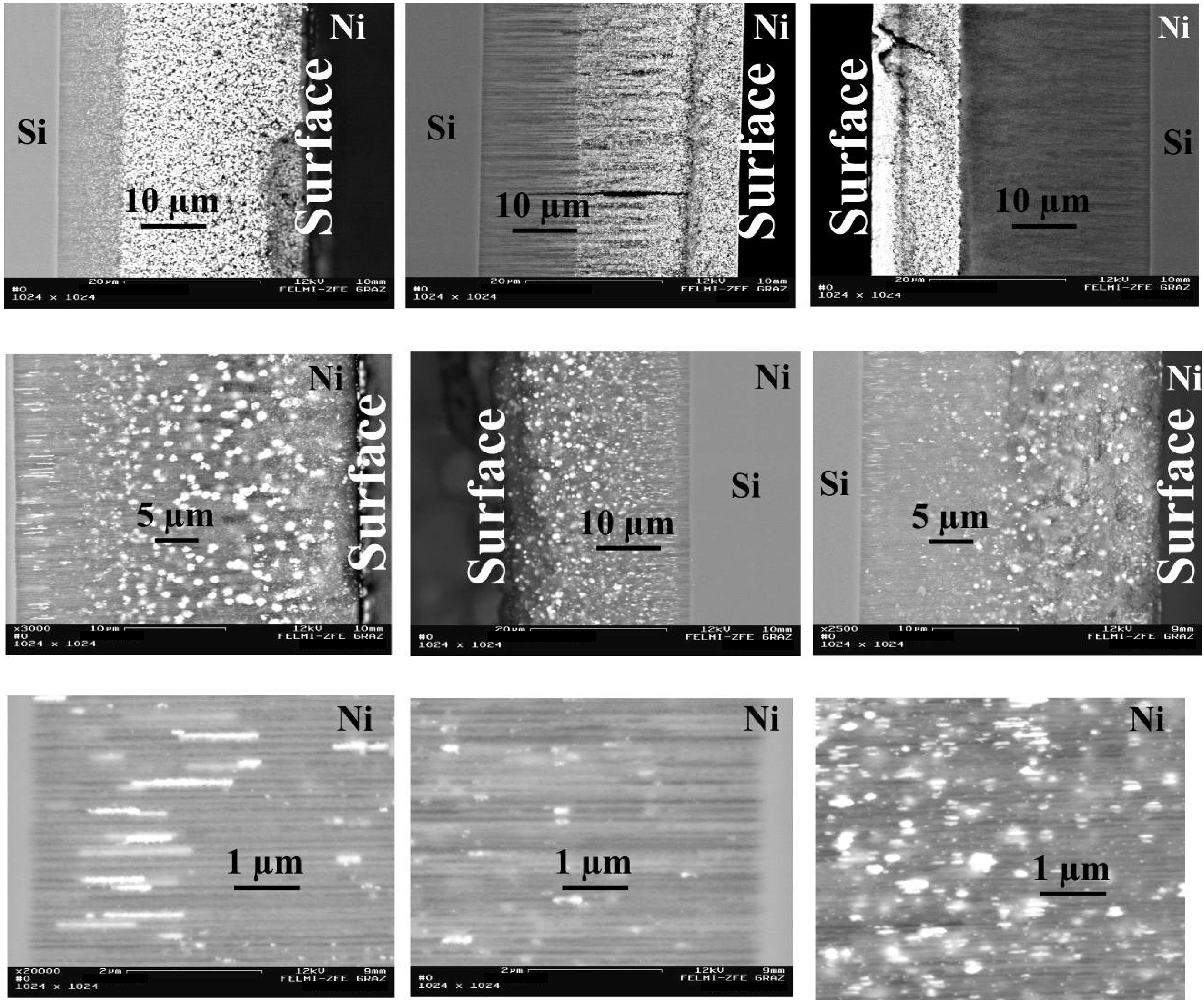
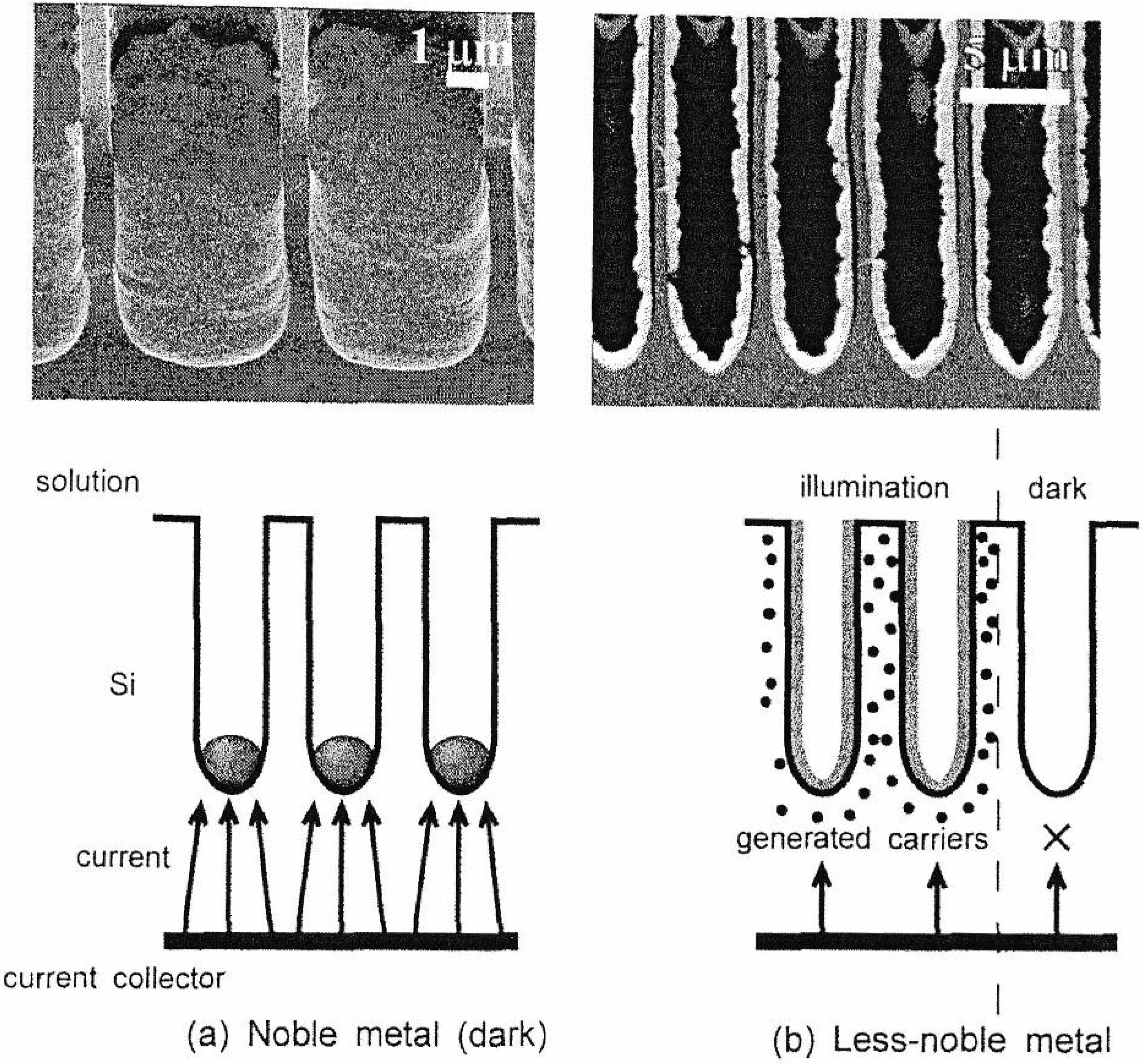
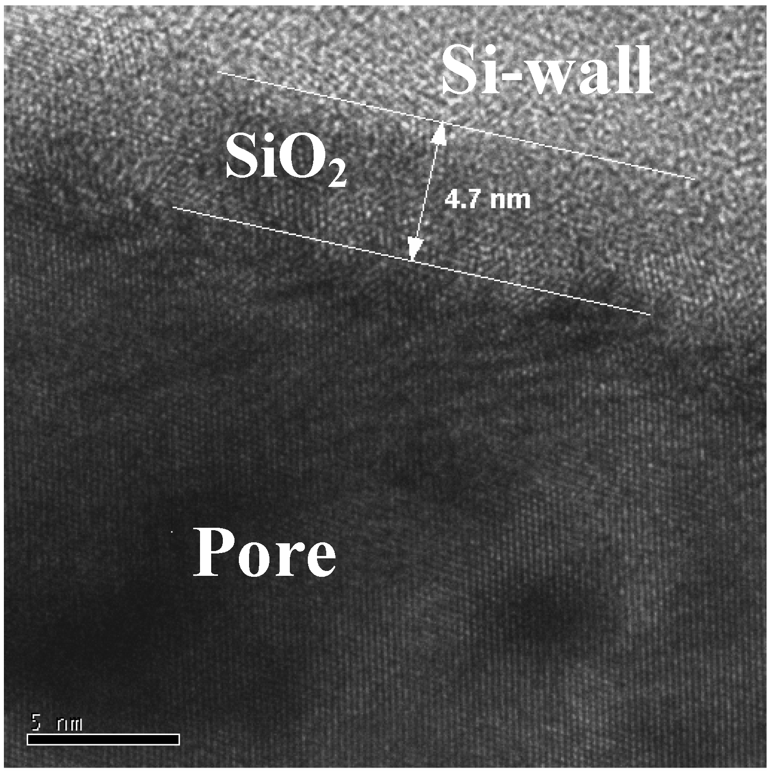
4. Filling of Porous Silicon
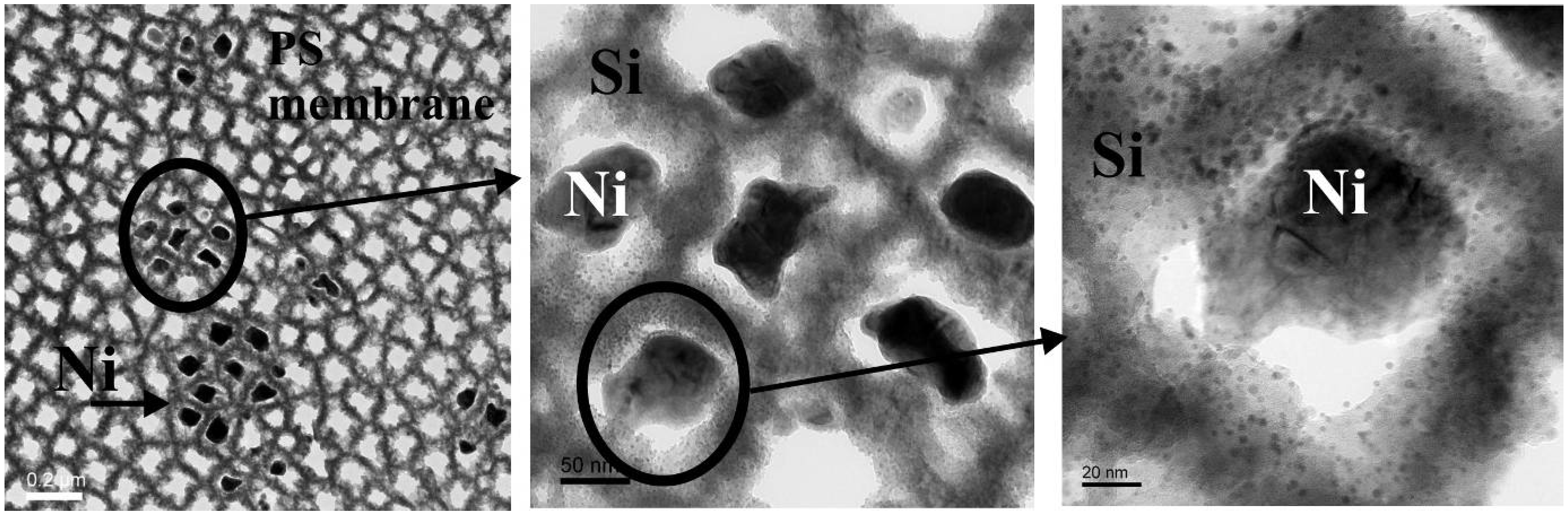
Metal deposition within porous silicon

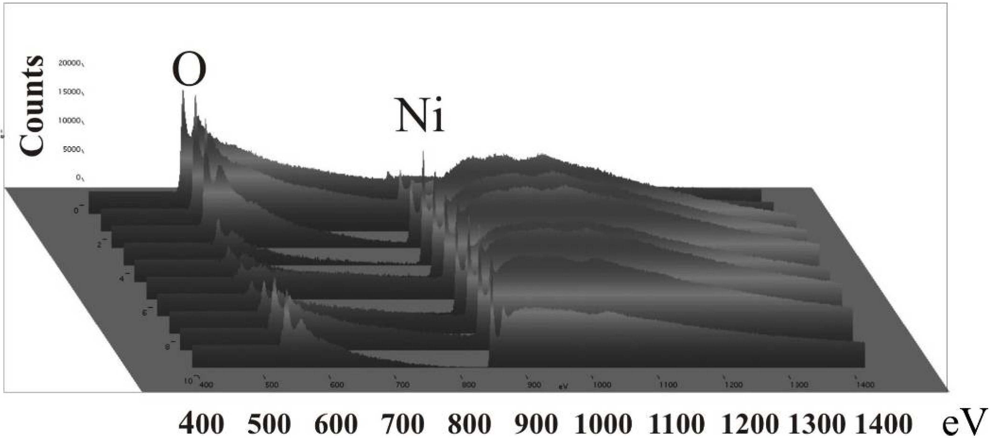
5. Deposition of Ferromagnetic Metals
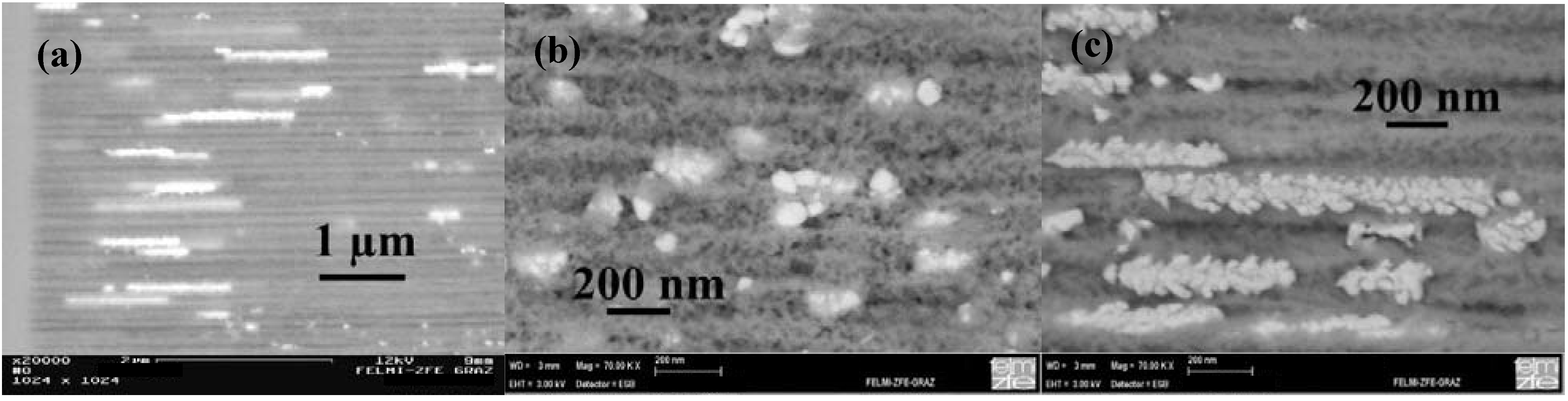
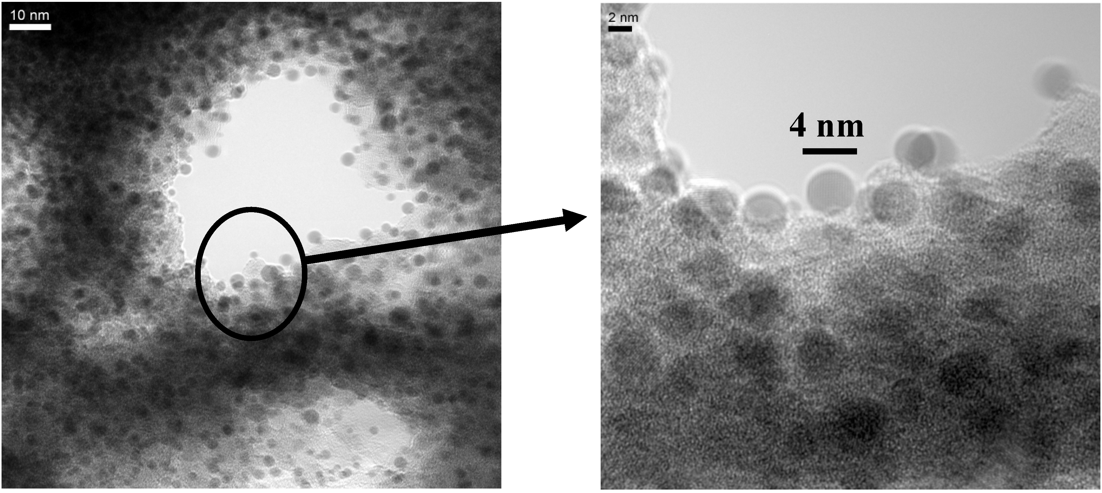
5.1. Pore filling
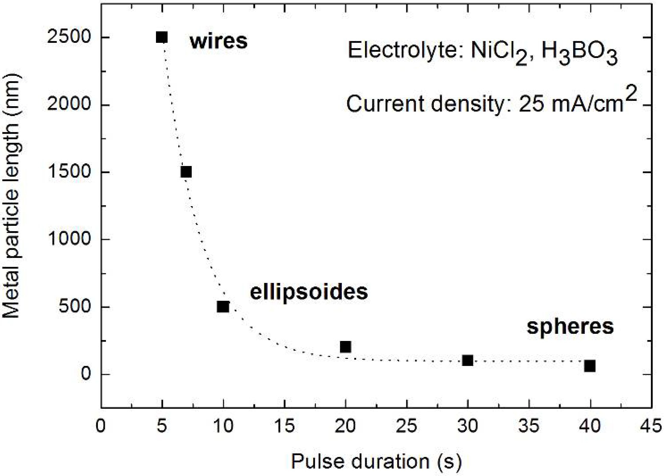
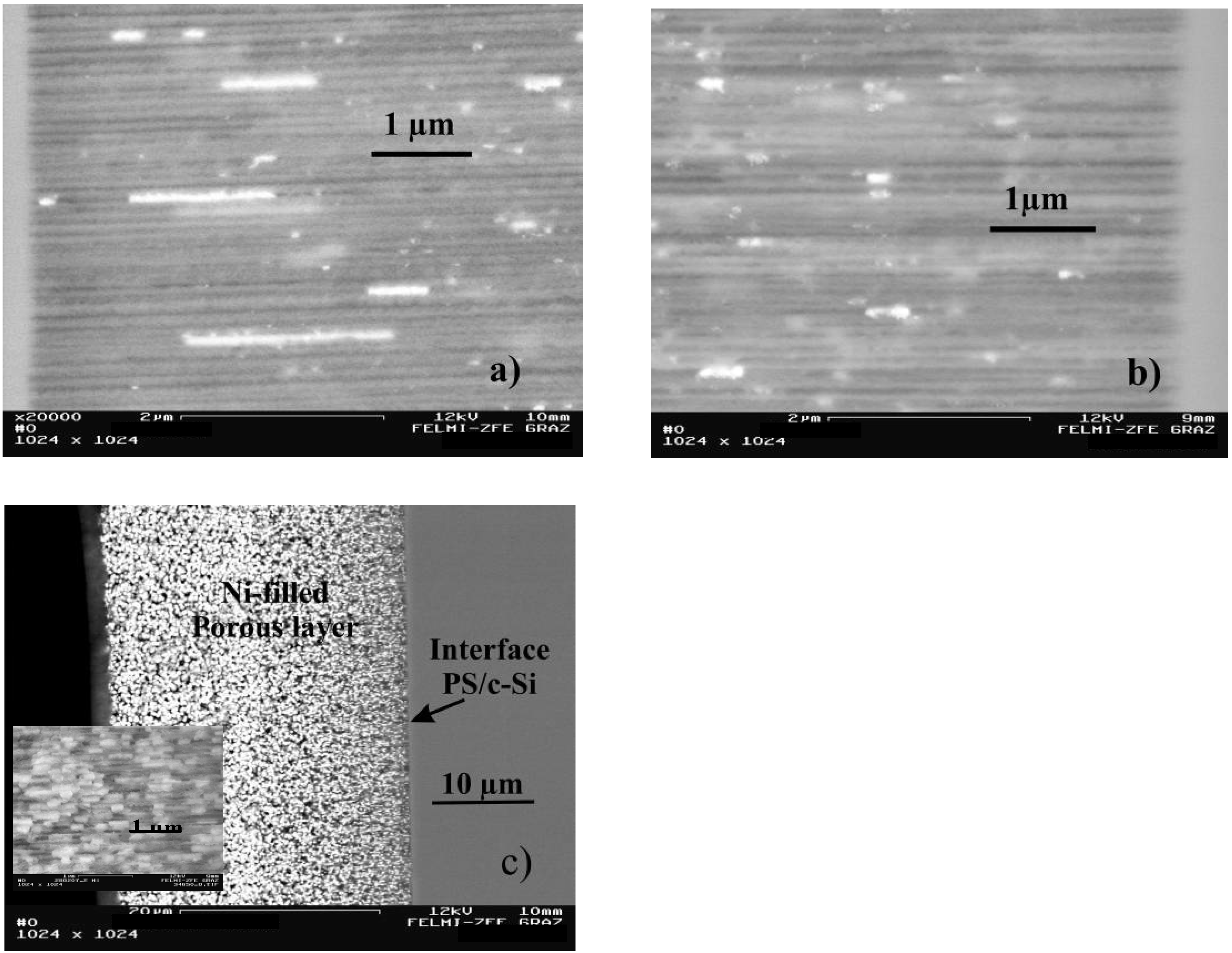
5.2. Nickel deposition within porous silicon
| Sample | Current density [mA/cm2] | Pulse duration [s] | Shape, elongation [nm] |
|---|---|---|---|
| 1 | 20 | 30 | Conglomerate |
| 2 | 40 | 20 | Particles, 200 |
| 3 | 40 | 5 | Wires , 2500 |


5.3. Cobalt deposition within porous silicon
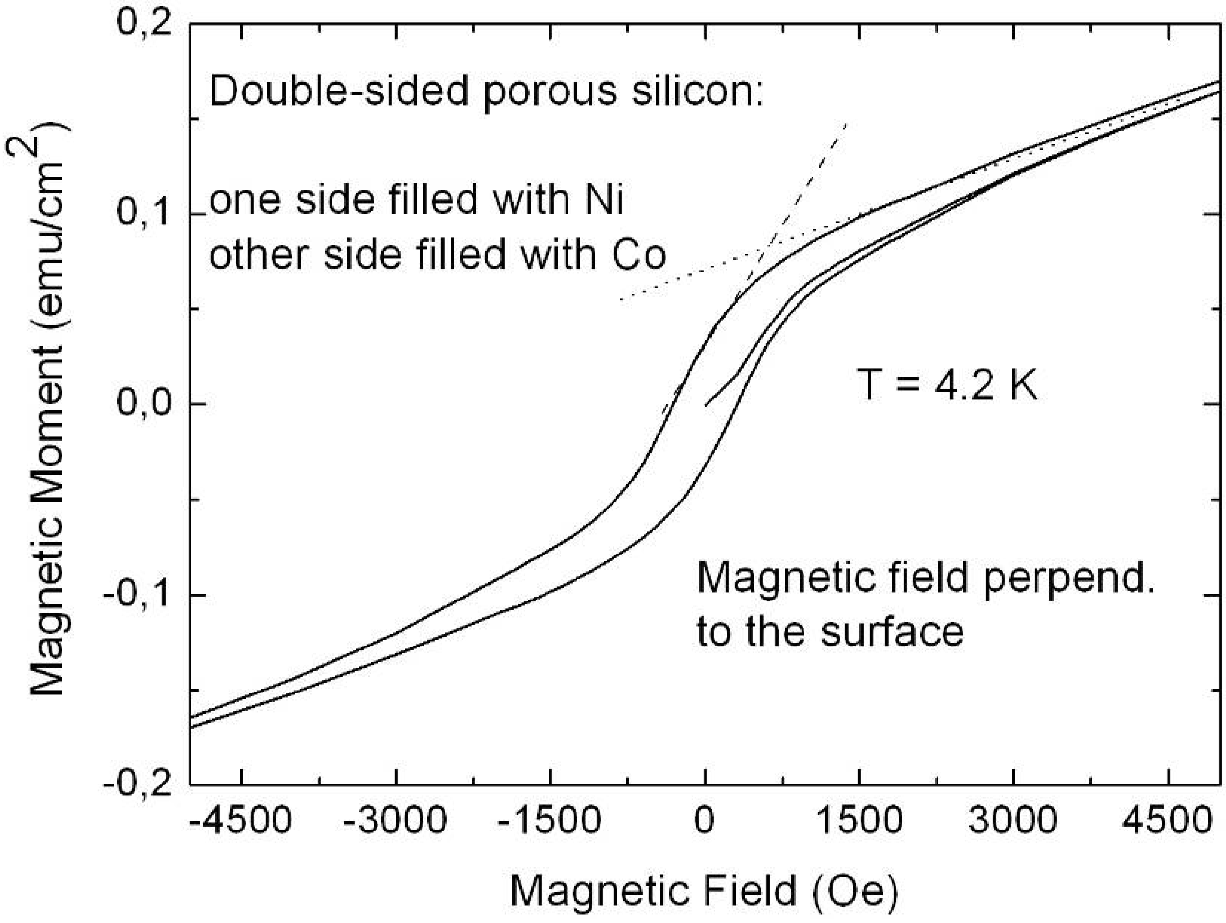
5.4. Metal-deposition within double-sided samples

6. Magnetic Characterization


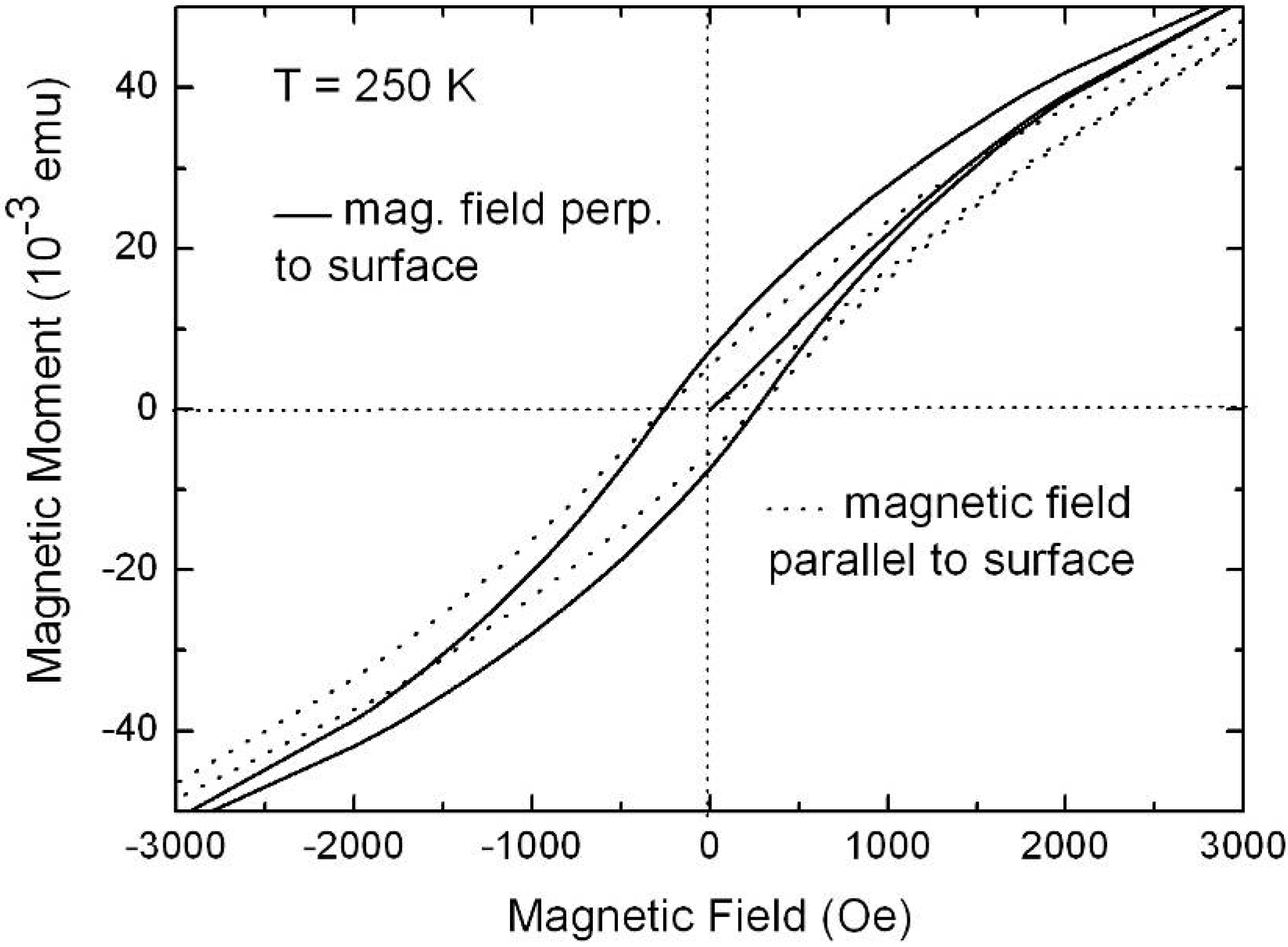
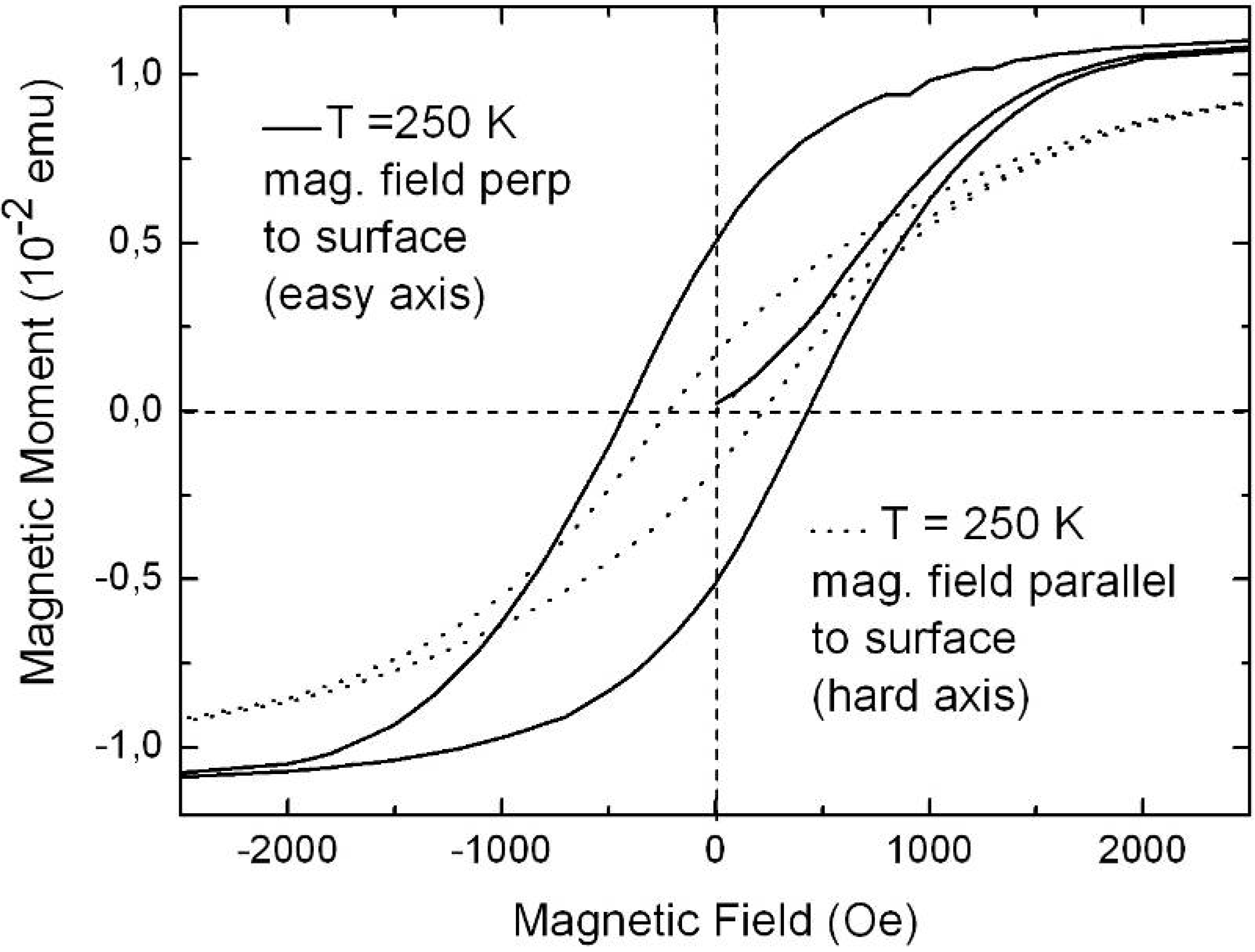
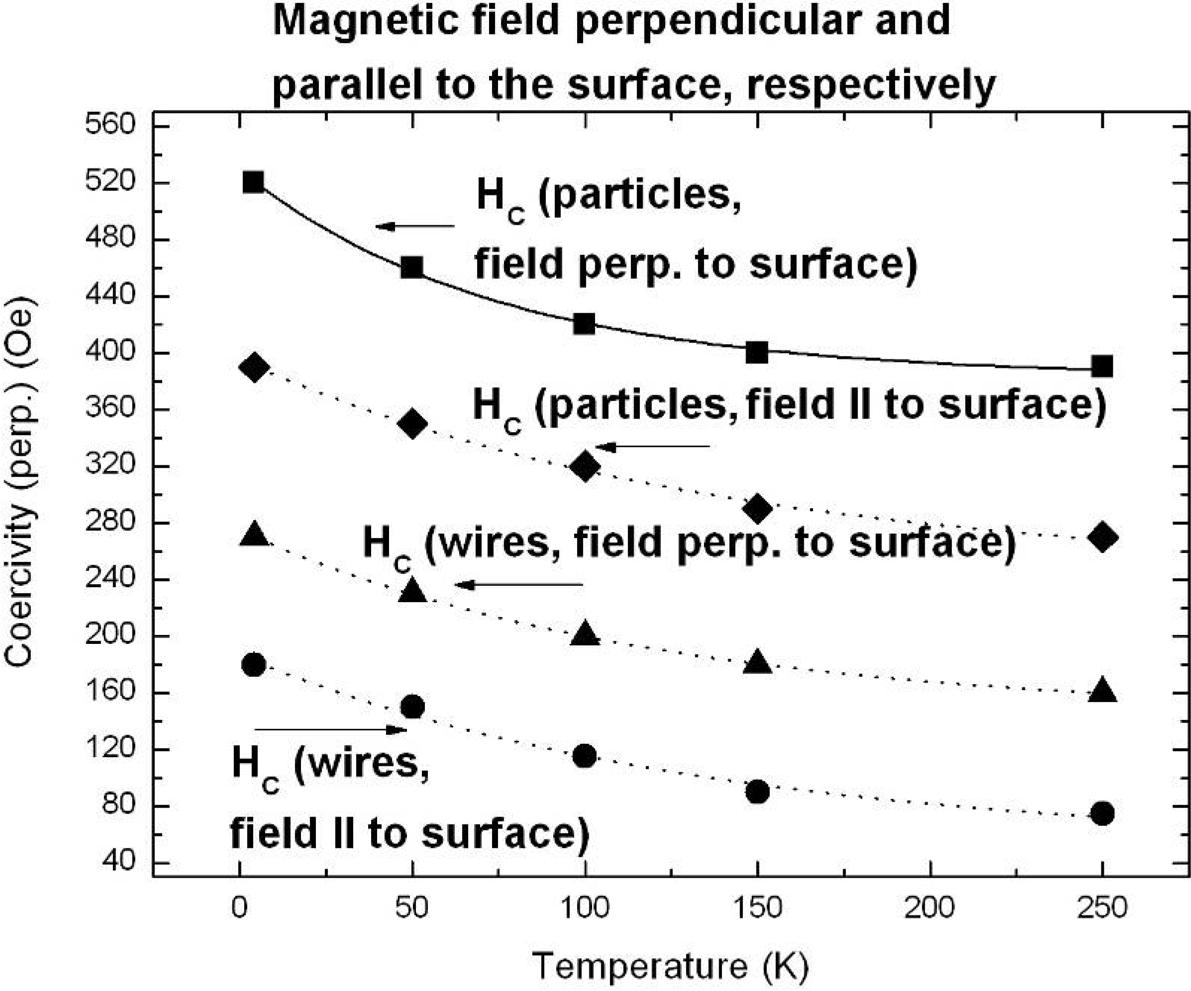
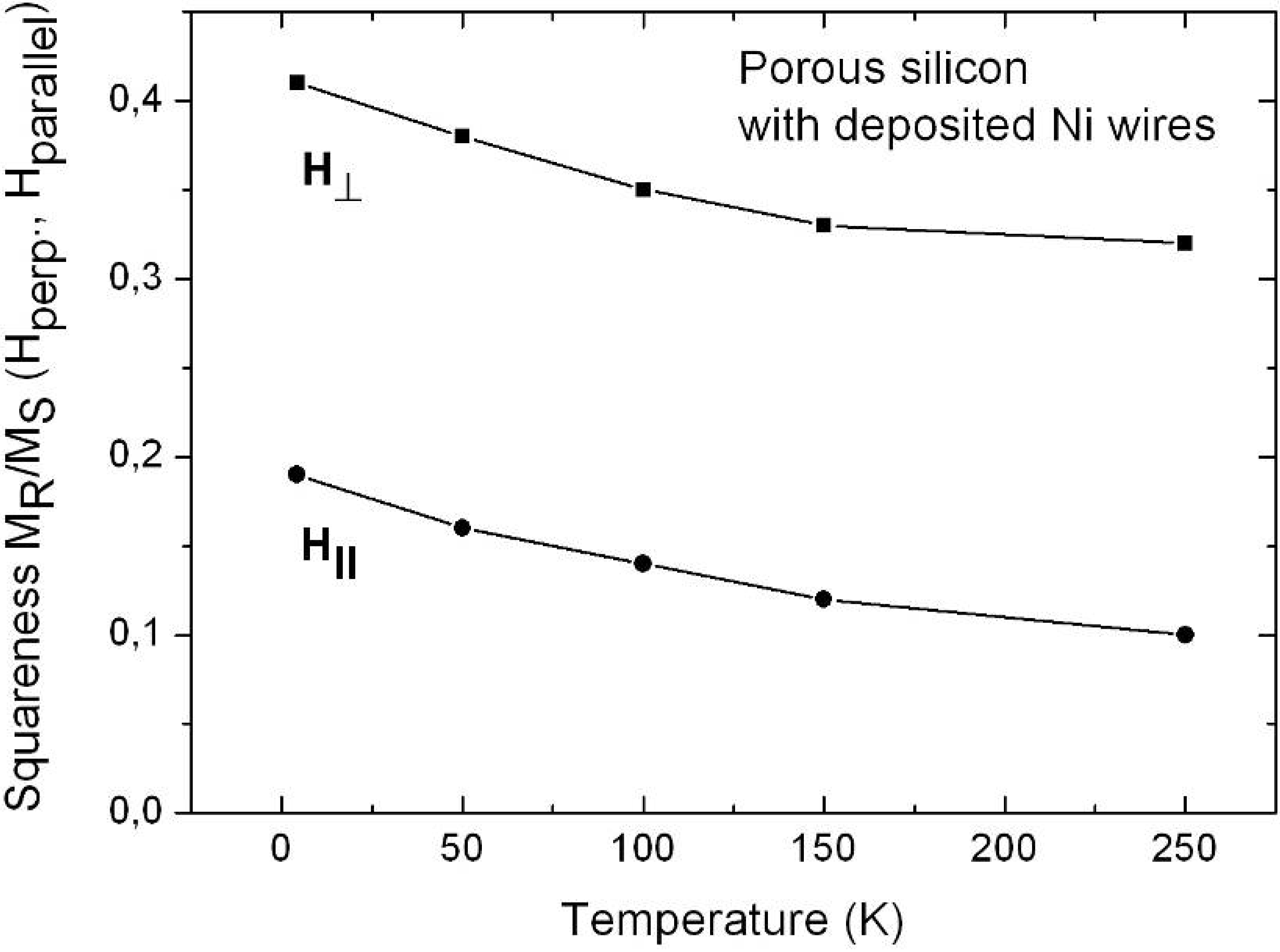
6.1. Correlation between morphology and magnetic properties
| MR/MS (4.2K, ‖) [%] | MR/MS (250K, ‖) [%] | MR/MS (4.2K,⊥) [%] | MR/MS (250K,⊥) [%] | |
|---|---|---|---|---|
| Ni-particles | 18 | 13 | 57 | 50 |
| Ni-wires | 19 | 10 | 41 | 32 |
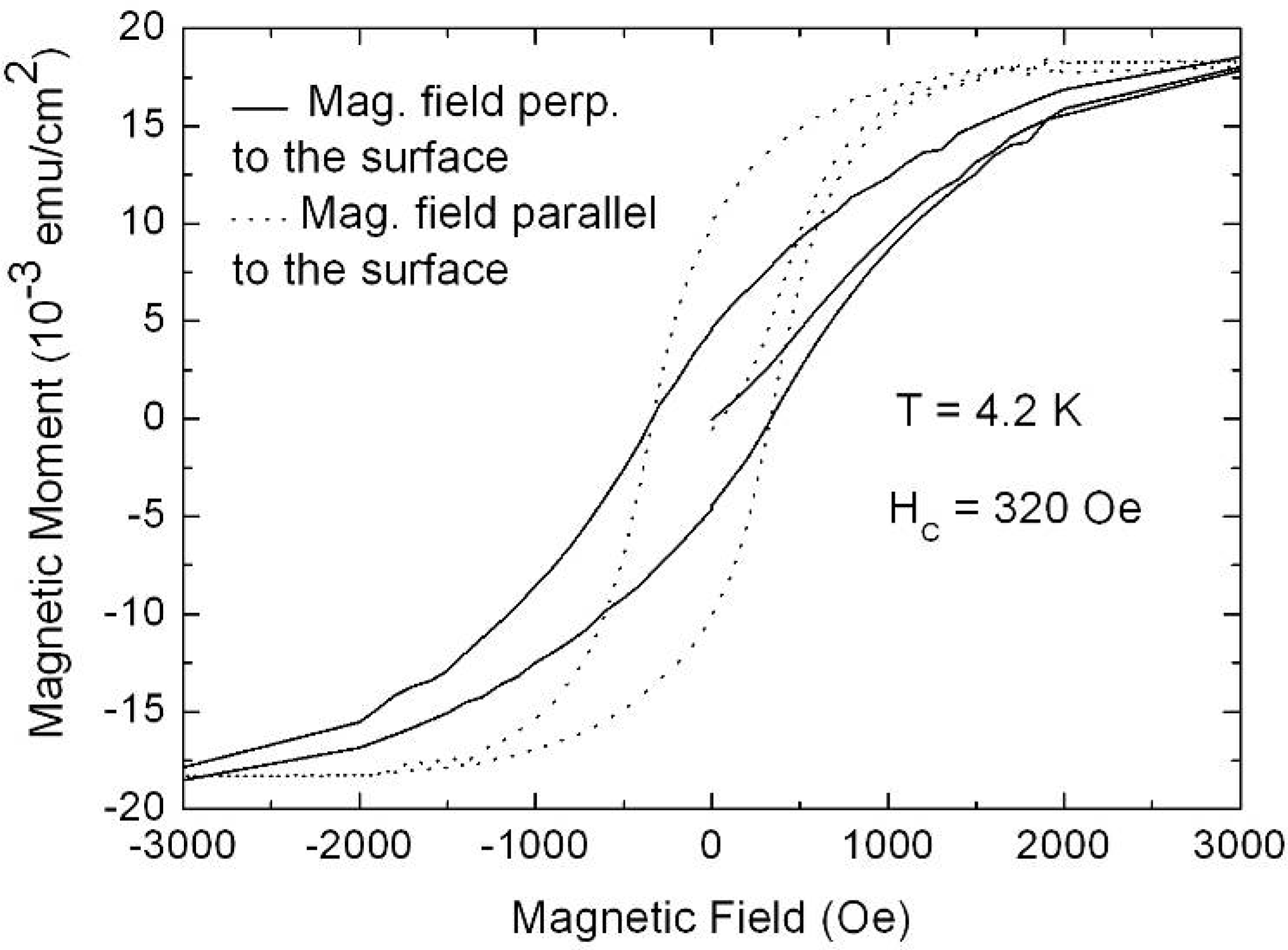
| T [K] | HC,⊥ [Oe] | HC,‖ [Oe] | MR,⊥ [emu] | (MR /MS)⊥ [%] | MR,‖ [emu] | (MR /MS)‖ [%] |
|---|---|---|---|---|---|---|
| 4.2 K | 500 | 480 | 0.01197 | 15 | 0.00985 | 12 |
| 100 K | 470 | 430 | 0.01161 | 16 | 0.0096 | 13 |
| 250 K | 260 | 250 | 0.00727 | 10 | 0.00536 | 7 |
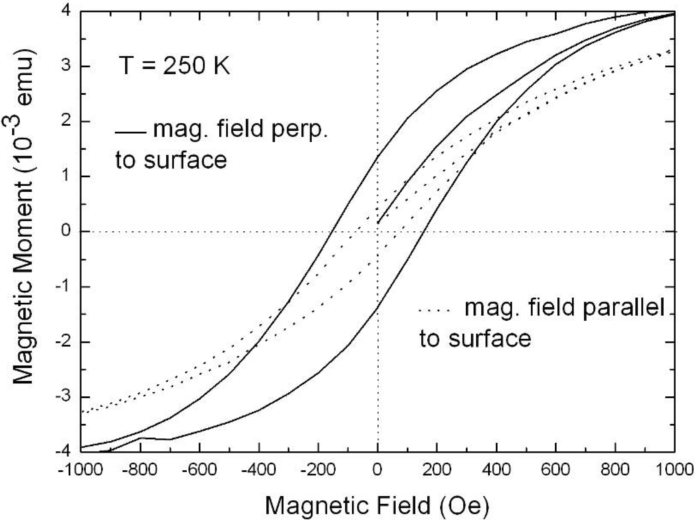
6.2. Temperature dependent magnetic behaviour

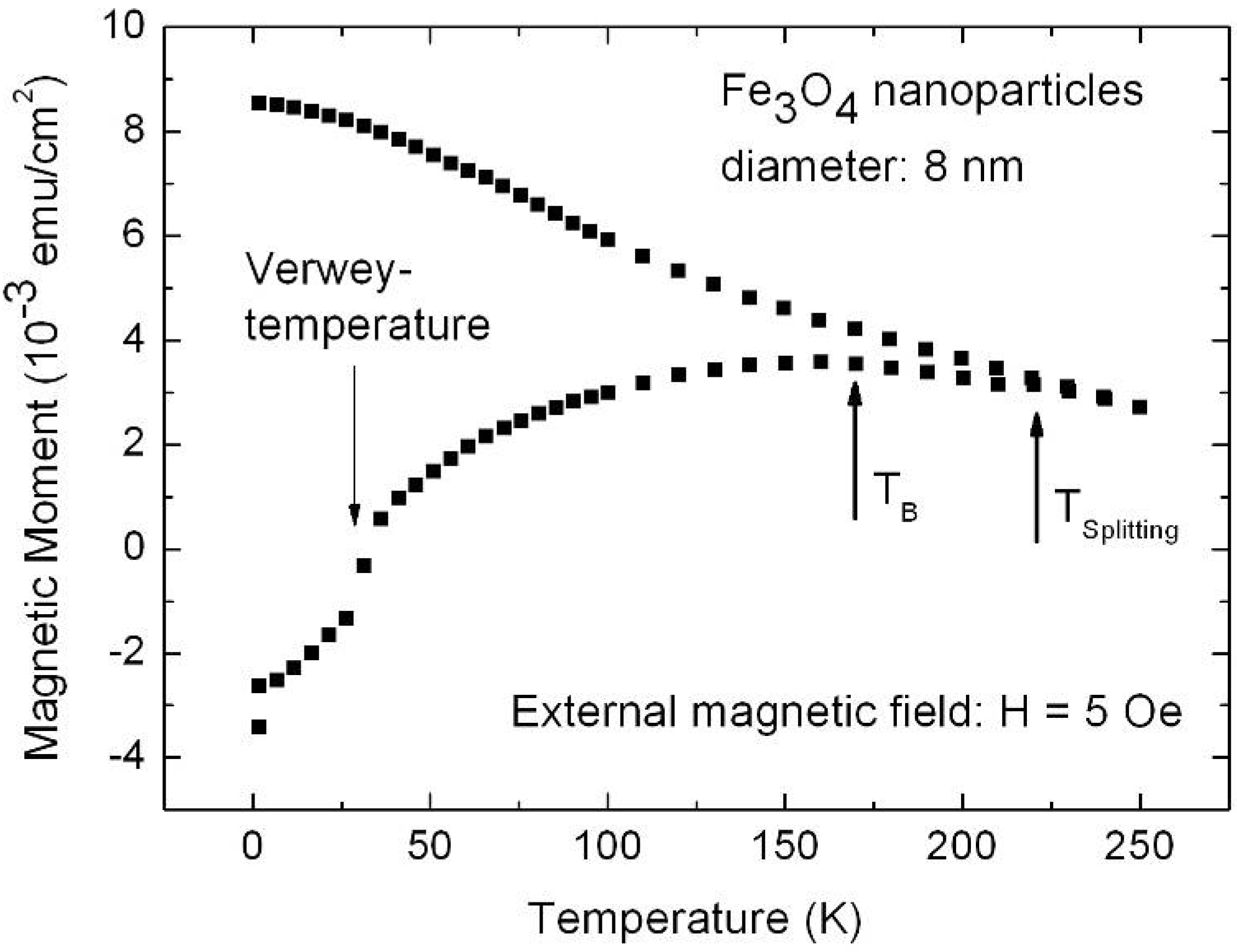
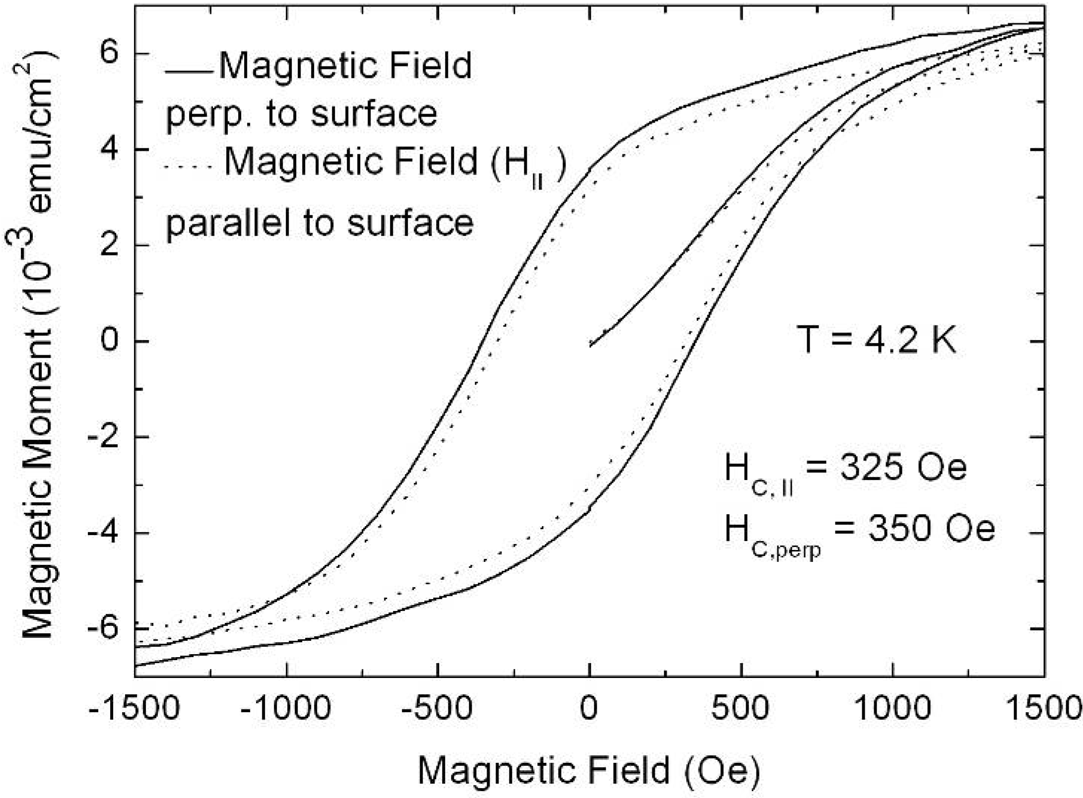
6.3. Microscopic investigations delivering further information about the magnetic behaviour

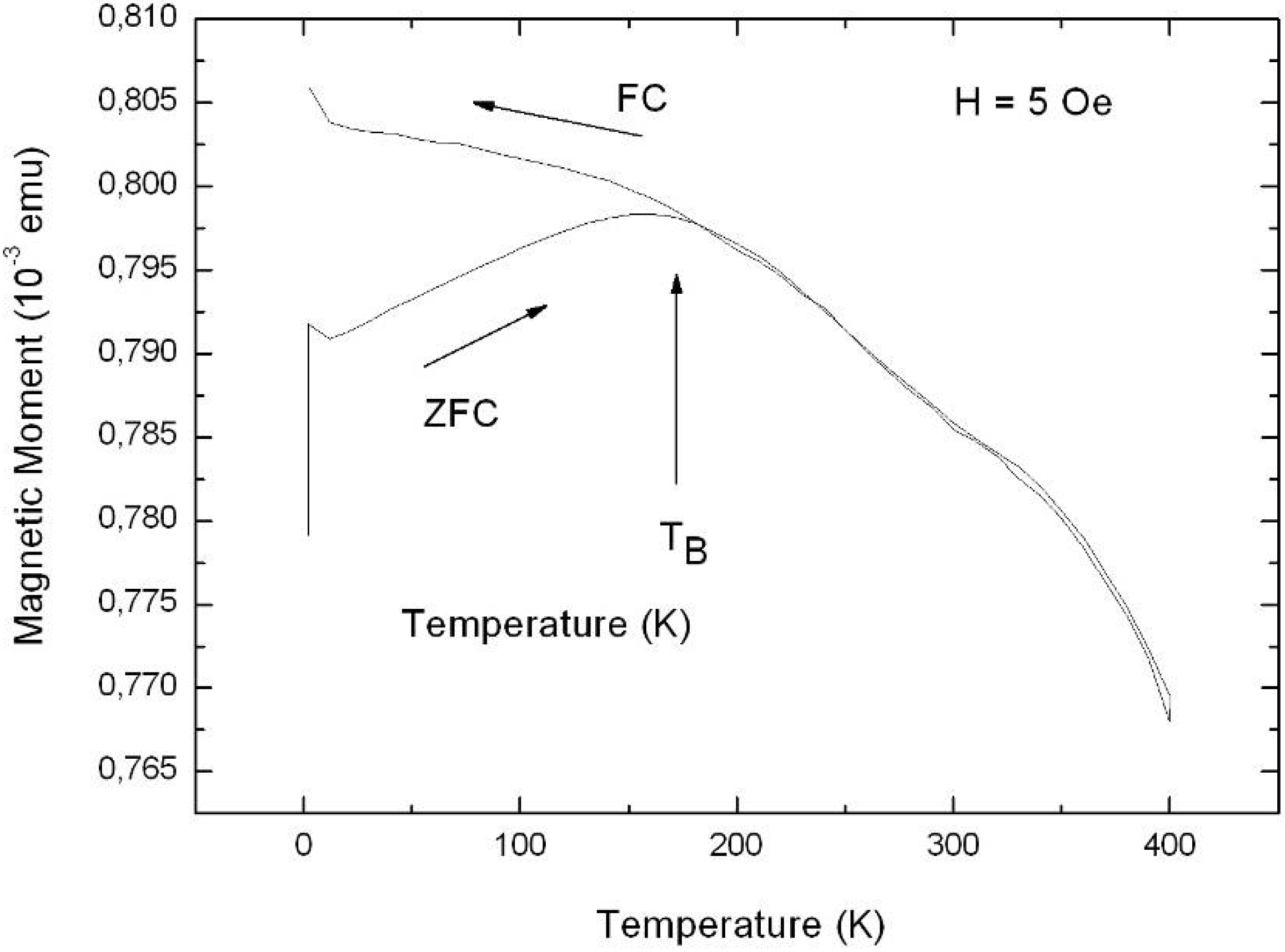
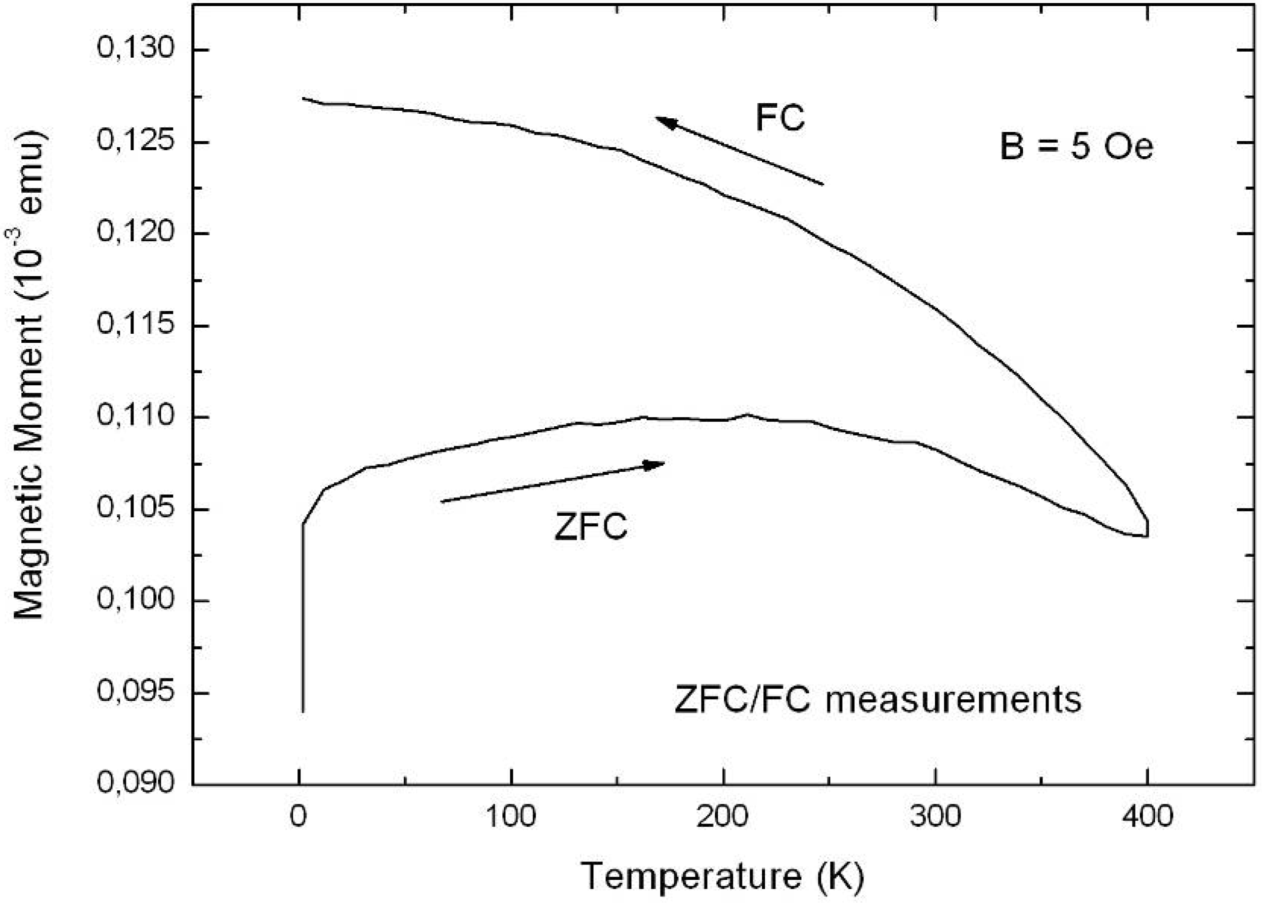
7. Porous Silicon/Fe3O4-Nanocomposite
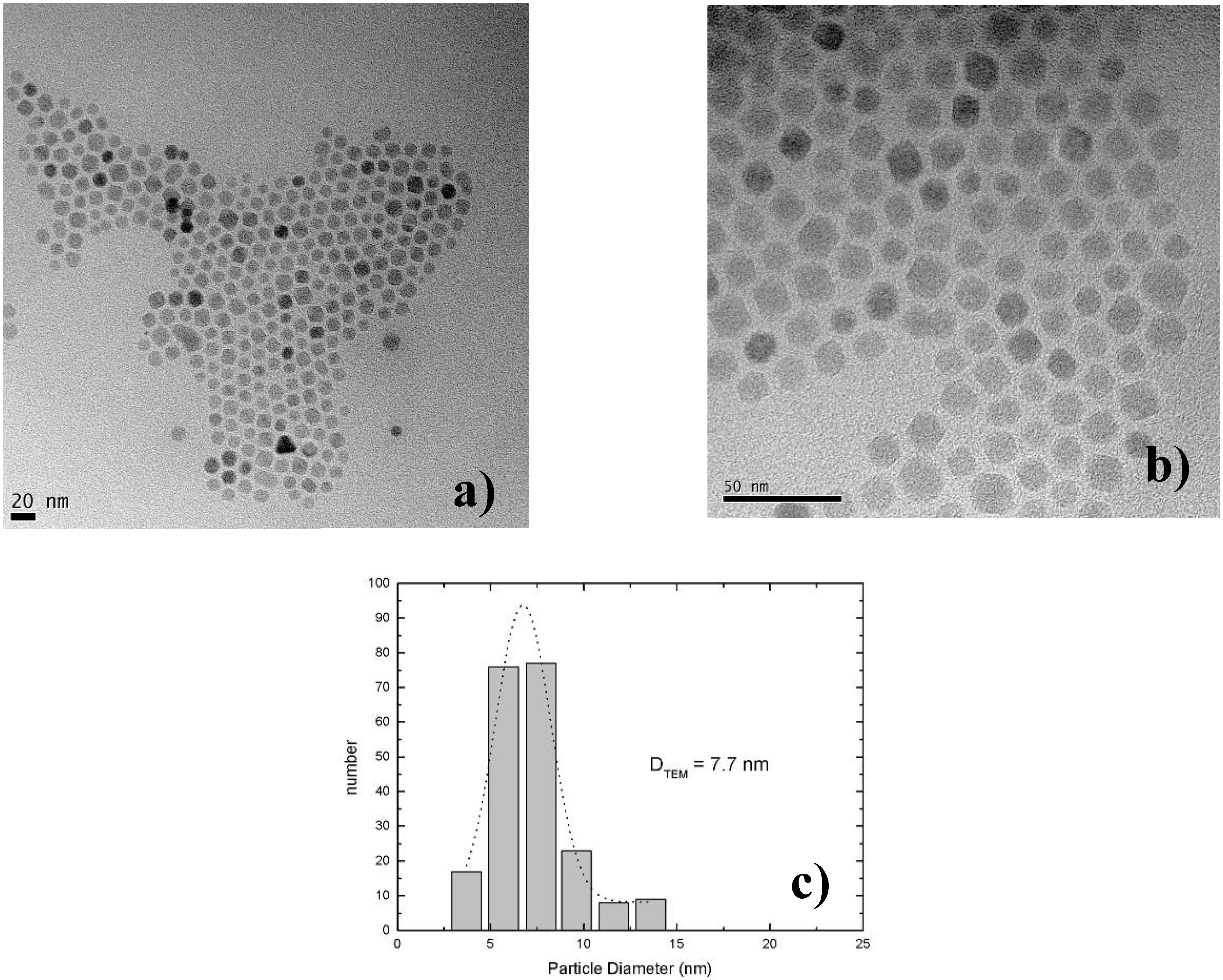
Influence of the porous silicon matrix
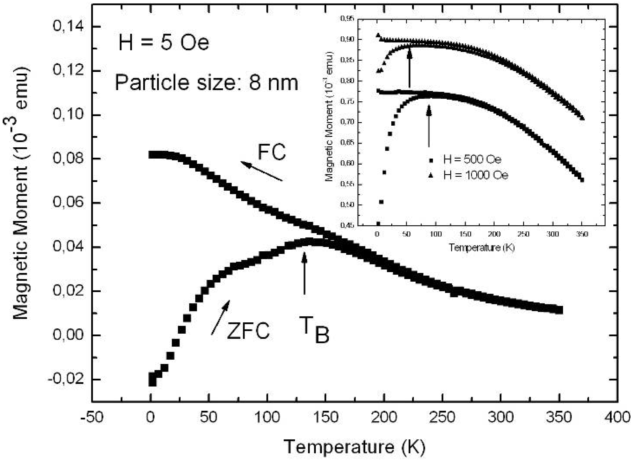
| H [Oe] | 5 | 500 | 1,000 |
| TB [K] | 135 | 75 | 55 |
- K … anisotropy constant
- V… volume of the particle
- MS … saturation magnetization
- HC … coercive field

8. Some Potential Uses of Porous Silicon
9. Conclusions
Acknowledgements
References and Notes
- Cowburn, R.P. Where have all the transistors gone? Science 2006, 311, 183–184. [Google Scholar] [CrossRef] [PubMed]
- Di Ventra, M.; Evoy, S.; Heflin, J.R., Jr. (Eds.) Introduction to Nanoscale Science and Technology; Nanostructure Science and Technology Series; Springer: New York, NY, USA, 2004.
- Allwood, D.A.; Xiong, G.; Cooke, M.D.; Cowburn, R.P. Magneto-optical Kerr effect analysis of magnetic nanostructures. J. Phys. D: Appl. Phys. 2003, 36, 2175–2182. [Google Scholar] [CrossRef]
- Han, G.C.; Zong, B.Y.; Wu, Y.H. Magnetic properties of magnetic nanowire arrays. IEEE Trans. Magn. 2002, 38, 2562–2564. [Google Scholar] [CrossRef]
- Ouyang, H.; Fauchet, Ph.M. Biosensing using porous silicon photonic bandgap structures. Proc. SPIE – Int. Soc. Opt. Eng. 2005, 6005, 6005081. [Google Scholar]
- Lundstrom, M. Applied Physics: Enhanced: Moore's Law Forever? Science 2003, 299, 210. [Google Scholar] [CrossRef] [PubMed]
- Yang, P. Nanotechnology: Wires on water. Nature 2003, 425, 243–243. [Google Scholar] [CrossRef] [PubMed]
- Shevchenko, E.V.; Talapin, D.V.; Kotov, N.A.; O'Brien, S.; Murray, C.B. Structural diversity in binary nanoparticle superlattices. Nature 2006, 439, 55–59. [Google Scholar] [CrossRef] [PubMed]
- Masuda, H.; Yotsuya, M.; Ishida, M. Spatially selective metal deposition into a hole-array structure of anodic alumina using a microelectrode. Jpn. J. Appl. Phys. 1998, 37, L1090–L1092. [Google Scholar] [CrossRef]
- Grom, G.F.; Lockwood, D.J.; McCaffrey, J.P.; Labbe, H.J.; Fauchet, P.M.; White, B., Jr.; Dinier, J.; Kovalev, D.; Koch, F.; Tsybeskov, L. Ordering and self-organization in nanocrystalline silicon. Nature 2000, 407, 358–361. [Google Scholar] [CrossRef] [PubMed]
- Hierold, Ch. Carbon Nanotubes Devices, Properties, Modelling, Integration and Application; Wiley-VCH: Weinheim, Germany, 2008; Volume 8, Advanced Micro- and Nanosystems. [Google Scholar]
- Song, Y.Y.; Lynch, R.; Kim, D.; Roy, P.; Schmuki, P. TiO2 nanotubes: Efficient suppression of top etching during anodic growth. Electrochem. Solid-State Lett. 2009, 12, C17–C20. [Google Scholar] [CrossRef]
- Pastor, E.; Matveeva, E.; Parkhutik, V.; Curiel-Esparza, J.; Millan, M.C. Influence of porous silicon oxidation on its behaviour in simulated body fluid. Phys. Status Solidi C 2007, 4, 2136–2140. [Google Scholar] [CrossRef]
- Canham, L.T. Porous silicon as a therapeutic biomaterial. In IEEE Conference on Microtechnologies in Medicine and Biology, Lyon, France, 12–14 October 2000.
- Chazalviel, J.-N.; Ozanam, F.; Gabouze, N.; Fellah, S.; Wehrspohn, R.B. Quantitative analysis of the morphology of macropores on low-doped p-Si. J. Electrochem. Soc. 2002, 149, C511–C520. [Google Scholar] [CrossRef]
- Uhlir, A., Jr. Electrolytic shaping of Germanium and Silicon. Bell System Tech. J. 1956, 35, 333–347. [Google Scholar] [CrossRef]
- Turner, R. Electropolishing silicon in hydrofluoric acid solution. J. Electochem. Soc. 1958, 105, 402–408. [Google Scholar] [CrossRef]
- Canham, L.T. Silicon quantum wire array fabrication by electrochemical and chemical dissolution of wafers. Appl. Phys. Lett. 1990, 57, 1046–1048. [Google Scholar] [CrossRef]
- Lehmann, V.; Jobst, B.; Muschik, Th.; Kux, A.; Petrova-Koch, V. Correlation between optical properties and crystallite size in porous silicon. Japn. J. Appl. Phys. 1993, 32, 2095–2099. [Google Scholar] [CrossRef]
- Harvey, J.F.; Shen, H.; Lux, R.A.; Dutta, M.; Pamulapati, J.; Tsu, R. Raman and optical characterization of porous silicon. Mat. Res. Soc. Symp. Proc. 1992, 256, 175. [Google Scholar] [CrossRef]
- Ito, T.; Ohta, T.; Hiraki, A. Light emission from microcrystalline Si confined in SiO2 matrix through partial oxidation of anodized porous silicon. Japn. J. Appl. Phys. 1992, 31, L1–L3. [Google Scholar] [CrossRef]
- Hou, X.Y.; Shi, G.; Wang, W.; Zhang, F.L.; Hao, P.H. Blue light emission from porous silicon. Mat. Res. Soc. Symp. 1993, 283, 89–93. [Google Scholar] [CrossRef]
- Koch, F.; Petrova-Koch, V. The Surface State Mechanism for Light Emission from Porous Silicon. In Porous Silicon; Feng, Z.C., Tsu, R., Eds.; World Scientific: Singapore, 1994. [Google Scholar]
- Jiang, D.T.; Coulthard, I.; Sham, T.K.; Lorimer, J.W.; Frigo, S.P.; Feng, X.H.; Rosenberg, R.A. Observations on the surface and bulk luminescence of porous silicon. J. Appl. Phys. 1993, 74, 6335–6340. [Google Scholar] [CrossRef]
- Tamura, H.; Rückschloss, M.; Wirschem, Th.; Veprek, S. Origin of the green/blue luminescence from nanocrystalline silicon. Appl. Phys. Lett. 1994, 65, 1537. [Google Scholar] [CrossRef]
- Lehmann, V. Electrochemistry of Silicon, Instrumentation, Science, Materials and Applications; Wiley-VCH: Weinheim, Germany, 2002. [Google Scholar]
- Föll, H.; Christophersen, M.; Carstensen, J.; Hasse, G. Formation and application of porous silicon. Mater. Sci. Eng. 2002, R39, 93–141. [Google Scholar] [CrossRef]
- Chazalviel, J.-N. The silicon/electrolyte interface. In Porous Silicon Science and Technology; Winter School Les Houches 8–12 February, Les Editions de Physique; Vial, J.-C., Derrien, J., Eds.; Springer: New York, NY, USA, 1995. [Google Scholar]
- Halimaoui, A. Porous Silicon: material processing, properties and applications. In Porous Silicon: Material Processing, Properties and Applications; Winter School Les Houches 8–12 February, Les Editions de Physique; Vial, J.-C., Derrien, J., Eds.; Springer: New York, NY, USA, 1995. [Google Scholar]
- Gösele, U.; Lehmann, V. Porous Silicon Quantum Sponge Structures: Formation Mechanism, Preparation Methods and some Properties. In Porous Silicon; Feng, Z.C., Tsu, R., Eds.; World Scientific: Singapore, 1994. [Google Scholar]
- Lehmann, V.; Rönnebeck, S. The physics of macropore formation in low doped p-type silicon. J. Electrochem. Soc. 1999, 146, 2968–2975. [Google Scholar] [CrossRef]
- Lehmann, V.; Grüning, U. The limits of macropore array fabrication. Thin Solid Films 1997, 297, 13–17. [Google Scholar] [CrossRef]
- Lehmann, V. The physics of macropore formation in low doped n-type silicon. J. Electrochem. Soc. 1993, 140, 2836–2843. [Google Scholar] [CrossRef]
- Lehmann, V.; Föll, H. Formation mechanism and properties of electrochemically etched trenches in n-type silicon. J. Electrochem. Soc. 1990, 137, 653–659. [Google Scholar] [CrossRef]
- Ouyang, H.; Christophersen, M.; Fauchet, Ph.M. Enhanced control of porous silicon morphology from macropore to mesopore formation. Phys. Status Solidi A 2005, 202, 1396–1401. [Google Scholar] [CrossRef]
- Parkhutik, V. Porous silicon – mechanisms of growth and applications. Solid State Electron. 1999, 43, 1121–1141. [Google Scholar] [CrossRef]
- Lauerhaas, J.M.; Sailor, M.J. Chemical modification of the photoluminescence quenching of porous silicon. Science 1993, 261, 1567–1568. [Google Scholar] [CrossRef] [PubMed]
- Anglin, E.J.; Cheng, L.; Freeman, W.R.; Sailor, M.J. Porous silicon in drug delivery devices and materials. Adv. Drug Deliv. Rev. 2008, 60, 1266–1277. [Google Scholar] [CrossRef] [PubMed]
- Canham, L.T.; Stewart, M.P.; Buriak, J.M.; Reeves, C.L.; Anderson, M.; Squire, E.K.; Allock, P.; Snow, P.A. Derivatized porous silicon mirrors: Implantable optical components with slow resorbability. Phys. Status Solidi A Appl. Res. 2000, 182, 521–525. [Google Scholar] [CrossRef]
- Canham, L.T. Nanoscale semiconducting silicon as a nutritional food additive. Nanotechnology 2007, 18, 1–6. [Google Scholar] [CrossRef]
- Lee, X.; Coffer, J.; Chen, Y.; Pinizotto, R.F.; Newey, J.; Canham, L.T. Transition metal complex doped hydroxyapatite layers on porous silicon. J. Am. Chem. Soc. 1999, 120, 11706–11709. [Google Scholar]
- Herino, R. Impregnation of porous silicon. In Properties of Porous Silicon; Canham, L., Ed.; INSPEC: London, UK, 1997. [Google Scholar]
- Huang, Y.M. Photoluminescence of copper-doped porous silicon. Appl. Phys. Lett. 1996, 69, 2855–2857. [Google Scholar] [CrossRef]
- Zacharatos, F.; Nassiopoulou, A.G. Copper-filled macroporous Si and cavity underneath for microchannel heat sink technology. Phys. Status Solidi A Appl. Res. 2008, 205, 2513–2517. [Google Scholar] [CrossRef]
- Granitzer, P.; Rumpf, K.; Pölt, P.; Simic, S.; Krenn, H. Three-dimensional quasi-regular arrays of Ni nanostructures grown within the pores of a porous silicon layer - magnetic characteristics. Phys. Status Solidi C 2008, 5, 3580–3583. [Google Scholar] [CrossRef]
- Lehmann, V.; Hönlein, W.; Reisinger, H.; Spitzer, A.; Wendt, H.; Willer, J. A novel capacitor technology based on porous silicon. Thin Solid Films 1996, 276, 138–142. [Google Scholar] [CrossRef]
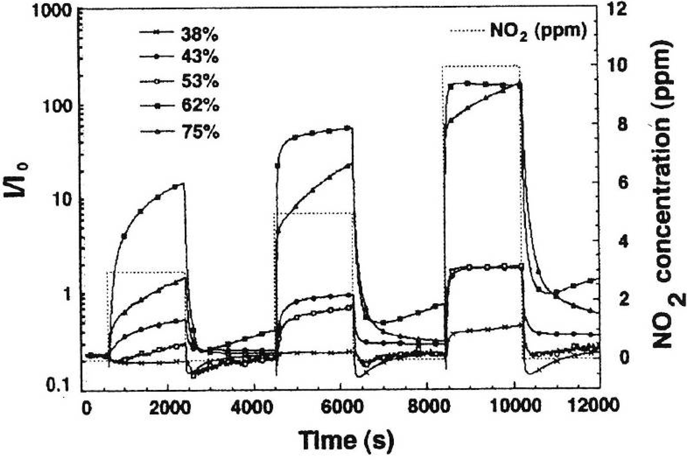
- Boarino, L.; Baratto, C.; Geobaldo, F.; Amato, G.; Comini, E.; Rossi, A.M.; Faglia, G.; Lerondel, G.; Sberveglieri, G. NO2 monitoring at room temperature by a porous silicon gas sensor. Mater. Sci. Eng. B 2000, 69–70, 210–214. [Google Scholar] [CrossRef]
- Pacholski, C.; Sartor, M.; Sailor, M.J.; Cunin, F.; Miskelly, G.M. Biosensing using porous silicon double-layer interferometers: Reflective interferometric Fourier Transform Spectroscopy. J. Am. Chem. Soc. 2005, 127, 11636–11645. [Google Scholar] [CrossRef] [PubMed]
- Sailor, M.J. Sensor applications of porous silicon. In Properties of Porous Silicon; Canham, L., Ed.; INSPEC: London, UK, 1997. [Google Scholar]
- Lauerhaas, J.M.; Credo, G.M.; Heinrich, J.L.; Sailor, M.J. Reversible luminescence quenching of porous silicon by solvents. J. Am. Chem. Soc. 1992, 114, 1911–1912. [Google Scholar] [CrossRef]
- Sancho, A.; Arizti, F.; Gracia, F.J. Porous silicon for the development of capacitive microstructures. Micrelectron. Eng. 2009, 86, 2144–2148. [Google Scholar] [CrossRef]
- Menna, P.; Tsuo, S. Solar cells using porous silicon. In Properties of Porous Silicon; Canham, L., Ed.; INSPEC: London, UK, 1997. [Google Scholar]
- Vitanov, P.; Goranova, E.; Stavrov, V.; Ivanov, P.; Singh, P.K. Fabrication of buried contact in silicon solar cells using porous silicon. Solar Energy Mater. Solar Cell. 2009, 93, 297–300. [Google Scholar] [CrossRef]
- Whitehead, M.A.; Fan, D.; Mukherjee, P.; Akkaraju, G.R.; Canham, L.T.; Coffer, J.L. High-porosity poly(ε-caprolactone)/mesoporous silicon scaffolds: Calcium phosphate deposition and biological response to bone precursor cells. Tissue Eng. A 2008, 14, 195–206. [Google Scholar] [CrossRef]
- Park, J.H.; Gu, L.; Maltzahn, G.; Ruoslahti, E.; Bhatia, S.N.; Sailor, M.J. Biodegradable luminescent porous silicon nanoparticles for in vivo applications. Nat. Mater. 2009, 8, 331–336. [Google Scholar] [CrossRef] [PubMed]
- Lantiat, D.; Toudert, J.; Babonneau, D.; Camelio, S.; Tromas, C.; Simonot, L. Self-organization and optical response of silver nanoparticles dispersed in a dielectric matrix. Rev. Adv. Mater. Sci. 2007, 15, 150–157. [Google Scholar]
- Weissmüller, J.; Newman, R.C.; Jin, H.-J.; Hodge, A.M.; Kysar, J.W. Nanoporous metals by alloy corrosion: Formation and mechanical properties. Mater. Res. Bull. 2009, 34, 577–586. [Google Scholar] [CrossRef]
- Whitney, T.M.; Jiang, J.S.; Searson, P.C.; Chien, C.L. Fabrication of magnetic properties of arrays of metallic nanowires. Science 1993, 261, 1316–1319. [Google Scholar] [CrossRef] [PubMed]
- Kompan, M.E.; Gorodetski, A.E.; Tarasova, I.L. Self formation of porous silicon structure: Primary microscopic mechanism of pore separation. Solid State Phenom. 2004, 97–98, 181–184. [Google Scholar] [CrossRef]
- Helbing, D.; Vicsek, T. Optimal self-organization. New J. Phys. 1999, 1, 13.1–13.7. [Google Scholar] [CrossRef]
- Masuda, H.; Hasegawa, F.; Ono, S. Self-ordering of cell arrangement of anodic porous alumina formed in sulphuric acid solution. J. Electrochem. Soc. 1997, 144, L127–L130. [Google Scholar] [CrossRef]
- Masuda, H.; Fukuda, K. Ordered metal nanohole arrays made by a two-step replication of honeycomb structures of anodic alumina. Science 1995, 268, 1466–1468. [Google Scholar] [CrossRef] [PubMed]
- Zacharatos, F.; Gianneta, V.; Nassiopoulou, A.G. Highly ordered hexagonally arranged sub-200 nm diameter vertical cylindrical pores on p-type Si using non-lithographic pre-patterning of the Si substrate. Phys. Status Solidi A Appl. Res. 2009, 206, 1286–1289. [Google Scholar] [CrossRef]
- Zacharatos, F.; Gianneta, V.; Nassiopoulou, A.G. Highly ordered hexagonally arranged nanostructures on silicon through a self-assembled silicon-integrated porous anodic alumina masking layer. Nanotechnology 2008, 19, 495306. [Google Scholar] [CrossRef] [PubMed]
- Kang, Y.; Jorne, J. Morphological stability analysis of porous silicon formation. J. Electrochem. Soc. 1993, 140, 2258–2265. [Google Scholar] [CrossRef]
- Beale, M.I.J.; Benjamin, J.D.; Uren, M.J.; Chew, N.G.; Cullis, A.G. An experimental and theoretical study of the formation and microstructure of porous silicon. J. Cryst. Growth 1985, 73, 622. [Google Scholar] [CrossRef]
- Zhang, X.G. Morphology and formation mechanisms of porous silicon. J. Electrochem. Soc. 2004, 151, C69–C80. [Google Scholar] [CrossRef]
- Lehmann, V.; Gösele, U. Porous silicon formation: A quantum wire effect. Appl. Phys. Lett. 1991, 58, 856. [Google Scholar] [CrossRef]
- Makushok, Y.E.; Parkhutik, V.P.; Martinez-Duart, J.M.; Albella, J.M. Morphology of passive films formed during electrochemical anodization of materials. J. Phys. D: Appl. Phys. 1994, 27, 661–669. [Google Scholar] [CrossRef]
- Smith, R.L.; Chuang, S.F.; Collins, S.D. A theoretical model of the formation morphologies of porous silicon. J. Electron. Mater. 1988, 17, 533–541. [Google Scholar] [CrossRef]
- John, G.C.; Singh, V.A. Self-organization in porous silicon formation. Phys. Rev. B 1997, 56, 4638–4641. [Google Scholar] [CrossRef]
- Jakubowicz, J.; Szlaferek, A. Computational simulations of pore nucleation in silicon (111). Electrochem. Comm. 2008, 10, 329–334. [Google Scholar]
- Furuta, H.; Matsuda, T.; Yamanaka, C.; Ikeya, M. Self-organized pattern formation in porous silicon using a lattice model with quantum confinement effect. J. Phys. Soc. Jap. 1999, 68, 2218–2220. [Google Scholar] [CrossRef]
- Claussen, J.C.; Carstensen, J.; Christophersen, M.; Langa, S.; Föll, H. Open-loop control of pore formation in semiconductor etching. Proc. Int. Conf. Phys. Control 2003, 3, 895–900. [Google Scholar]
- Emel’yanov, V.I.; Igumnov, V.V.; Starkov, V.V. The dynamics of self-organization of hexagonal pore arrays during anodic etching and oxidation of semiconductors and metals. Tech. Phys. Lett. 2004, 30, 438–440. [Google Scholar] [CrossRef]
- Emel#x2019yanov, V.I.; Eremin, K.I.; Starkov, V.V.; Gavrilin, E.Y. Defect-deformation mechanism of the formation of a pore esemble in semiconductor and metal etching: theory and experiment. Laser Phys. 2003, 13, 1442–1452. [Google Scholar]
- Lehmann, V.; Stengl, R.; Luigart, A. On the morphology and the electrochemical formation mechanism of mesoporous silicon. Mater. Sci. Eng. B 2000, 69–70, 11–22. [Google Scholar] [CrossRef]
- Kompan, M.E. Mechanism of primary self-organization in porous silicon with regular structure. Phys. Solid State 2003, 45, 948–952. [Google Scholar] [CrossRef]
- Ostwald, W. Über die vermeintliche sometrie des roten und gelben Quecksilberoxds und die Oberflächenspannung fester Körper. Z. Phys. Chem. 1900, 34, 495–503. [Google Scholar]
- Lifschitz, I.M.; Sylozov, V.V. The kinetics of precipitation from supersaturated solid solutions. J. Phys. Chem. Solids 1961, 19, 35–50. [Google Scholar] [CrossRef]
- Kleinmann, P.; Badel, X.; Linnros, J. Toward the formation of three-dimensional nanostructures by electrochemical etching of silicon. Appl. Phys. Lett. 2005, 86, 183108. [Google Scholar] [CrossRef]
- Bisi, O.; Ossicini, S.; Pavesi, L. Porous Silicon : a quantum sponge structure for silicon based optoelectronics. Surf. Sci. Rep. 2000, 38, 1–126. [Google Scholar] [CrossRef]
- Rumpf, K.; Granitzer, P.; Pölt, P.; Reichmann, A.; Krenn, H. Self-assembled mesoporous silicon in the crossover between irregular and regular arrangement applicable for Ni filling. Phys. E 2007, 38, 205. [Google Scholar] [CrossRef]
- Rumpf, K.; Granitzer, P.; Pölt, P.; Krenn, H. Transition metals specifically electrodeposited into porous silicon. Phys. Status Solidi C 2009, 6, 1592–1595. [Google Scholar] [CrossRef]
- Rönnebeck, S.; Ottow, S.; Carstensen, J.; Föll, H. Crystal orientation of macropore formation in n-Si with backside-illumination in HF-electrolyte. J. Porous Mater. 2000, 7, 353–356. [Google Scholar] [CrossRef]
- Sze, S.M. Physics of Semiconductor Devices,, 2nd ed.; John Wiley & Sons: Hoboken, NJ, USA, 1981. [Google Scholar]
- Halimaoui, A. Porous silicon: material processing, properties and applications. In Porous Silicon Science and Technology; Vial, J.C., Derrien, J., Eds.; Springer: New York, NY, USA, 1995; Winter School Les Houches, 8–12 February 1994, Les Editions de Physique. [Google Scholar]
- Nakagawa, T.; Sugiyama, H.; Koshida, N. Fabrication of periodic Si nanostructure by controlled anodization. Jpn. J. Appl. Phys. 1998, 37, 7186–7189. [Google Scholar] [CrossRef]
- Hippo, D.; Nakamine, Y.; Urakawa, K.; Tsuchiya, Y.; Mizuta, H.; Koshida, N.; Oda, S. Formation mechanism of 100-nm scale periodic structures in silicon using magnetic-field-assisted anodization. Jpn. J. Appl. Phys. 2008, 47, 7398–7402. [Google Scholar] [CrossRef]
- Gelloz, B.; Masunaga, M.; Shirasawa, T.; Mentek, R.; Ohta, T.; Koshida, N. Enhanced controllability of periodic silicon nanostructures by magnetic field anodization. ECS Trans. 2008, 16, 195–200. [Google Scholar]
- Loni, A.; Canham, L.T.; Berger, M.G.; Arens-Fischer, R.; Münder, H.; Lüth, H.; Arrand, H.F.; Benson, T.M. Porous silicon multilayer optical waveguides. Thin Solid Films 1996, 276, 143–146. [Google Scholar] [CrossRef]
- Wehrspohn, R.B. Linear and non-linear optical experiments based on macroporous silicon photonic crystals. In Nanophotonic Materials, Photonic Crystals, Plasmonics and Metamaterials; Wehrspohn, R.B., Kitzerow, H.-S., Busch, k., Eds.; Wiley-VCH: Weinheim, Germany, 2008. [Google Scholar]
- Perova, T.S.; Tolmachev, V.A.; Astrova, E.V.; Zharova, Yu.A.; O’Neill, S.M. Tunable one-dimensional photonic crystal structures based on grooved Si infiltrated with liquid crystal E7. Phys. Status Solidi C 2007, 4, 1961–1965. [Google Scholar] [CrossRef]
- Granitzer, P.; Rumpf, K.; Pölt, P.; Simic, S.; Krenn, H. Three dimensional quasi regular arrays of Ni nanostructures grown within the pores of a porous silicon layer—magnetic characteristics. Phys. Status Solidi C 2008, 5, 3580. [Google Scholar] [CrossRef]
- Pirota, K.R.; Navas, D.; Hernandez-Velez, M.; Nielsch, K.; Vazquez, M. Novel magnetic materials prepared by electrodeposition techniques: arrays of nanowires and multi-layered microwires. J. Alloys Compd. 2004, 369, 18–26. [Google Scholar] [CrossRef]
- Jeske, M.; Schultze, J.W.; Thönissen, M.; Münder, H. Electrodeposition of metals into porous silicon. Thin Solid Films 1995, 255, 63–66. [Google Scholar] [CrossRef]
- Ronkel, F.; Schultze, J.W.; Arens-Fischer, R. Electrical contact to porous silicon by electrodeposition of iron. Thin Solid Films 1996, 276, 40–43. [Google Scholar] [CrossRef]
- Steiner, P.; Kozlowski, F.; Lang, W. Electroluminescence from porous silicon after metal deposition into the pores. Thin Solid Films 1995, 255, 49–51. [Google Scholar] [CrossRef]
- Jeske, M.; Schultze, J.W.; Münder, H. Porous silicon: Base material for nanotechnologies. Electrochim. Acta 1995, 40, 1435–1438. [Google Scholar] [CrossRef]
- Fang, Ch.; Foca, E.; Xu, S.; Carstensen, J.; Föll, H. Deep silicon macropores filled with Copper by electrodeposition. J. Electrochem. Soc. 2007, 154, D45–D49. [Google Scholar] [CrossRef]
- Fukami, K.; Kobayashi, K.; Matsumoto, T.; Kawamura, Y.L.; Sakka, T.; Ogata, Y.H. Electrodeposition of noble metals into ordered macropores in p-type silicon. J. Electrochem. Soc. 2008, 155, D443–D448. [Google Scholar] [CrossRef]
- Bandarenka, H.; Balucani, M.; Crescenzi, R.; Ferrari, A. Formation of composite nanostructures by corrosive deposition of copper into porous silicon. Superlattices Microstruct. 2008, 44, 583–587. [Google Scholar] [CrossRef]
- Sasano, J.; Jorne, J.; Yoshimi, N.; Tsuboi, T.; Sakka, T.; Ogata, Y.H. Effects of chloride ion on Copper deposition into porous silicon. In Fundamental Aspects of Electrochemical Deposition and Dissolution; Matlosz, M., Landolt, D., Agoaki, R., Sato, Y., Talbot, J.B., Eds.; The Electrochemical Society: Pennington, NJ, USA, 2000. [Google Scholar]
- Fukami, K.; Tanaka, Y.; Chourou, M.L.; Sakka, T.; Ogata, Y.H. Filling of mesoporous silicon with copper by electrodeposition from an aqueous solution. Electrochim. Acta 2009, 54, 2197–2202. [Google Scholar] [CrossRef]
- Ogata, Y.H.; Kobayashi, K.; Motoyama, M. Electrochemical metal deposition on silicon. Curr. Opin. Solid State Mater. Sci. 2006, 10, 163–172. [Google Scholar] [CrossRef]
- Sasano, J.; Schmuki, P.; Sakka, T.; Ogata, Y.H. Laser-assisted nickel deposition onto porous silicon. Phys. Status Solidi A Appl. Res. 2003, 197, 46–50. [Google Scholar] [CrossRef]
- Santinacci, L.; Djenizian, T.; Schwaller, P.; Suter, T.; Etcheberry, A.; Schmuki, P. Selective electrochemical gold deposition onto p-Si (1000) surfaces. J. Phys. D.: Appl. Phys. 2008, 41, 175301. [Google Scholar] [CrossRef]
- Aylett, B.J.; Harding, I.S.; Earwaker, L.G.; Forcey, K.; Giaddui, T. Metallization of porous silicon by chemical vapour infiltration and deposition. Thin Solid Films 1996, 276, 253–256. [Google Scholar] [CrossRef]
- Vazquez, M.; Hernandez-Velez, M.; Pirota, K.; Asenjo, A.; Navas, D.; Velazquez, J.; Vargas, P.; Ramos, C. Arrays of Ni nanowires in alumina membranes: magnetic properties and spatial ordering. Eur. Phys. J. B 2004, 40, 489–497. [Google Scholar] [CrossRef]
- Günther, A.; Monz, S.; Tschöpe, A.; Birringer, R.; Michels, A. Angular dependence and remanence of Ni nanowire arrays and ist relevance to magnetoviscosity. J. Magn. Magn. Mater. 2008, 320, 1340–1344. [Google Scholar] [CrossRef]
- Vazquez, M.; Pirota, K.; Hernandez-Velez, M.; Prida, V.M.; Navas, D.; Sanz, R.; Batallan, F.; Velazquez, J. Magnetic properties of densely packed arrays of Ni nanowires as a function of their diameter and lattice parameter. J. Appl. Phys. 2004, 95, 6642–6644. [Google Scholar] [CrossRef]
- Kumar, A.; Fähler, S.; Schlörb, H.; Leistner, K.; Schultz, L. Competition between shape anisotropy and magnetoelastic anisotropy in Ni nanowires electrodeposited within alumina templates. Phys. Rev. B 2006, 73, 64421. [Google Scholar] [CrossRef]
- Aylett, B.J.; Harding, I.S.; Earwaker, L.G.; Forcey, K.; Giaddui, T. Metallization of porous silicon by chemical vapour infiltration and deposition. Thin Solid Films 1996, 276, 253. [Google Scholar] [CrossRef]
- Granitzer, P.; Rumpf, K.; Pölt, P.; Simic, S.; Krenn, H. Formation of self-assembled metal/silicon nanocomposites. Phys. Status Solidi A Appl. Res. 2008, 205, 1443–1446. [Google Scholar] [CrossRef]
- Xu, C.; Li, M.; Zhang, X.; Tu, K.-N.; Xie, Y. Theoretical studies of displacement deposition of nickel into porous silicon with ultrahigh aspect ratio. Electrochim. Acta 2007, 52, 3901–3009. [Google Scholar] [CrossRef]
- Ramos, C.A.; Vasallo Brigneti, E.; Vazquez, M. Self-organized nanowires: evidence of dipolar interactions from ferromagnetic resonance measurements. Phys. B 2004, 354, 195–197. [Google Scholar] [CrossRef]
- Bicelli, L.P.; Bozzini, B.; Mele, C.; D’Urzo, L. A review of nanostructural aspects of metal electrodeposition. Int. J. Electrochem. Sci. 2008, 3, 356–408. [Google Scholar]
- Julliere, M. Tunneling between ferromagnetic films. Phys. Lett. 1975, 54A, 225–226. [Google Scholar] [CrossRef]
- Jonker, B.T.; Kioseoglou, G.K.; Hanbicki, A.T.; Li, C.H.; Thompson, Ph.E. Electrical spin-injection into silicon from a ferromagnetic metal/tunnel barrier contact. Nat. Phys. 2007, 3, 542–544. [Google Scholar] [CrossRef]
- Granitzer, P.; Rumpf, K.; Pölt, P.; Krenn, H. Porous silicon/metal nanocomposite with tailored magnetic properties. Phys. Status Solidi A Appl. Res. 2009, 206, 1264–1267. [Google Scholar] [CrossRef]
- Stoner, E.C.; Wohlfarth, E.P. A mechanism of magnetic hystereis in heterogeneous alloys. Philos. Trans. R. Soc. London, A 1948, 240, 599–642. [Google Scholar] [CrossRef]
- Granitzer, P.; Rumpf, K.; P#xF6lt, P.; Plank, H.; Albu, M. Ferromagnetic nanostructure arrays self-assembled in mesoporous silicon. J. Phys.: Conf. Ser. 2009, in press. [Google Scholar]
- Granitzer, P.; Rumpf, K.; Poelt, P.; Albu, M.; Chernev, B. The interior interfaces of a semiconductor/metal nanocomposite and their influence on its physical properties. Phys. Status Solidi C 2009, 6, 2222–2227. [Google Scholar] [CrossRef]
- Hyeon, T.; Lee, S.S.; Park, J.; Chang, Y.; Na, H.B. Synthesis of highly crystalline and monodisperse maghemite nanocrystallites without a size-selection process. J. Am. Chem. Soc. 2001, 123, 12798. [Google Scholar] [CrossRef] [PubMed]
- Sun, S.; Zeng, H.J. Size-controlled synthesis of magnetite nanoparticles. Am. Chem. Soc 2002, 124, 8204–8205. [Google Scholar] [CrossRef]
- Yu, W.W.; Falkner, J.C.; Yavuz, C.T.; Colvin, V.L. Synthesis of monodisperse iron oxide nanocrystals by thermal decomposition of iron carboxylate salts. Chem. Commun. 2004, 20, 2306–2307. [Google Scholar] [CrossRef]
- Pileni, M.P.; Feltin, N.; Moumen, N. Nanosized ferrite particles – preparation characterization and magnetic properties. In Scientific and Clinical Applications of Magnetic Carriers; Häfeli, U., Schütt, W., Teller, J., Zborowski, M., Eds.; Plenum Press: New York, NY, USA, 1997. [Google Scholar]
- Canham, L.T. Biomedical applications of porous silicon. In Properties of Porous Silicon; Canham, L.T., Ed.; IEEE Press: London, UK, 1997. [Google Scholar]
- Balakrishnan, S.; Gun’ko, Y.K.; Perova, T.S.; Moore, R.A.; Venkatesan, M.; Douvalis, A.P.; Brouke, P. Dendrite-like self-assembly of magnetite nanoparticles on porous silicon. Small 2006, 2, 864–869. [Google Scholar] [CrossRef] [PubMed]
- Witten, T.A.; Sander, L.M. Diffusion-limited aggregation, a kinetic critical phenomenon. Phys. Rev. Lett. 1981, 47, 1400. [Google Scholar] [CrossRef]
- Granitzer, P.; Rumpf, K.; Roca, A.G.; Morales, M.P.; Pölt, P. Porous silicon /Fe3O4-nanoparticle composite and its magnetic behavior. ECS Trans. 2008, 16, 91–99. [Google Scholar]
- Roca, A.G.; Morales, M.P.; O’Grady, K.; Serna, C.J. Structural and magnetic properties of uniform magnetite nanoparticles prepaed by high temperature decomposition of organic precursors. Nanotechnology 2006, 17, 2783–2788. [Google Scholar] [CrossRef]
- Goya, G.F.; Morales, M.P. Field dependence of blocking temperature in magnetite nanoparticles. J. Metastab. Nanocryst. Mater. 2004, 20–21, 673–678. [Google Scholar] [CrossRef]
- Goya, G.F.; Berquo, T.S.; Fonseca, F.C.; Morales, M. P. Static and dynamic magnetic properties of spherical magnetite nanoparticles. J. Appl. Phys. 2003, 94, 3520–3528. [Google Scholar] [CrossRef]
- Canham, L.T. Bioactive silicon structure fabrication through nanoetching techniques. Adv. Mater. 1995, 7, 1033–1037. [Google Scholar] [CrossRef]
- Coffer, J.L.; Whitehead, M.A.; Nagesha, D.K.; Mukherjee, P.; Akkaraju, G.; Totolici, M.; Saffie, R.S.; Canham, L.T. Porous silicon-based scaffolds for tissue engineering and other biomedical applications. Phys. Status Solidi A Appl. Res. 2005, 202, 1451–1455. [Google Scholar] [CrossRef]
- Thomas, J.Ch.; Pacholski, C.; Sailor, M.J. Delivery of nanogram payload using magnetic porous silicon microcarriers. Royal Soc. Chem. 2006, 6, 782–787. [Google Scholar]
- Park, J.-H.; Derfus, A.M.; Segal, E.; Vecchio, K.S.; Bhatia, S.N.; Sailor, M.J. Local heating of descrete droplets using magnetic porous silicon-based photonic crystals. J. Am. Chem. Soc. 2006, 128, 7938–7946. [Google Scholar] [CrossRef] [PubMed]
© 2010 by the authors; licensee Molecular Diversity Preservation International, Basel, Switzerland. This article is an open-access article distributed under the terms and conditions of the Creative Commons Attribution license (http://creativecommons.org/licenses/by/3.0/).
Share and Cite
Granitzer, P.; Rumpf, K. Porous Silicon—A Versatile Host Material. Materials 2010, 3, 943-998. https://doi.org/10.3390/ma3020943
Granitzer P, Rumpf K. Porous Silicon—A Versatile Host Material. Materials. 2010; 3(2):943-998. https://doi.org/10.3390/ma3020943
Chicago/Turabian StyleGranitzer, Petra, and Klemens Rumpf. 2010. "Porous Silicon—A Versatile Host Material" Materials 3, no. 2: 943-998. https://doi.org/10.3390/ma3020943